SlideShare a Scribd company logo
VLSI routing
   Routing
   Routing Problem
   Routing Regions
   Types of Routing
    -Global Routing
    -Detailed Routing
   Conclusion
   References
o   The routing is to locate a set of wires in the routing space that
    connect all the nets in the net list. The capacities of channels,
    width of wires, and wire crossings often need to be taken into
    consideration .
   Apply after placement
   Input:
      Netlist

      Timing budget for, typically, critical nets

      Locations of blocks and locations of pins

   Output:
      Geometric layouts of all nets

   Objective:
      Minimize the total wire length, the number of vias, or just

       completing all connections without increasing the chip
       area.
      Each net meets its timing budget.
   For a multi-terminal net, we can construct a spanning
    tree to connect all the terminals together.
   But the wire length will be large.
   Better use Steiner Tree:
                                                            Steiner
       A tree connecting all terminals and some              Node
       additional nodes (Steiner nodes).
   Rectilinear Steiner Tree:

       Steiner tree in which all the edges run
       horizontally and vertically.
   Minimum Steiner Tree Problem:
       Given a net, find the steiner tree with the minimum
        length.
       This problem is NP-Complete!
   May need to route tens of thousands of nets simultaneously
    without overlapping.
   Obstacles may exist in the routing region.
Two phases:
Divide the routing area into routing regions of simple shape

(rectangular):                                Switchbox

      Channel


•   Channel: Pins on 2 opposite sides.

•   2-D Switchbox: Pins on 4 sides.

•   3-D Switchbox: Pins on all 6 sides.
VLSI routing
Gate-Array   Standard-Cell   Full-Custom


                  Feedthrough Cell
Routing


                                           Detailed
      Global routing                        routing


                                      Channel         Switch Box
Line Routing     Maze Routing
                                      Routing           Routing
Placement
                                       Global routing

Generate a 'loose' route for each net
Assign a list of routing region to each net
without specifying the actual layout of
wires.

                                        Detailed routing

Find the actual geometry layout of each net
   with in the assigned routing regions


               Compaction
VLSI routing
o   Minimize the total overflow
o   Minimize the total wire length
o   Minimize running time
Assign routing regions to each net. Need to consider timing
budget of nets and routing congestion of the regions.
Assign pins on routing region boundaries for each net.
(Prepare for the detailed routing stage for each region.)
Sequential Approach:
      Route the nets one at a time.
      Order dependent on factors like criticality, estimated wire
       length, etc.
      If further routing is impossible because some nets are
       blocked by nets routed earlier, apply Rip-up and Reroute
       technique.
      This approach is much more popular.
Concurrent Approach:
      The major drawback of the sequential approach is
       that it suffers from the net ordering problem.
      Consider all nets simultaneously.
      Can be formulated as an integer program.
VLSI routing
   Given:
       A planar rectangular grid graph.
       Two points S and T on the graph.
       Obstacles modeled as blocked vertices.
   Objective:
       Find the shortest path connecting S and T.
   This technique can be used in global or detailed routing
    (switchbox) problems.
S              S
                              S 

         T     X             X    
                      T
               X             X       T

Area Routing   Grid Graph     Simplified
                (Maze)      Representation
VLSI routing
VLSI routing
   Three types of detailed routing methods:
    •   Channel Routing
    •   2-D Switchbox Routing
    •   3-D Switchbox Routing
   Channel routing → 2-D switchbox → 3-D switchbox
   If the switchbox or channels are unroutable without a large
    expansion, global routing needs to be done again.
o   Channel routing:
    o   channel may grow in one dimension to accommodate wires;
    o   pins generally on only two opposite sides.
o   Switchbox routing:
    o   Switch box routing is harder than channel routing because we
        can’t expand the switchbox to make room for more wires.
    o   pins are on all four sides, fixing dimensions of the box.
channel   switchbox   switchbox
                      pins


           channel
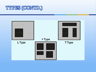
Three types of channel junctions may occur:
o   L-type: Occurs at the corners of the layout surface. Can be
    routed using channel routers.
o   T-type: The leg of the “T” must be routed before the shoulder.
    Can be routed using channel routers.
o   +-type: More complex and requires switchbox routers.
    Advantageous to convert +-junctions to T-junctions.
VLSI routing
   Channel routing is a special case of the routing problem in
    which wires are connected within the routing channels.
   To apply channel routing, a routing region is usually
    decomposed into routing channels.
a)     Channels have no conflicts
b)     Conflicting channels
c)     Conflict resolved using L-shaped channels
     •   Order matters
d)     Switchbox used to resolve the conflict
     •   Order matters
     •   Harder problem (compared to channel routing)
   After global routing and detailed routing, information of the
    nets can be extracted and delays can be analyzed.
   If some nets fail to meet their timing budget, detailed routing
    and/or global routing needs to be repeated.
 NTHU – Route
 MaizeRouter

 BoxRouter

 Archer

 FastRoute

 NTUgr

 FASHION
   Routing is one of the most fundamental steps in the physical
    design flow and is typically a very complex optimization
    problem.
   Effective and efficient routing algorithms are essential to handle
    the challenges arising from the fast growing scaling of IC
    integration.
   We have discussed Global and Detailed routing techniques.
   Routers will keep evolving with emerging design challenges such
    as nanometer effects, signal integrity, reliability etc.
                      33
   “Global and detailed routing”, Huang-Yu Chen and Yao-Wen Chang,
    National Taiwan University, Taipei, Taiwan,
   “VLSI Layout synthesis”, Local search in Combinatorial Optimization,
    Emile H.L. Aarts, Philips Research Laboratories, Eindhoven.
   Michael D. Moffitt, IBM Research “Global routing revisited”. Computer-
    Aided Design - Digest of Technical Papers, 2009. ICCAD 2009.
    IEEE/ACM International Conference , Pages: 805 - 808
35

More Related Content

What's hot (20)

PDF
VLSI-Physical Design- Tool Terminalogy
Murali Rai
 
PPTX
Vlsi physical design
I World Tech
 
PPTX
Multi mode multi corner (mmmc)
shaik sharief
 
PPTX
Powerplanning
VLSI SYSTEM Design
 
PPTX
Pass Transistor Logic
Sudhanshu Janwadkar
 
PPTX
Vlsi stick daigram (JCE)
Hrishikesh Kamat
 
PPTX
Flip Chip technology
Mantra VLSI
 
PPTX
Study of vlsi design methodologies and limitations using cad tools for cmos t...
Lakshmi Narain College of Technology & Science Bhopal
 
PDF
Chapter1.slides
Avinash Pillai
 
PDF
Physical design-complete
Murali Rai
 
PDF
Sta by usha_mehta
Usha Mehta
 
PPTX
System partitioning in VLSI and its considerations
Subash John
 
PDF
Digital VLSI Design : Introduction
Usha Mehta
 
PDF
Design for Testability
kumar gavanurmath
 
PPTX
Vlsi design flow
Rajendra Kumar
 
PPTX
Layout & Stick Diagram Design Rules
varun kumar
 
PPT
Timing and Design Closure in Physical Design Flows
Olivier Coudert
 
PDF
VLSI Fresher Resume
vikas kumar
 
PPTX
Vlsi physical design automation on partitioning
Sushil Kundu
 
PPTX
MOS transistor 13
HIMANSHU DIWAKAR
 
VLSI-Physical Design- Tool Terminalogy
Murali Rai
 
Vlsi physical design
I World Tech
 
Multi mode multi corner (mmmc)
shaik sharief
 
Powerplanning
VLSI SYSTEM Design
 
Pass Transistor Logic
Sudhanshu Janwadkar
 
Vlsi stick daigram (JCE)
Hrishikesh Kamat
 
Flip Chip technology
Mantra VLSI
 
Study of vlsi design methodologies and limitations using cad tools for cmos t...
Lakshmi Narain College of Technology & Science Bhopal
 
Chapter1.slides
Avinash Pillai
 
Physical design-complete
Murali Rai
 
Sta by usha_mehta
Usha Mehta
 
System partitioning in VLSI and its considerations
Subash John
 
Digital VLSI Design : Introduction
Usha Mehta
 
Design for Testability
kumar gavanurmath
 
Vlsi design flow
Rajendra Kumar
 
Layout & Stick Diagram Design Rules
varun kumar
 
Timing and Design Closure in Physical Design Flows
Olivier Coudert
 
VLSI Fresher Resume
vikas kumar
 
Vlsi physical design automation on partitioning
Sushil Kundu
 
MOS transistor 13
HIMANSHU DIWAKAR
 

Similar to VLSI routing (20)

PPT
Routing.ppt
Sunesh N.V
 
PDF
MODULE2-Routing ADVANVECD VLSI VTU2024.pdf
narayanakiran2
 
PDF
COMPUTER NETWORKS CHAPTER 3 NETWORK LAYER NOTES CSE 3RD year sem 1
aishwaryaarrao3
 
PPTX
21EC71_Module-2_Routing PPT Electronics and communication engineering module 2
yashithkumarbr
 
PPTX
Physical organization of parallel platforms
Syed Zaid Irshad
 
PDF
minimisation of crosstalk in VLSI routing
Chandrajit Pal
 
PPT
Channel routing
sanjay bahuguna
 
PPTX
floorplanning in advanced vlsi module off 1
BalajiShankar12
 
PPT
Lecture24 clockpower routing
freeloadtailieu
 
PPT
Network layer
TharuniDiddekunta
 
PDF
Module 2 Floor Planning and Placement.pdf
ShyamalaC7
 
PPT
Network
Daksh Bapna
 
PPT
L22.ppt
raaed5
 
PDF
Synchronous optical networking (SONET)
Jyothishmathi Institute of Technology and Science Karimnagar
 
PPT
24-ad-hoc.ppt
sumadi26
 
PPTX
Routing Presentation
Mohsin Ali
 
PDF
Taiwan course
Bharath Kumar
 
PDF
Radio Resource Management for Millimeter Wave & Massive MIMO
Eduardo Castañeda
 
PPT
Parallel computing chapter 2
Md. Mahedi Mahfuj
 
PPT
system interconnect architectures in ACA
Pankaj Kumar Jain
 
Routing.ppt
Sunesh N.V
 
MODULE2-Routing ADVANVECD VLSI VTU2024.pdf
narayanakiran2
 
COMPUTER NETWORKS CHAPTER 3 NETWORK LAYER NOTES CSE 3RD year sem 1
aishwaryaarrao3
 
21EC71_Module-2_Routing PPT Electronics and communication engineering module 2
yashithkumarbr
 
Physical organization of parallel platforms
Syed Zaid Irshad
 
minimisation of crosstalk in VLSI routing
Chandrajit Pal
 
Channel routing
sanjay bahuguna
 
floorplanning in advanced vlsi module off 1
BalajiShankar12
 
Lecture24 clockpower routing
freeloadtailieu
 
Network layer
TharuniDiddekunta
 
Module 2 Floor Planning and Placement.pdf
ShyamalaC7
 
Network
Daksh Bapna
 
L22.ppt
raaed5
 
Synchronous optical networking (SONET)
Jyothishmathi Institute of Technology and Science Karimnagar
 
24-ad-hoc.ppt
sumadi26
 
Routing Presentation
Mohsin Ali
 
Taiwan course
Bharath Kumar
 
Radio Resource Management for Millimeter Wave & Massive MIMO
Eduardo Castañeda
 
Parallel computing chapter 2
Md. Mahedi Mahfuj
 
system interconnect architectures in ACA
Pankaj Kumar Jain
 
Ad

More from Naveen Kumar (20)

PPT
Security in GSM(2G) and UMTS(3G) Networks
Naveen Kumar
 
PPTX
Mobile tower radiation
Naveen Kumar
 
PPTX
Mobile security
Naveen Kumar
 
PPTX
Ph.D Research proposal
Naveen Kumar
 
PPTX
Wi-Fi Technology
Naveen Kumar
 
PPTX
Cell Phone Antennas
Naveen Kumar
 
PPT
Thesis on PIFA
Naveen Kumar
 
PPTX
Electronics Quiz
Naveen Kumar
 
DOC
VHDL coding in Xilinx
Naveen Kumar
 
DOC
Optimization in HFSS
Naveen Kumar
 
PPT
Free space optical communication
Naveen Kumar
 
PDF
A Multi-Band PIFA with Slotted Ground Plane
Naveen Kumar
 
PDF
Study of Planar Inverted - F Antenna (PIFA) for mobile devices
Naveen Kumar
 
PDF
A novel low profile planar inverted f antenna (pifa) for mobile handsets
Naveen Kumar
 
PDF
A compact planar inverted-F antenna with slotted ground plane
Naveen Kumar
 
PPT
Secure Socket Layer
Naveen Kumar
 
PPT
Adaptive Resonance Theory
Naveen Kumar
 
PPT
UART
Naveen Kumar
 
PPT
HDLC, PPP and SLIP
Naveen Kumar
 
PPT
AR model
Naveen Kumar
 
Security in GSM(2G) and UMTS(3G) Networks
Naveen Kumar
 
Mobile tower radiation
Naveen Kumar
 
Mobile security
Naveen Kumar
 
Ph.D Research proposal
Naveen Kumar
 
Wi-Fi Technology
Naveen Kumar
 
Cell Phone Antennas
Naveen Kumar
 
Thesis on PIFA
Naveen Kumar
 
Electronics Quiz
Naveen Kumar
 
VHDL coding in Xilinx
Naveen Kumar
 
Optimization in HFSS
Naveen Kumar
 
Free space optical communication
Naveen Kumar
 
A Multi-Band PIFA with Slotted Ground Plane
Naveen Kumar
 
Study of Planar Inverted - F Antenna (PIFA) for mobile devices
Naveen Kumar
 
A novel low profile planar inverted f antenna (pifa) for mobile handsets
Naveen Kumar
 
A compact planar inverted-F antenna with slotted ground plane
Naveen Kumar
 
Secure Socket Layer
Naveen Kumar
 
Adaptive Resonance Theory
Naveen Kumar
 
HDLC, PPP and SLIP
Naveen Kumar
 
AR model
Naveen Kumar
 
Ad

Recently uploaded (20)

PPTX
Digital Circuits, important subject in CS
contactparinay1
 
PPT
Ericsson LTE presentation SEMINAR 2010.ppt
npat3
 
PPTX
Mastering ODC + Okta Configuration - Chennai OSUG
HathiMaryA
 
PDF
AI Agents in the Cloud: The Rise of Agentic Cloud Architecture
Lilly Gracia
 
PDF
UiPath DevConnect 2025: Agentic Automation Community User Group Meeting
DianaGray10
 
PPTX
Future Tech Innovations 2025 – A TechLists Insight
TechLists
 
PPTX
COMPARISON OF RASTER ANALYSIS TOOLS OF QGIS AND ARCGIS
Sharanya Sarkar
 
PPTX
New ThousandEyes Product Innovations: Cisco Live June 2025
ThousandEyes
 
PDF
Mastering Financial Management in Direct Selling
Epixel MLM Software
 
PDF
NLJUG Speaker academy 2025 - first session
Bert Jan Schrijver
 
PPTX
From Sci-Fi to Reality: Exploring AI Evolution
Svetlana Meissner
 
PPTX
Seamless Tech Experiences Showcasing Cross-Platform App Design.pptx
presentifyai
 
PPTX
The Project Compass - GDG on Campus MSIT
dscmsitkol
 
PDF
Peak of Data & AI Encore AI-Enhanced Workflows for the Real World
Safe Software
 
PPTX
Q2 FY26 Tableau User Group Leader Quarterly Call
lward7
 
PDF
SIZING YOUR AIR CONDITIONER---A PRACTICAL GUIDE.pdf
Muhammad Rizwan Akram
 
PDF
The 2025 InfraRed Report - Redpoint Ventures
Razin Mustafiz
 
PPTX
Designing_the_Future_AI_Driven_Product_Experiences_Across_Devices.pptx
presentifyai
 
PDF
CIFDAQ Market Wrap for the week of 4th July 2025
CIFDAQ
 
PPTX
AI Penetration Testing Essentials: A Cybersecurity Guide for 2025
defencerabbit Team
 
Digital Circuits, important subject in CS
contactparinay1
 
Ericsson LTE presentation SEMINAR 2010.ppt
npat3
 
Mastering ODC + Okta Configuration - Chennai OSUG
HathiMaryA
 
AI Agents in the Cloud: The Rise of Agentic Cloud Architecture
Lilly Gracia
 
UiPath DevConnect 2025: Agentic Automation Community User Group Meeting
DianaGray10
 
Future Tech Innovations 2025 – A TechLists Insight
TechLists
 
COMPARISON OF RASTER ANALYSIS TOOLS OF QGIS AND ARCGIS
Sharanya Sarkar
 
New ThousandEyes Product Innovations: Cisco Live June 2025
ThousandEyes
 
Mastering Financial Management in Direct Selling
Epixel MLM Software
 
NLJUG Speaker academy 2025 - first session
Bert Jan Schrijver
 
From Sci-Fi to Reality: Exploring AI Evolution
Svetlana Meissner
 
Seamless Tech Experiences Showcasing Cross-Platform App Design.pptx
presentifyai
 
The Project Compass - GDG on Campus MSIT
dscmsitkol
 
Peak of Data & AI Encore AI-Enhanced Workflows for the Real World
Safe Software
 
Q2 FY26 Tableau User Group Leader Quarterly Call
lward7
 
SIZING YOUR AIR CONDITIONER---A PRACTICAL GUIDE.pdf
Muhammad Rizwan Akram
 
The 2025 InfraRed Report - Redpoint Ventures
Razin Mustafiz
 
Designing_the_Future_AI_Driven_Product_Experiences_Across_Devices.pptx
presentifyai
 
CIFDAQ Market Wrap for the week of 4th July 2025
CIFDAQ
 
AI Penetration Testing Essentials: A Cybersecurity Guide for 2025
defencerabbit Team
 

VLSI routing

  • 2. Routing  Routing Problem  Routing Regions  Types of Routing -Global Routing -Detailed Routing  Conclusion  References
  • 3. o The routing is to locate a set of wires in the routing space that connect all the nets in the net list. The capacities of channels, width of wires, and wire crossings often need to be taken into consideration .
  • 4. Apply after placement  Input:  Netlist  Timing budget for, typically, critical nets  Locations of blocks and locations of pins  Output:  Geometric layouts of all nets  Objective:  Minimize the total wire length, the number of vias, or just completing all connections without increasing the chip area.  Each net meets its timing budget.
  • 5. For a multi-terminal net, we can construct a spanning tree to connect all the terminals together.  But the wire length will be large.  Better use Steiner Tree: Steiner A tree connecting all terminals and some Node additional nodes (Steiner nodes).  Rectilinear Steiner Tree: Steiner tree in which all the edges run horizontally and vertically.
  • 6. Minimum Steiner Tree Problem:  Given a net, find the steiner tree with the minimum length.  This problem is NP-Complete!  May need to route tens of thousands of nets simultaneously without overlapping.  Obstacles may exist in the routing region.
  • 8. Divide the routing area into routing regions of simple shape (rectangular): Switchbox Channel • Channel: Pins on 2 opposite sides. • 2-D Switchbox: Pins on 4 sides. • 3-D Switchbox: Pins on all 6 sides.
  • 10. Gate-Array Standard-Cell Full-Custom Feedthrough Cell
  • 11. Routing Detailed Global routing routing Channel Switch Box Line Routing Maze Routing Routing Routing
  • 12. Placement Global routing Generate a 'loose' route for each net Assign a list of routing region to each net without specifying the actual layout of wires. Detailed routing Find the actual geometry layout of each net with in the assigned routing regions Compaction
  • 14. o Minimize the total overflow o Minimize the total wire length o Minimize running time
  • 15. Assign routing regions to each net. Need to consider timing budget of nets and routing congestion of the regions.
  • 16. Assign pins on routing region boundaries for each net. (Prepare for the detailed routing stage for each region.)
  • 17. Sequential Approach:  Route the nets one at a time.  Order dependent on factors like criticality, estimated wire length, etc.  If further routing is impossible because some nets are blocked by nets routed earlier, apply Rip-up and Reroute technique.  This approach is much more popular.
  • 18. Concurrent Approach:  The major drawback of the sequential approach is that it suffers from the net ordering problem.  Consider all nets simultaneously.  Can be formulated as an integer program.
  • 20. Given:  A planar rectangular grid graph.  Two points S and T on the graph.  Obstacles modeled as blocked vertices.  Objective:  Find the shortest path connecting S and T.  This technique can be used in global or detailed routing (switchbox) problems.
  • 21. S S S  T X X  T X X  T Area Routing Grid Graph Simplified (Maze) Representation
  • 24. Three types of detailed routing methods: • Channel Routing • 2-D Switchbox Routing • 3-D Switchbox Routing  Channel routing → 2-D switchbox → 3-D switchbox  If the switchbox or channels are unroutable without a large expansion, global routing needs to be done again.
  • 25. o Channel routing: o channel may grow in one dimension to accommodate wires; o pins generally on only two opposite sides. o Switchbox routing: o Switch box routing is harder than channel routing because we can’t expand the switchbox to make room for more wires. o pins are on all four sides, fixing dimensions of the box.
  • 26. channel switchbox switchbox pins channel
  • 27. Three types of channel junctions may occur: o L-type: Occurs at the corners of the layout surface. Can be routed using channel routers. o T-type: The leg of the “T” must be routed before the shoulder. Can be routed using channel routers. o +-type: More complex and requires switchbox routers. Advantageous to convert +-junctions to T-junctions.
  • 29. Channel routing is a special case of the routing problem in which wires are connected within the routing channels.  To apply channel routing, a routing region is usually decomposed into routing channels.
  • 30. a) Channels have no conflicts b) Conflicting channels c) Conflict resolved using L-shaped channels • Order matters d) Switchbox used to resolve the conflict • Order matters • Harder problem (compared to channel routing)
  • 31. After global routing and detailed routing, information of the nets can be extracted and delays can be analyzed.  If some nets fail to meet their timing budget, detailed routing and/or global routing needs to be repeated.
  • 32.  NTHU – Route  MaizeRouter  BoxRouter  Archer  FastRoute  NTUgr  FASHION
  • 33. Routing is one of the most fundamental steps in the physical design flow and is typically a very complex optimization problem.  Effective and efficient routing algorithms are essential to handle the challenges arising from the fast growing scaling of IC integration.  We have discussed Global and Detailed routing techniques.  Routers will keep evolving with emerging design challenges such as nanometer effects, signal integrity, reliability etc. 33
  • 34. “Global and detailed routing”, Huang-Yu Chen and Yao-Wen Chang, National Taiwan University, Taipei, Taiwan,  “VLSI Layout synthesis”, Local search in Combinatorial Optimization, Emile H.L. Aarts, Philips Research Laboratories, Eindhoven.  Michael D. Moffitt, IBM Research “Global routing revisited”. Computer- Aided Design - Digest of Technical Papers, 2009. ICCAD 2009. IEEE/ACM International Conference , Pages: 805 - 808
  • 35. 35