DSD
7 likes2,667 views

This document discusses various digital system implementation options including ROM, PROM, EPROM, EEPROM, sequential circuits using ROMs, PLDs, ASICs and FPGAs. It describes the basic structure and characteristics of ROMs, PROMs, PLDs like PLA, PAL, CPLDs and different types of ASICs including full-custom, standard-cell based, gate-array based and structured gate arrays. It also provides examples of implementing functions using PAL and discusses the core structure of FPGAs.


DSD
- 1. Digital System Implementation Options Dr. D. V. Kamath Professor, Department of E&C Engg., Manipal Institute of Technology, Manipal 1
- 2. 2 ROM All types of ROMs are non-volatile i.e., Data is retained when power is removed Generally not in-system writeable
- 3. 3 Types of ROMs ROM : Read Only Memory PROM : Programmable ROM EPROM : Erasable Programmable ROM EEPROM : Electrically Erasable Programmable ROM EAROM : Electrically Alterable ROM
- 4. 4 ROM and PROM ROMs and PROMs Not erasable Used for storing high volume data ROM Mask programmed by the manufacturer PROM Programmed by the user
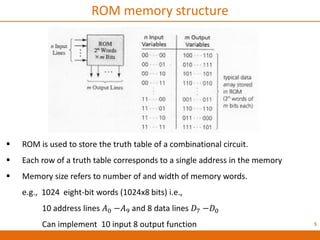
- 5. 5 ROM memory structure ROM is used to store the truth table of a combinational circuit. Each row of a truth table corresponds to a single address in the memory Memory size refers to number of and width of memory words. e.g., 1024 eight-bit words (1024x8 bits) i.e., 10 address lines 𝐴0 −𝐴9 and 8 data lines 𝐷7 −𝐷0 Can implement 10 input 8 output function
- 6. 6 ROM memory structure The memory structure includes array of memory cells and address decoder The memory structure includes array of memory cells and address decoder
- 7. 7 Combinational circuit implementation using ROMs
- 8. 8 The sequential circuits can be implemented using ROM by storing the state table The present state and present input are applied on address lines. The data outputs consist of next state and present output Both Mealy and Moore machines can be realized. (The output of Moore machine lags by one clock period) Sequential circuit implementation using ROMs
- 9. 9 Digital circuit implementation choices Custom Standard Cells Macro Cells Cell-based Pre-diffused (Gate Arrays) Pre-wired (FPGAs) Array-based Semicustom Digital Circuit Implementation Approaches
- 10. 10 PLD as a black box Input Variables . . . . . . Logic Gates And Switches Output Values (function values) Programmable Logic Device (PLD) is a chip that is manufactured with a programmable configuration, enabling it to serve in many arbitrary applications
- 11. 11 PLD structure All different types of PLDs have an AND-OR structure
- 12. 12 Types of PLDs Depending on the type of AND-OR planes, PLDs are classified as follows: Programmable read-only memory (PROM) Programmable logic array (PLA) Programmable array logic (PAL) PLD AND Plane OR Plane PROM Fixed Programmable PLA Programmable Programmable PAL Programmable Fixed
- 13. 13 PLD notation Notation for Programmable AND gate
- 14. 14 PLD notation Notation for Programmable OR gate
- 15. 15 PLD notation Special notation for Programmable AND/ OR gate with no fuses blown
- 16. 16 PLD notation
- 18. 18 Generic PLA structure 𝑿 𝒏 . . . Input (buffers & inverters) . . . . . . AND plane … OR plane 𝒁 𝒎 Programmable Logic Array (PLA) structures provide a logical and compact method of implementation of multiple SOP(Sum of Products) or POS(Product of Sums) expressions Suited for implementation of two-level combinational logic To implement the sequential logic, additional memory element i.e., Flip-Flops are needed
- 19. 19 PLA Typical AND-OR floor plan used in PLA implementation
- 20. 20 PLA structures NMOS PLA is usually implemented using NOR-NOR plane
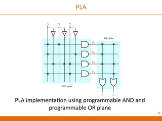
- 21. 21 PLA PLA implementation using programmable AND and programmable OR plane
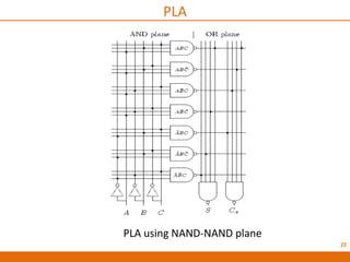
- 22. 22 PLA PLA using NAND-NAND plane
- 23. 23 Programmable Array Logic(PAL) PAL A programmable AND array and a fixed OR array Merits: Easier to program Demerits: Not as flexible as PLA
- 24. 24 Programmable Array Logic(PAL) Typical PAL architecture with fixed sequential circuit in the form of D-type flip- flop macro cell
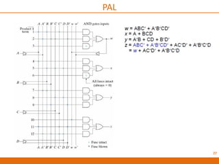
- 25. 25 PAL Typical PAL with 4 inputs , 4 outputs, and 3-wide AND-OR structure PAL consists of 4 sections of 3-wide AND-OR array
- 26. 26 PAL Implement the following functions using PAL 𝑊 𝐴, 𝐵, 𝐶, 𝐷 = ∑ (2, 12, 13) 𝑋 𝐴, 𝐵, 𝐶, 𝐷 = ∑(7, 8, 9, 10, 11, 12, 13, 14, 15) 𝑌 𝐴, 𝐵, 𝐶, 𝐷 = ∑(0,2, 3,4, 5,6,7,8,10,11,15) 𝑍 𝐴, 𝐵, 𝐶, 𝐷 = ∑(1,2,8,12,13)
- 27. 27 PAL
- 28. 28 TYPES OF ASICS Full-Custom ASICs Standard-Cell–Based ASICs Gate-Array–Based ASICs Channeled Gate Array Channelless Gate Array Structured Gate Array Programmable Logic Devices/ Complex PLDs(CPLDs) Field-Programmable Gate Arrays
- 29. 29 ASIC ASIC - Application Specific Integrated Circuit In Integrated Circuit (IC) designed to perform a specific function for a specific application As opposed to a standard, general purpose off-the-shelf part such as a commercial microprocessor IC Levels of integration: SSI - Small scale integration MSI - Medium scale integration LSI - Large scale integration VLSI - Very large scale integration USLI - Ultra large scale integration Implementation technology TTL ECL MOS - NMOS, CMOS
- 30. 30 Full-Custom ASIC All mask layers are customized in a full-custom ASIC Generally, the designer lays out all cells by hand Some automatic placement and routing may be done Critical (timing) paths are usually laid out completely by hand Full-custom design offers the highest performance and smallest die size for a given design The disadvantages of full-custom design include increased design time, complexity, design expense, and highest risk Microprocessors were exclusively full-custom, but designers are increasingly turning to semicustom ASIC techniques in this area as well Other application examples of full-custom ICs or ASICs are requirements in automobile, analog/digital communications, military applications.
- 32. 32 Standard-Cell-Based ASICs A cell-based ASIC ( CBIC-“sea-bick”) Standard cells Possibly megacells , megafunctions , full-custom blocks , system-level macros( SLMs ), fixed blocks , cores , or Functional Standard Blocks ( FSBs ) All mask layers are customized - transistors and interconnect Automated buffer sizing, placement and routing Custom blocks can be embedded
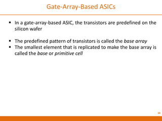
- 34. 34 Gate-Array-Based ASICs In a gate-array-based ASIC, the transistors are predefined on the silicon wafer The predefined pattern of transistors is called the base array The smallest element that is replicated to make the base array is called the base or primitive cell
- 35. 35 Masked Gate Array (MGA) ASICs Masked Gate Array (MGA)/Mask Programmable Gate Array (MPGA) The top level interconnect between the transistors is defined by the designer in custom masks Design is performed by connecting predesigned and characterized logic cells from a library (macros) After validation, automatic placement and routing are typically used to convert the macro-based design into a layout on the ASIC using primitive cells Types of MGAs: Channeled Gate Array Channelless Gate Array Structured Gate Array
- 36. 36 Channeled Gate Array Channeled Gate Array Only the interconnect is customized The interconnect uses predefined spaces between rows of base cells Wafers containing arrays of cells Interconnections Actual Design
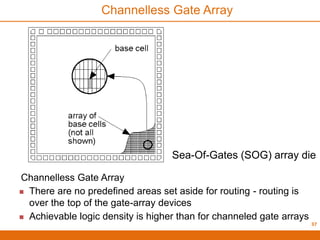
- 37. 37 Channelless Gate Array Sea-Of-Gates (SOG) array die Channelless Gate Array There are no predefined areas set aside for routing - routing is over the top of the gate-array devices Achievable logic density is higher than for channeled gate arrays
- 38. 38 Structured Gate Array Structured Gate Array Only the interconnect is customized Custom blocks can be embedded • These can be complete blocks such as a processor or memory array, or • an array of different base cells better suited to implementing a specific function
- 39. 39 CPLD structure CPLD die Complex Programmable Logic Devices (CPLDs) No customized mask layers or logic cells Fast design turnaround A single large block of programmable interconnect Erasable PLD (EPLD) Mask-programmed PLD A matrix of logic macro cells that usually consist of Programmable Array Logic(PAL) followed by a flip-flop or latch
- 40. 40 FPGA structure FPGA die Field Programmable Gate Array None of the mask layers are customized A method for programming the basic logic cells and the interconnect The core is a regular array of programmable basic logic cells that can implement combinational as well as sequential logic (flip-flops) A matrix of programmable interconnect surrounds the basic logic cells Programmable I/O cells surround the core