
![COURSE CONTENTS:
Unit I: Introduction to VLSI Design: Introduction to VLSI Design; Moore’s Law; Scale of
Integration; Types of VLSI Chips; Design principles (Digital VLSI); Design Domains(Y-Chart),
Challenges of VLSI design- power, timing area, noise, testability reliability, and yield; CAD tools for
VLSI design. [6L]
Unit II: VLSI Circuit Design Processes: Basic CMOS Technology, n-well CMOS process, p-well
CMOS VLSI Design process, Twin tub process, Silicon on insulator; CMOS process enhancement-
Interconnect; circuit elements, Stick Diagrams, Design Rules and Layouts, Lambda based design
rules, Contact cuts, CMOS Lambda and Micron based design rules, Layout Diagrams for logic gates,
Transistor structures, wires and vias, Scaling of MOS circuits- Scaling models, scaling factors, scaling
factors for device parameters, Limitations of Scaling. [8L]
Unit III: Analysis of CMOS logic Circuits: MOSFET as Switch; Recapitulation of MOS; CMOS
Inverter, Noise Margin, CMOS logic circuits; NAND gate and NOR Gate; Complex logic circuits;
Pass transistor logic; CMOS Transmission gate; CMOS full adder. [10L]
Unit IV: Advanced Techniques in CMOS logic circuit: Pseudo nMOS; Tri-state; Clocked CMOS;
Dynamic CMOS logic- Domino, NORA, Zipper, etc.; Dual rail logic networks. [8L]
Unit V: Memories: Static RAM; SRAM arrays; Dynamic RAMs; ROM arrays; Logic arrays, FPGAs,
CPLDs. [5L]
Unit VI: Testing and Testability: Motivation for testing, Design for testability, the problems of digital
and analog testing, Design for test, Faults in Digital Circuits: Controllability, and Observability, Fault
models – stuck-at faults, Bridging Fault, Testing Techniques.](https://image.slidesharecdn.com/vlsiunit1technology-s-230505172751-11eb6469/85/VLSI-unit-1-Technology-S-ppt-2-320.jpg)


VLSI unit 1 Technology - S.ppt
- 1. VLSI Design Dr Pushpa Giri Asst. Prof., ECE dept.
- 2. COURSE CONTENTS: Unit I: Introduction to VLSI Design: Introduction to VLSI Design; Moore’s Law; Scale of Integration; Types of VLSI Chips; Design principles (Digital VLSI); Design Domains(Y-Chart), Challenges of VLSI design- power, timing area, noise, testability reliability, and yield; CAD tools for VLSI design. [6L] Unit II: VLSI Circuit Design Processes: Basic CMOS Technology, n-well CMOS process, p-well CMOS VLSI Design process, Twin tub process, Silicon on insulator; CMOS process enhancement- Interconnect; circuit elements, Stick Diagrams, Design Rules and Layouts, Lambda based design rules, Contact cuts, CMOS Lambda and Micron based design rules, Layout Diagrams for logic gates, Transistor structures, wires and vias, Scaling of MOS circuits- Scaling models, scaling factors, scaling factors for device parameters, Limitations of Scaling. [8L] Unit III: Analysis of CMOS logic Circuits: MOSFET as Switch; Recapitulation of MOS; CMOS Inverter, Noise Margin, CMOS logic circuits; NAND gate and NOR Gate; Complex logic circuits; Pass transistor logic; CMOS Transmission gate; CMOS full adder. [10L] Unit IV: Advanced Techniques in CMOS logic circuit: Pseudo nMOS; Tri-state; Clocked CMOS; Dynamic CMOS logic- Domino, NORA, Zipper, etc.; Dual rail logic networks. [8L] Unit V: Memories: Static RAM; SRAM arrays; Dynamic RAMs; ROM arrays; Logic arrays, FPGAs, CPLDs. [5L] Unit VI: Testing and Testability: Motivation for testing, Design for testability, the problems of digital and analog testing, Design for test, Faults in Digital Circuits: Controllability, and Observability, Fault models – stuck-at faults, Bridging Fault, Testing Techniques.
- 3. VLSI – Very Large Scale Integration This is the field which involves packing more and more logic devices into smaller and smaller areas. — VLSI circuits are everywhere … your computer, your car, your brand new state-of-the-art digital camera, the cell- phones… Refers to the many fields of electrical and computer engineering that deal with the analysis and design of very dense electronic integrated circuits
- 4. Design Hierarchy System Specifications Abstract high-level model Logic Synthesis Circuit Design Physical Design Manufacturing Finished VLSI Chip
- 5. VLSI:Very Large Scale Integration Integration: Integrated Circuits multiple devices on one substrate How large is Very Large? SSI (small scale integration) 7400 series, 10-100 transistors MSI (medium scale) 74000 series 100-1000 LSI 1,000-10,000 transistors VLSI > 20,000 transistors ULSI/SLSI (some disagreement)
- 6. Integration Reduces Manufacturing Costs • (almost) no manual assembly • About $1-5billion/fab • Typical Fab 1 city block, a few hundred people • Packaging is largest cost • Testing is second largest cost • For low volume ICs, Design Cost may swamp all manufacturing cost WHY VLSI? Integration improves the design. Following are the design metrics can be achieved by VLSI design: — Higher speed — Lower power — Physically smaller — Integration reduces manufacturing cost — Higher reliability — More functionality
- 7. VLSI Chip Types Full-custom Every circuit is designed for the project Application-specific integrated circuits (ASIC) Allow designers to create IC’s for a particular application Semi-custom Between full-custom and ASIC
- 8. VLSI Chip Types Full-custom Time, Cost Application-specific integrated circuits (ASIC) Allow designers to create IC’s for a particular application Semi-custom Less opportunity for performance improvement
- 10. A Brief History Invention of the Transistor Vacuum tubes ruled in first half of 20th century Large, expensive, power-hungry, unreliable 1947: first point contact transistor (3 terminal devices) Shockley, Bardeen and Brattain at Bell Labs
- 11. A Brief History, contd.. 1958: First integrated circuit Flip-flop using two transistors Built by Jack Kilby (Nobel Laureate) at Texas Instruments Robert Noyce (Fairchild) is also considered as a co-inventor
- 12. A Brief History, contd. First Planer IC built in 1961 2003 Intel Pentium 4 processor (55 million transistors) 512 Mbit DRAM (> 0.5 billion transistors) 53% compound annual growth rate over 45 years No other technology has grown so fast so long Driven by miniaturization of transistors Smaller is cheaper, faster, lower in power! Revolutionary effects on society RCA 16-transistor MOSFET IC
- 13. 1970’s processes usually had only nMOS transistors Inexpensive, but consume power while idle 1980s-present: CMOS processes for low idle power MOS Integrated Circuits Intel 1101 256-bit SRAM Intel 4004 4-bit Proc
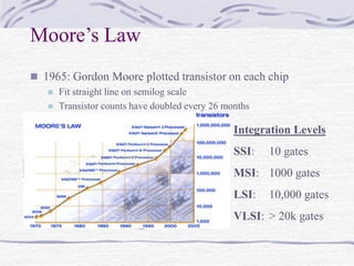
- 14. Moore’s Law 1965: Gordon Moore plotted transistor on each chip Fit straight line on semilog scale Transistor counts have doubled every 26 months Year Transistors 4004 8008 8080 8086 80286 Intel386 Intel486 Pentium Pentium Pro Pentium II Pentium III Pentium 4 1,000 10,000 100,000 1,000,000 10,000,000 100,000,000 1,000,000,000 1970 1975 1980 1985 1990 1995 2000 Integration Levels SSI: 10 gates MSI: 1000 gates LSI: 10,000 gates VLSI: > 20k gates
- 15. Example: Intel Processor Sizes Intel386TM DX Processor Intel486TM DX Processor Pentium® Processor Pentium® Pro & Pentium® II Processors 1.5 1.0 0.8 0.6 0.35 0.25 Silicon Process Technology
- 16. • Modern transistors are few microns wide and approximately 0.1 micron or less in length • Human hair is 80-90 microns in diameter
- 17. Computer-Aided Design 1967: Fairchild develops the “Micromosaic” IC using CAD Final Al layer of interconnect could be customized for different applications 1968: Noyce, Moore leave Fairchild, start Intel
- 18. RAMs 1970: Fairchild introduces 256-bit Static RAMs 1970: Intel starts selling1K-bit Dynamic RAMs Fairchild 4100 256-bit SRAM Intel 1103 1K-bit DRAM
- 19. The Microprocessor 1971: Intel introduces the 4004 General purpose programmable computer instead of custom chip for Japanese calculator company
- 21. IC Products Processors CPU, DSP, Controllers Memory chips RAM, ROM, EEPROM Analog Mobile communication, audio/video processing Programmable PLA, FPGA Embedded systems Used in cars, factories Network cards System-on-chip (SoC)
- 22. VLSI CHIP TYPES • At the engineering level, digital VLSI chips are classified by the approach used to implement and build the circuit – Full-custom Design: where every circuit is custom designed for the project • Extremely tedious • Time-consuming process – Application-Specific Integrated Circuits (ASICs): using an extensive suite of CAD tools that portray the system design in terms of standard digital logic constructs • Including state diagrams, functions tables, and logic diagram • Designer does not need any knowledge of the underlying electronics or the physic of the silicon chip • Major drawback is that all characteristics are set by the architectural design – Semi-custom Design: between that of a full-custom and ASICs • Using a group of primitive predefined cells as building blocks, called cell library
- 23. Design Hierarchy • System specifications: is defined in both general and specific terms, such as functions, speed, size, etc. • Abstract high-level model: contains information on the behavior of each block and the interaction among the blocks in the system • Logic synthesis: To provide the logic design of the network by specifying the primitive gates and units needed to build each unit • Circuit design: where transistors are used as switches and Boolean variables are treated as vary voltage signals • Physical design: the network is built on a tiny area on a slice of silicon • Manufacturing: a completed design process is moved on to the manufacturing line General overview of the design hierarchy
- 25. ALGORITHM •Describes the behavior of the chip. •An algorithm is a step by step method of solving a problem. •It is commonly used for data processing, calculation, and other related computer and mathematical operations PROCESSOR •The architecture of the processor is first defined •A processor is an integrated electronic circuit that performs the calculations that run a computer. •A processor performs arithmetical, logical, input/output (I/O) and other basic instructions that are passed from an operating system (OS). •Most other processes are dependent on the operations of a processor. CHIP FLOORPLAN •The processor is mapped onto the chip surface by floorplanning •Floor planning is among the most crucial steps in the design of a complex system-on-a-chip (SoC) •It represents the tradeoffs between marketing objectives and the realities of silicon at the targeted process geometry FINITE STATE MACHINE (FSM) •FSMs are structurally implemented with functional modules such as registers. •A finite-state machine (FSM) or finite-state automaton (FSA), finite automaton, or simply a state machine, is a mathematical model of computation •It is an abstract machine that can be in exactly one of a finite number of states at any given time •The FSM can change from one state to another in response to some external inputs REGISTER ALU •Structurally implemented with the Functional module such as ALUs. •An arithmetic logic unit (ALU) is a digital circuit used to perform arithmetic and logic operations. •It represents the fundamental building block of the central processing unit (CPU) of a computer •Modern CPUs contain very powerful and complex ALUs. Addition to ALUs, modern CPUs contains a control unit (CU). MODULE PLACEMENT •Modules are geometrically placed on to the chip surface using CAD Tools. •In the placement problem, we are given a set of arbitrary rectangular modules (or cells/circuits/macros) of different height and width that should be placed dis-jointly on the chip surface. •The placement problem asks to assign locations to the modules of a circuit such that these are within the available placement area and do not overlap
- 26. MODULE DESCRIPTION •Module Definition and Behavior. •A module is one of a set of parts from which some circuit is made •Each module is made separately, and the completed modules are then connected together to form the chip. •A module can be an element or a collection of lower-level design blocks •A module provides the necessary functionality to the higher-level block through its port interface (inputs and outputs) but hides the internal implementation •Module interface refers, how module communicates with external world LEAF CELL •Individual modules are implemented with Leaf cells (Logic Gates). •A circuit structure is explicitly present in a circuit schematic diagram on which a designer relies on drawing a layout •Leaf Cells could be standard cells from an ASIC library or memory or special macrocells •These are the base cells that are used for further design/layout. Like you design the leaf cell first and then use multiple instances of it to create larger blocks CELL PLACEMENT •Leaf cells can be placed using Cell placement & Routing program. •Placement is an essential step in electronic design automation •The portion of the physical design flow that assigns exact locations for various circuit components within the chip’s core area •An inferior placement assignment will not only affect the chip’s performance but might also make it non-manufacturable by producing excessive wire length, which is beyond available routing resources Consequently, a placer must perform the assignment while optimizing a number of objectives to ensure that a circuit meets its performance demands. BOOLEAN EQUATION •Boolean Description of Leaf cells. •Boolean algebra is the branch of algebra in which the values of the variables are the truth values true and false, usually denoted 1 and 0 respectively. TRANSISTOR •Transistor Level implementation of Boolean Equation. •CMOS logic circuit implemented at the transistor level along with a design method for the implementation of CMOS combinational logic circuits MASK •MASK is useful to fabricate ICs. •Each Mask represents circuits/device parts on each layer of fabrication and to fabricate it on silicon we expose it to UV light •Proper alignment should be there between a wafer and mask then remove the unwanted area in that layer.
- 27. VLSI Design Flow
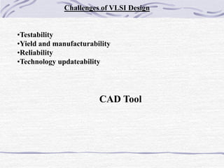
- 29. Challenges of VLSI Design •Testability •Yield and manufacturability •Reliability •Technology updateability CAD Tool