Ch2 microcontroller architecture
2 likes3,006 views

The document discusses the architecture and assembly language programming of PIC18 microcontrollers. It covers topics such as: - PIC18 microcontrollers use a Harvard architecture with separate memory for instructions and data. They have a program memory, data memory, I/O ports, and support devices like timers. - The PIC18 architecture is based on an advanced RISC design. Key components include registers like WREG for temporary data storage. Special function registers and general purpose registers are used to access I/O ports and timers. - Assembly language instructions like MOVLW, ADDLW, and MOVWF are used to move data between program memory, registers and I/O ports. The


Ch2 microcontroller architecture
- 1. Copyright Politeknik Kota Bharu Page 1 CHAPTER 2 – MICROCONTROLLER ARCHITECTURE & ASSEMBLY LANGUAGE PROGRAMMING PIC18 Microcontroller families PIC is a family of modified Harvard architecture microcontrollers made by Microchip Technology, derived from the PIC1650 originally developed by General Instrument's Microelectronics Division. The name PIC initially referred to "Peripheral Interface Controller". 1989 – Microchip Technology Corporation introduced it’s first 8-bit microcontroller PIC18 Architecture PIC microcontrollers are based on advanced RISC architecture. RISC stands for Reduced Instruction Set Computing. In this architecture, the instruction set of hardware gets reduced which increases the execution rate (speed) of system. CPUs use many register to store data temporarily. To program in Assembly Language, we must understand the register and architecture PIC microcontrollers follow Harvard architecture for internal data transfer PIC microcontrollers are designed using the Harvard Architecture which includes: Microprocessor unit (MPU) Program memory for instructions Data memory for data I/O ports Support devices such as timers
- 2. Copyright Politeknik Kota Bharu Page 2
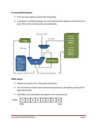
- 3. Copyright Politeknik Kota Bharu Page 3 The data RAM file Register CPUs use many registers to store data temporarily. To program in assembly language, we must understand the registers and architecture of given CPU and the role they play in processing data. WREG register Registers are used to store information temporarily The information could be a byte of data to be processed, or and address pointing to the data to be fetched The WREG is the most widely used register in PIC microcontroller
- 4. Copyright Politeknik Kota Bharu Page 4 The 8-bit WREG register is the most widely used register in the PIC micro controller. WREG stands for working register, as there is only one. The WREG register is the same as the accumulator in other microprocessors. The WREG register is used for all arithmetic and logic instructions. To understand the use of the WREG register, we will show it in the context of two simple instructions: MOVLW and ADDWL. MOVLW Instruction Notice that in MOVLW, the letter L (literal) comes first and then the letter W (WREG), which means "move a literal value to WREG, " the destination. The following instruction loads the WREG register with a literal value of 25H (i.e., 25 in hex). o MOVLW 25H ; move value 25H into WREG o MOVLW 87H ; load 87H into WREG ADDLW Instruction The ADD instruction tells the CPU to add the literal value K to register WREG and put the result back in the WREG register. Notice that in ADDLW, first comes the letter L (literal) and then the letter W (WREG), which means "add a literal value to WREG," the destination MOVLW 25H ; load 25H into WREG ADDLW 34H ; add value 34 to WREG W = W + 34H Executing the above lines results in WREG = 59H (25H + 34H = 59H) File register (SFRs and GPR) File Register (data RAM) is read/write memory used by CPU for data storage, scratch pad and register for internal use and function Divided into two sections: o SFRs – Special Function Registers o GPR – General-Purpose Register
- 5. Copyright Politeknik Kota Bharu Page 5 Special Function Register (SFRs) Special-Function registers are RAM memory locations, their purpose is predetermined during manufacturing process and cannot be changed. Dedicated to specific functions – ALU status, timers, serial communication, I/O ports ADC etc. Fixed by CPU designer at the time of design 8 bits register
- 6. Copyright Politeknik Kota Bharu Page 6 General Purpose Register (GPR) 8-bit registers are a group of RAM locations in the file register that are used for data storage and scratch pad. the space that is not allocated to the SFRs typically used for general-purpose registers MOVWF Instruction Notice that in MOVWF, the letter F stands for a location in the file register, while W means WREG. The MOVWF instructions tells the CPU to move (in reality, copy) the source register of WREG to a destination in the file register (F) MOVLW 55H ; WREG = 55H MOVWF PORTB ; Copy WREG to Port B (Port B = 55H) MOVWF PORTC ; Copy WREG to Port C (Port C = 55H) MOVWF PORTD ; Copy WREG to Port D (Port D = 55H)
- 7. Copyright Politeknik Kota Bharu Page 7 MOVF Instruction The MOVF mnemonic is intended to perform MOVFW. It move the contents of file register into WREG or to itself MOVF PORTB,W ; move from file register of Port B to WREG MOVF PORTB,0 ; move content of file register into WREG MOVF PORTB,1 ; move content of file register into itself Review Question 1. State five example of SFR 2. What is GPR 3. Write an instruction to move value of 58H into WREG 4. Write an instruction to move value of 58H into PORTB 5. What is the difference between the MOVWF and MOVF instruction 6. Explain each instruction below: a. MOVLW 55H b. MOVF PORTB,W Status Register One of the most important register in PIC. Most of PIC has this register. 8-Bit register. Sometime referred as flag register. Only 5 bits of it are used by the PIC18. o called conditional flags The three unused bits are unimplemented and read as 0.
- 8. Copyright Politeknik Kota Bharu Page 8 C (Carry/Borrow Flag) set when an addition generates a carry and a subtraction generates a borrow. DC(Digit Carry Flag):also called Half Carry flag;set when carry generated from Bit3 to Bit4 an arithmetic operatio.n Z(Zero Flag):set when result of an operation is zero. OV(Overflow Flag):set when result of an operation of signed numbers goes beyond seven bits-if the results fall outside 127(0x7F)and -128(0x80). N(Negative Flag):set when bit B7 is one of the result of an arithmetic/logic operation. Example 1. Show the status of the C, DC and Z flag after the addition of 38H and 2FH. Solution: 38H 00111000 + 2FH + 00101111 67H 01100111 C = 0 ; DC = 1; Z = 0
- 9. Copyright Politeknik Kota Bharu Page 9 2. Show the status of the C, DC and Z flags after the addition of 9CH and 64H in the following instructions: MOVLW 9CH ADDLW 64H 3. Write the instruction for addition operation of 88H and 93H and show the status of the C, DC and Z flags. Solution: MOVLW 88H ADDLW 93H Review Question 1. Determine the state of status register after the instruction below: a. MOVLW 0F5H ADDLW 0BH b. MOVLW 9FH ADDLW 61H
- 10. Copyright Politeknik Kota Bharu Page 10 2. Show the status of the C, DC and Z flags after the addition of 9CH and 64H in the following instructions: a. MOVLW 9CH ADDLW 64H b. MOVLW 67H ADDLW 99H c. MOVLW 87H ADDLW 22H Data format and directives PIC data type has only one data type. 8-bits. Size of register also 8-bits ( 00-FF, or 0-255) Data format representation. o Hex, o Binary, o Decimal, o ASCII HEX number Use h, or H right after the number. Example MOVLW 12H Put 0x. Example MOVLW 0x12; Put nothing. Eg. MOVLW 12 Put h in front of number. MOVLW h’12’ Binary number Only one way to represent binary numbers, Example: MOVLW B’00010010’ 1 2 in hex Decimal number Two ways to represent. MOVLW D’12’ , (in hex 0x0C) Or MOVLW .12
- 11. Copyright Politeknik Kota Bharu Page 11 ASCII code To represent ASCII data in PIC assemble we use the letter A as follows MOVLW A’2’ ; WREG = 00110010 or 32 in hex ( see ASCII chart) MOVLW A’c’ ; WREG = 01100011 or 63 in hex (see ASCII chart) MOVLW ‘9’ ; WREG = 39H another way for ASCII
- 12. Copyright Politeknik Kota Bharu Page 12 ASSEMBLER Directive Directive give direction to he assembler.. Example EQU, ORG, END, #INCLUDE, LIST, _CONFIG EQU (equate) Used to define constant value or fixed address. Associates a constant number / address label Eg. COUNT EQU 0x25 MOVLW COUNT ; WREG = 25 ORG (Origin) Indicate the beginning of the address. Example ORG 0x00 END Important to indicate End of code, last line LIST Indicates to the assembler the specific PIC chip for which the program should be assembled. Eg. LIST P=18F458 #INLCUDE Tell the assembler to use the libraries associated with the specific chip _CONFIG To configure bits for the targeted PIC. Read during the power-up, wrong configuration makes PIC unusable.
- 13. Copyright Politeknik Kota Bharu Page 13 Example code Instruction set of PIC18 PIC18F2455/2550/4455/4550 devices incorporate the standard set of 75 PIC18 core instructions. The instruction set is highly orthogonal and is grouped into four basic categories: o Byte-oriented operations o Bit-oriented operations o Literal operations o Control operations
- 14. Copyright Politeknik Kota Bharu Page 14
- 15. Copyright Politeknik Kota Bharu Page 15 Arithmetic Instruction and Operation a. Addition and subtraction MOVLW 0xF5 ; WREG = F5 ADDLW 0x0B ; WREG = F5 + 0B = 00 and C = 1 MOVLW 0x23 ; WREG = 23H SUBLW 0x3F ; WREG = 3F - WREG
- 16. Copyright Politeknik Kota Bharu Page 16 b. Multiplication The PIC supports byte-by-byte multiplication only. The byte is assumed to be unsigned data. The syntax is as follows. After multiplication, the result is in the special function registers PRODH and PRODL; the lower byte is in PRODL, and the upper byte is in PRODH. MULLW K ; W x K 16 bit is result in PRODH:PRODL
- 17. Copyright Politeknik Kota Bharu Page 17 c. Addition of BCD data BCD stands for binary coded decimal. BCD is needed because in everyday life we use the digits 0 to 9 for number, not binary or hex number Binary representation of 0 to 9 is called BCD . In computer literature, one encounters two terms for BCD numbers: (i) unpacked BCD, and (ii) packed BCD. In unpacked BCD, the lower 4 bits of the number represent the BCD number, and the rest of the bits are O. Example: "0000 100 I" and "0000 0101" are unpacked BCD for 9 and 5, respectively. Unpacked BCD requires I byte of memory, or an S-bit register, to contain it. In packed BCD, a single byte has two BCD numbers in it: one in the lower 4 bits, and one in the upper 4 bits. For example, "0101 1001" is packed BCD for 59H. Only I byte of memory is needed to store the packed BCD operands. One reason to use packed BCD is that it is twice as efficient in storing data. There is a problem with adding BCD numbers, which must be corrected. The problem is that after adding packed BCD numbers, the result is no longerBCD. Look at the following. MOVLW 0x17 ADDLW 0x28 Adding these two numbers gives 0011 IIII B (3FH), which is not BCD. A BCD number can only have digits from 0000 to 1001 (or 0 to 9). The result above should have been 17 + 28 = 45 (01000101). To correct this problem, the programmer must add 6 (0 II 0) to the low digit: 3F + 06 = 45H. The same problem could have happened in the upper digit (for example, in 52H + 87H = D9H). Again, 6 must be added to the upper digit (D9H + 60H = 139H) to ensure that the result is BCD (52 + 87 = 139). This problem is so pervasive that most microprocessors such as the PIC 18 have an instruction to deal with it. In the PIC 18 instruction "DAW" is designed to correct the BCD addition problem. The DAW (decimal adjust WREG) instruction in the PIC 18 is provided to correct the aforementioned problem associated with BCD addition. The mnemonic "DAW" works only with an operand in the WREG register. The DAW instruction will add 6 to the lower nibble or higher nibble if needed; otherwise, it will leave the result alone. The following example will clarify these points
- 18. Copyright Politeknik Kota Bharu Page 18 Logic Instruction and Bit Manipulation Apart from I/O and arithmetic instructions, logic instructions are some of most widely used instructions. Boolean logic instructions such as AND, OR, Exclusive-OR (XOR), and complement. Logical operations are useful for looking for array elements with certain properties (e.g., divisible by power of 2) and manipulating I/O pin values (e.g., set certain pins to high, clear a few pins, toggle a few signals, and so on). The logical instruction allow user to perform AND, OR, exclusive-OR and complementing on 8-bit numbers. AND ANDLW K ; WREG = WREG AND K Example : Show the result of the following MOVLW 0x35h ANDLW 0x0Fh
- 19. Copyright Politeknik Kota Bharu Page 19 OR IORLW K ; WREG = WREG OR K Example : Show the result of the following MOVLW 0x04h IORLW 0x30h EX-OR XORLW K ; WREG = WREG XOR K Example : Show the result of the following MOVLW 0x54h XORLW 0x78h
- 20. Copyright Politeknik Kota Bharu Page 20 COMF (Compliment file register) This instruction complements the contents of a file register. The complement action changes the 0s to 1s and the 1s to 0s. This is also called 1’s complement Bit Manipulation BCF – Bit Clear File register (set the bit: bit = 1) BSF – Bit Set File register (clear the bit: bit = 0) BTG – Bit Toggle File register (complement the bit) BTFSC – Bit Test File register, skip if clear (skip next instruction if bit = 0) BTFSS– Bit Test File register, skip if set (skip next instruction if bit = 1) RRNCF – Rotate right f (no carry) RLNCF – Rotate left f (no carry) RRCF – Rotate right f through carry RLCF – Rotate left f through carry Example
- 21. Copyright Politeknik Kota Bharu Page 21 Review Question 1. Explain each of the register below: a. WREG Register b. File Register c. Status Register 2. Include directive is used to …………… 3. EQU is used to ……………………………… 4. Illustrate the result after the following code is executed