301378156 design-of-sram-in-verilog
Download as DOCX, PDF7 likes9,657 views

This document provides an overview of the design of a dual port SRAM using Verilog HDL. It begins with an introduction describing the objectives and accomplishments of the project. It then reviews relevant literature on SRAM design. The document describes the FPGA design flow and introduces Verilog. It provides the design and operation of the SRAM, and discusses simulation results and conclusions. The proposed 8-bit dual port SRAM utilizes negative bitline techniques during write operations to improve write ability and reduce power consumption and area compared to conventional designs.


![a. Wrote a self checking test bench consisting of a driver, monitor,
checker components in verilog.
b. Applied different test cases for the multiplier in the
driver section of the test bench and performed
behavioral simulation for the top level module.
5. Synthesis Phase
a. Performed logic synthesis, Translate, Map, Place and
Route processes and synthesis report is generated.
CHAPTER 2
LITERATURE REVIEW
Semiconductor memory is an electronic data storage device, often used as computer
memory, implemented on a semiconductor-based integrated circuit. It is made in
many different types and technologies.
Semiconductor memory has the property of random access, which means that it takes
the same amount of time to access any memory location, so data can be efficiently
accessed in any random order.[1] This contrasts with data storage media such as hard
disks and CDs which read and write data consecutively and therefore the data can
only be accessed in the same sequence it was written. Semiconductor memory also
has much faster access times than other types of data storage; a byte of data can be
written to or read from semiconductor memory within a few nanoseconds, while
access time for rotating storage such as hard disks is in the range of milliseconds. For
these reasons it is used for main computer memory (primary storage), to hold data the
computer is currently working on, among other uses.](https://image.slidesharecdn.com/301378156-design-of-sram-in-verilog-161010074603/85/301378156-design-of-sram-in-verilog-7-320.jpg)
![Shift registers, processor registers, data buffers and other small digital registers that
have no memory address decoding mechanism are not considered as memory
although they also store digital data.
1.1 Description
In a semiconductor memory chip, each bit of binary data is stored in a tiny circuit
called a memory cell consisting of one to several transistors. The memory cells are
laid out in rectangular arrays on the surface of the chip. The 1-bit memory cells are
grouped in small units called words which are accessed together as a single memory
address. Memory is manufactured in word length that is usually a power of two,
typically N=1, 2, 4 or 8 bits.
Data is accessed by means of a binary number called a memory address applied to the
chip's address pins, which specifies which word in the chip is to be accessed. If the
memory address consists of M bits, the number of addresses on the chip is 2M, each
containing an N bit word. Consequently, the amount of data stored in each chip is
N2M bits.[1] The data capacity is usually a power of two: 2, 4, 8, 16, 32, 64, 128, 256
and 512 and measured in kibibits, mebibits, gibibits or tebibits, etc. Currently (2014)
the largest semiconductor memory chips hold a few gibibits of data, but higher
capacity memory is constantly being developed. By combining several integrated
circuits, memory can be arranged into a larger word length and/or address space than
what is offered by each chip, often but not necessarily a power of two.[1]
The two basic operations performed by a memory chip are "read", in which the data
contents of a memory word is read out (nondestructively), and "write" in which data is
stored in a memory word, replacing any data that was previously stored there. To
increase data rate, in some of the latest types of memory chips such as DDR SDRAM
multiple words are accessed with each read or write operation.
In addition to standalone memory chips, blocks of semiconductor memory are integral
parts of many computer and data processing integrated circuits. For example the
microprocessor chips that run computers contain cache memory to store instructions
awaiting execution.](https://image.slidesharecdn.com/301378156-design-of-sram-in-verilog-161010074603/85/301378156-design-of-sram-in-verilog-8-320.jpg)
![1.2 Types
RAM chips for computers usually come on removable memory modules like these.
Additional memory can be added to the computer by plugging in additional modules.
RAM (Random access memory) has become a generic term for any semiconductor
memory that can be written to, as well as read from, in contrast to ROM (below),
which can only be read. All semiconductor memory, not just RAM, has the property
of random access.
Volatile memory loses its stored data when the power to the memory chip is turned
off. However it can be faster and less expensive than non-volatile memory. This type
is used for the main memory in most computers, since data is stored on the hard disk
while the computer is off. Major types are:[2][3]
DRAM (Dynamic random-access memory) which uses memory cells
consisting of one capacitor and one transistor to store each bit. This is the
cheapest and highest in density, so it is used for the main memory in
computers. However the electric charge that stores the data in the memory
cells slowly leaks off, so the memory cells must be periodically refreshed
(rewritten), requiring additional circuitry. The refresh process is automatic and
transparent to the user.](https://image.slidesharecdn.com/301378156-design-of-sram-in-verilog-161010074603/85/301378156-design-of-sram-in-verilog-9-320.jpg)

![ RDRAM (Rambus DRAM) an alternate double data rate
memory standard that was used on some Intel systems but
ultimately lost out to DDR SDRAM.
SGRAM (Synchronous graphics RAM) a specialized type of
SDRAM made for graphics adaptors (video cards). It can
perform graphics-related operations such as bit masking and
block write, and can open two pages of memory at once.
PSRAM (Pseudostatic RAM) This is DRAM which has
circuitry to perform memory refresh on the chip, so that it acts
like SRAM, allowing the external memory controller to be shut
down to save energy. It is used in a few portable game
controllers such as the Wii.
SRAM (Static random-access memory) which relies on several transistors
forming a digital flip-flop to store each bit. This is less dense and more
expensive per bit than DRAM, but faster and does not require memory refresh.
It is used for smaller cache memories in computers.
Content-addressable memory This is a specialized type in which, instead of
accessing data using an address, a data word is applied and the memory
returns the location if the word is stored in the memory. It is mostly
incorporated in other chips such as microprocessors where it is used for cache
memory.
Nonvolatile memory preserves the data stored in it during periods when the power to
the chip is turned off. Therefore it is used for the memory in portable devices, which
don't have disks, and for removable memory cards among other uses. Major types
are:[2][3]
ROM (Read-only memory) This is designed to hold permanent data, and in
normal operation is only read from, not written to. Although many types can
be written to, the writing process is slow and usually all the data in the chip
must be rewritten at once. It is usually used to store system software which
must be immediately accessible to the computer, such as the BIOS program
which starts the computer, and the software (microcode) for portable devices
and embedded computers such as microcontrollers.](https://image.slidesharecdn.com/301378156-design-of-sram-in-verilog-161010074603/85/301378156-design-of-sram-in-verilog-11-320.jpg)

![Static random-access memory (SRAM or static RAM) is a type of semiconductor
memory that uses bistable latching circuitry to store each bit. The term static
differentiates it from dynamic RAM (DRAM) which must be periodically refreshed.
SRAM exhibits data remanence,[1] but it is still volatile in the conventional sense that
data is eventually lost when the memory is not powered.
1.3 Applications and uses
SRAM cells on the die of a STM32F103VGT6 microcontroller as seen by a scanning
electron microscope. Manufactured by STMicroelectronics using a 180 nanometre
process.
Comparison image of 180 nanometre SRAM cells on a STM32F103VGT6
microcontroller as seen by an optical microscope.
1.3.1 Characteristics
SRAM is more expensive and less dense than DRAM and is therefore not used
for high-capacity, low-cost applications such as the main memory in personal
computers.
1.3.1.1 Clock rate and power
The power consumption of SRAM varies widely depending on how frequently it is
accessed; it can be as power-hungry as dynamic RAM, when used at high
frequencies, and some ICs can consume many watts at full bandwidth. On the other
hand, static RAM used at a somewhat slower pace, such as in applications with](https://image.slidesharecdn.com/301378156-design-of-sram-in-verilog-161010074603/85/301378156-design-of-sram-in-verilog-13-320.jpg)
![moderately clocked microprocessors, draws very little power and can have a nearly
negligible power consumption when sitting idle – in the region of a few micro-watts.
Static RAM exists primarily as:
general purpose products
o with asynchronous interface, such as the ubiquitous 28-pin 8K × 8 and
32K × 8 chips (often but not always named something along the lines
of 6264 and 62C256 respectively), as well as similar products up to
16 Mbit per chip
o with synchronous interface, usually used for caches and other
applications requiring burst transfers, up to 18 Mbit (256K × 72) per
chip
integrated on chip
o as RAM or cache memory in micro-controllers (usually from around
32 bytes up to 128 kilobytes)
o as the primary caches in powerful microprocessors, such as the x86
family, and many others (from 8 KB, up to many megabytes)
o to store the registers and parts of the state-machines used in some
microprocessors (see register file)
o on application specific ICs, or ASICs (usually in the order of kilobytes)
o in FPGAs and CPLDs
1.3.1.2 Embedded use
Many categories of industrial and scientific subsystems, automotive
electronics, and similar, contain static RAM.
Some amount (kilobytes or less) is also embedded in practically all modern
appliances, toys, etc. that implement an electronic user interface.
Several megabytes may be used in complex products such as digital cameras,
cell phones, synthesizers, etc.
SRAM in its dual-ported form is sometimes used for realtime digital signal processing
circuits.[citation needed]](https://image.slidesharecdn.com/301378156-design-of-sram-in-verilog-161010074603/85/301378156-design-of-sram-in-verilog-14-320.jpg)
![1.3.1.3 In computers
SRAM is also used in personal computers, workstations, routers and peripheral
equipment: CPU register files, internal CPU caches and external burst mode SRAM
caches, hard disk buffers, router buffers, etc. LCD screens and printers also normally
employ static RAM to hold the image displayed (or to be printed).
1.3.1.4 Hobbyists
Hobbyists, specifically homebuilt processor enthusiasts,[2] often prefer SRAM due to
the ease of interfacing. It is much easier to work with than DRAM as there are no
refresh cycles and the address and data buses are directly accessible rather than
multiplexed. In addition to buses and power connections, SRAM usually requires only
three controls: Chip Enable (CE), Write Enable (WE) and Output Enable (OE). In
synchronous SRAM, Clock (CLK) is also included.[citation needed]
1.4 Types of SRAM
1.4.1 Non-volatile SRAM
Non-volatile SRAMs, or nvSRAMs, have standard SRAM functionality, but they save
the data when the power supply is lost, ensuring preservation of critical information.
nvSRAMs are used in a wide range of situations—networking, aerospace, and
medical, among many others[3] —where the preservation of data is critical and where
batteries are impractical.
1.4.2 Asynchronous SRAM
Asynchronous SRAM are available from 4 Kb to 64 Mb. The fast access time of
SRAM makes asynchronous SRAM appropriate as main memory for small cache-less
embedded processors used in everything from industrial electronics and measurement
systems to hard disks and networking equipment, among many other applications.
They are used in various applications like switches and routers, IP-Phones, IC-
Testers, DSLAM Cards, to Automotive Electronics.](https://image.slidesharecdn.com/301378156-design-of-sram-in-verilog-161010074603/85/301378156-design-of-sram-in-verilog-15-320.jpg)

![Chapter 3
DESIGN OF SRAM IN VERILOG
3.1 Design of SRAM
A typical SRAM cell is made up of six MOSFETs. Each bit in an SRAM is stored on
four transistors (M1, M2, M3, M4) that form two cross-coupled inverters. This
storage cell has two stable states which are used to denote 0 and 1. Two additional
access transistors serve to control the access to a storage cell during read and write
operations. In addition to such six-transistor (6T) SRAM, other kinds of SRAM chips
use 4, 8, 10 (4T, 8T, 10T SRAM), or more transistors per bit.[4][5][6] Four-transistor](https://image.slidesharecdn.com/301378156-design-of-sram-in-verilog-161010074603/85/301378156-design-of-sram-in-verilog-17-320.jpg)
![SRAM is quite common in stand-alone SRAM devices (as opposed to SRAM used for
CPU caches), implemented in special processes with an extra layer of polysilicon,
allowing for very high-resistance pull-up resistors. [7] The principal drawback of using
4T SRAM is increased static power due to the constant current flow through one of
the pull-down transistors.
Four transistor SRAM provides advantages in density at the cost of manufacturing
complexity. The resistors must have small dimensions and large values.
This is sometimes used to implement more than one (read and/or write) port, which
may be useful in certain types of video memory and register files implemented with
multi-ported SRAM circuitry.
Generally, the fewer transistors needed per cell, the smaller each cell can be. Since the
cost of processing a silicon wafer is relatively fixed, using smaller cells and so
packing more bits on one wafer reduces the cost per bit of memory.](https://image.slidesharecdn.com/301378156-design-of-sram-in-verilog-161010074603/85/301378156-design-of-sram-in-verilog-18-320.jpg)
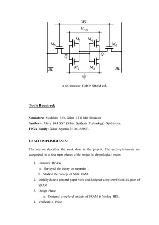
![A six-transistor CMOS SRAM cell.
Memory cells that use fewer than four transistors are possible – but, such 3T[8][9] or 1T
cells are DRAM, not SRAM (even the so-called 1T-SRAM).
Access to the cell is enabled by the word line (WL in figure) which controls the two
access transistors M5 and M6 which, in turn, control whether the cell should be
connected to the bit lines: BL and BL. They are used to transfer data for both read and
write operations. Although it is not strictly necessary to have two bit lines, both the
signal and its inverse are typically provided in order to improve noise margins.
During read accesses, the bit lines are actively driven high and low by the inverters in
the SRAM cell. This improves SRAM bandwidth compared to DRAMs – in a
DRAM, the bit line is connected to storage capacitors and charge sharing causes the
bitline to swing upwards or downwards. The symmetric structure of SRAMs also
allows for differential signaling, which makes small voltage swings more easily
detectable. Another difference with DRAM that contributes to making SRAM faster is
that commercial chips accept all address bits at a time. By comparison, commodity
DRAMs have the address multiplexed in two halves, i.e. higher bits followed by
lower bits, over the same package pins in order to keep their size and cost down.
The size of an SRAM with m address lines and n data lines is 2m words, or 2m × n
bits. The most common word size is 8 bits, meaning that a single byte can be read or](https://image.slidesharecdn.com/301378156-design-of-sram-in-verilog-161010074603/85/301378156-design-of-sram-in-verilog-19-320.jpg)


![confused with VHDL (a competing language), is most commonly used in the design,
verification, and implementation ofdigital logic chips at the register-transfer
level of abstraction. It is also used in the verification ofanalog and mixed-signal
circuits.
1.5 Overview
Hardware description languages such as Verilog differ from
software programming languages because they include ways of describing the
propagation of time and signal dependencies (sensitivity). There are two assignment
operators, a blocking assignment (=), and a non-blocking (<=) assignment. The non-
blocking assignment allows designers to describe a state-machine update without
needing to declare and use temporary storage variables (in any general programming
language we need to define some temporary storage spaces for the operands to be
operated on subsequently; those are temporary storage variables). Since these
concepts are part of Verilog's language semantics, designers could quickly write
descriptions of large circuits in a relatively compact and concise form. At the time of
Verilog's introduction (1984), Verilog represented a tremendous productivity
improvement for circuit designers who were already using graphical schematic
capturesoftware and specially-written software programs to document and simulate
electronic circuits.
The designers of Verilog wanted a language with syntax similar to the C
programming language, which was already widely used in engineering software
development. Verilog is case-sensitive, has a basic preprocessor (though less
sophisticated than that of ANSI C/C++), and equivalent control
flow keywords (if/else, for, while, case, etc.), and compatible operator precedence.
Syntactic differences include variable declaration (Verilog requires bit-widths on
net/reg types[clarification needed]), demarcation of procedural blocks (begin/end instead of
curly braces {}), and many other minor differences.
A Verilog design consists of a hierarchy of modules. Modules
encapsulate design hierarchy, and communicate with other modules through a set of
declared input, output, and bidirectional ports. Internally, a module can contain any
combination of the following: net/variable declarations (wire, reg, integer, etc.),
concurrent and sequential statement blocks, and instances of other modules (sub-](https://image.slidesharecdn.com/301378156-design-of-sram-in-verilog-161010074603/85/301378156-design-of-sram-in-verilog-52-320.jpg)


![input rst; // These inputs/outputs represent
input clk; // connections to the module.
input cet;
input cep;
output [size-1:0] count;
output tc;
reg [size-1:0] count; // Signals assigned
// within an always
// (or initial)block
// must be of type reg
wire tc; // Other signals are of type wire
// The always statement below is a parallel
// execution statement that
// executes any time the signals
// rst or clk transition from low to high
always @ (posedge clk or posedge rst)
if (rst) // This causes reset of the cntr
count <= {size{1'b0}};
else
if (cet && cep) // Enables both true
begin
if (count == length-1)
count <= {size{1'b0}};
else
count <= count + 1'b1;
end
// the value of tc is continuously assigned
// the value of the expression](https://image.slidesharecdn.com/301378156-design-of-sram-in-verilog-161010074603/85/301378156-design-of-sram-in-verilog-58-320.jpg)


Ad
More Related Content
What's hot (20)
Similar to 301378156 design-of-sram-in-verilog (20)


Ad
Recently uploaded (20)


Ad
301378156 design-of-sram-in-verilog
- 1. Design Of Dual Port SRAM Using Verilog HDL TABLE OF CONTENTS
- 2. List of figures List of tables Chapter 1 INTRODUCTION 1.1 Design Objectives 1.2 ACCOMPLISHMENTS Chapter 2 LITERATURE REVIEW Chapter 3 3.1 DesignofSRAM 3.2 SRAM Operation Chapter 4 Introduction to FPGA design Flow 4.1 INTRODUCTION TO VLSI & FPGA DESIGN FLOW 4.1.1 Design Entry 4.1.2 Synthesis 4.1.3. Implementation 4.1.3.1 Translate 4.1.3.2 Map 4.1.3.3 Place and Route
- 3. 4.1.4 Device Programming 4.1.5 Design Verification 4.1.6 Behavioral Simulation 4.1.7 Functional simulation 4.1.8. Static Timing Analysis Chapter 5 VERILOG INTRODUCTION Chapter 6 Simulation Results Chapter 7 Conclusion and Future Scope Bibliography and References
- 4. ABSTRACT Low power and low area Static Random Access Memory (SRAM) is essential for System on Chip (SoC) technology. Dual-Port (DP) SRAM greatly reduces the power consumption by full current-mode techniques for read/write operation and the area by using Single-Port (SP) cell. An 8 bit DP-SRAM is proposed in this study. Negative bit-line technique during write has been utilized for write-assist solutions. Negative voltage is generated on-chip using capacitive coupling. The proposed circuit design topology does not affect the read operation for bit interleaved architectures enabling high-speed operation. Designed in XILINX ISE 14.4 Simulation results and comparative study of the present scheme with state of-the art conventional schemes proposed .show that the proposed scheme is superior in terms of process-variations impact, area overhead, timings and dynamic power consumption. The proposed negative bitline technique can be used to improve the write ability of 6 T Single-Port (SP) as well as 8 T DP and other multiport SRAM cells.
- 5. CHAPTER 1 INTRODUCTION Most systems contain the following kinds of memories: •PROM • EPROM • EEPROM/Flash • DRAM •SRAM PROMs, EPROMs, and Flash memories come under the cat- egory of nonvolatile memories. Nonvolatile memories are devices that will store data even when the power to the device is removed. PROMs, EPROMs, and Flash memories differ in the technology used and method by which the user reprograms the device and the method by which the user erases the data in the memory device. SRAM and DRAM are random access memories, that can store data as long as power is applied to the device. If the power is ever removed, all data that was stored in the mem- ory will be lost. Even when powered, in DRAMs data could be lost if it is not periodically refreshed; while in SRAMs the data can be stored without any kind of extra processing or refresh- ing. The data will remain in t he SRAM once it has been writ- ten there, as long as the power supply to the device is maintained. SRAMs are differentiated from their other memory counter- parts by the type of the memory cell. Nearly all SRAMs either use a 4-transistor or a 6-tran sistor Memory Cell. These cell structures allow data to be stored for an indefinite amount of time in the device as long as it is powered. Figure 1below shows the 4-transistor and the 6-transistor cell. (These are usually referred to as the 4-T and the 6-T cells, respectively.) The SRAM cell is formed by two cross-coupled inverters. System evolution over time has led to the creation of different types of SRAMs. The next section goes into the details of the different kinds of SRAMs and their applications.
- 6. A six-transistor CMOS SRAM cell. Tools Required: Simulators: Modelsim 6.5b, Xilinx 12.1i Isim Simulator Synthesis: Xilinx 14.4 XST (Xilinx Synthesis Technology) Synthesizer. FPGA Family: Xilinx Spartan 3E XC3S500E. 1.2 ACCOMPLISHMENTS: This section describes the work done in the project. The accomplishments are categorized in to four main phases of the project in chronological order: 1. Literature Review a. Surveyed the theory on memories . b. Studied the concept of Static RAM. 2. Initially done a pen and paper work and designed a top level block diagram of SRAM 3. Design Phase a. Designed a top level module of SRAM in Verilog HDL. 4. Verification Phase
- 7. a. Wrote a self checking test bench consisting of a driver, monitor, checker components in verilog. b. Applied different test cases for the multiplier in the driver section of the test bench and performed behavioral simulation for the top level module. 5. Synthesis Phase a. Performed logic synthesis, Translate, Map, Place and Route processes and synthesis report is generated. CHAPTER 2 LITERATURE REVIEW Semiconductor memory is an electronic data storage device, often used as computer memory, implemented on a semiconductor-based integrated circuit. It is made in many different types and technologies. Semiconductor memory has the property of random access, which means that it takes the same amount of time to access any memory location, so data can be efficiently accessed in any random order.[1] This contrasts with data storage media such as hard disks and CDs which read and write data consecutively and therefore the data can only be accessed in the same sequence it was written. Semiconductor memory also has much faster access times than other types of data storage; a byte of data can be written to or read from semiconductor memory within a few nanoseconds, while access time for rotating storage such as hard disks is in the range of milliseconds. For these reasons it is used for main computer memory (primary storage), to hold data the computer is currently working on, among other uses.
- 8. Shift registers, processor registers, data buffers and other small digital registers that have no memory address decoding mechanism are not considered as memory although they also store digital data. 1.1 Description In a semiconductor memory chip, each bit of binary data is stored in a tiny circuit called a memory cell consisting of one to several transistors. The memory cells are laid out in rectangular arrays on the surface of the chip. The 1-bit memory cells are grouped in small units called words which are accessed together as a single memory address. Memory is manufactured in word length that is usually a power of two, typically N=1, 2, 4 or 8 bits. Data is accessed by means of a binary number called a memory address applied to the chip's address pins, which specifies which word in the chip is to be accessed. If the memory address consists of M bits, the number of addresses on the chip is 2M, each containing an N bit word. Consequently, the amount of data stored in each chip is N2M bits.[1] The data capacity is usually a power of two: 2, 4, 8, 16, 32, 64, 128, 256 and 512 and measured in kibibits, mebibits, gibibits or tebibits, etc. Currently (2014) the largest semiconductor memory chips hold a few gibibits of data, but higher capacity memory is constantly being developed. By combining several integrated circuits, memory can be arranged into a larger word length and/or address space than what is offered by each chip, often but not necessarily a power of two.[1] The two basic operations performed by a memory chip are "read", in which the data contents of a memory word is read out (nondestructively), and "write" in which data is stored in a memory word, replacing any data that was previously stored there. To increase data rate, in some of the latest types of memory chips such as DDR SDRAM multiple words are accessed with each read or write operation. In addition to standalone memory chips, blocks of semiconductor memory are integral parts of many computer and data processing integrated circuits. For example the microprocessor chips that run computers contain cache memory to store instructions awaiting execution.
- 9. 1.2 Types RAM chips for computers usually come on removable memory modules like these. Additional memory can be added to the computer by plugging in additional modules. RAM (Random access memory) has become a generic term for any semiconductor memory that can be written to, as well as read from, in contrast to ROM (below), which can only be read. All semiconductor memory, not just RAM, has the property of random access. Volatile memory loses its stored data when the power to the memory chip is turned off. However it can be faster and less expensive than non-volatile memory. This type is used for the main memory in most computers, since data is stored on the hard disk while the computer is off. Major types are:[2][3] DRAM (Dynamic random-access memory) which uses memory cells consisting of one capacitor and one transistor to store each bit. This is the cheapest and highest in density, so it is used for the main memory in computers. However the electric charge that stores the data in the memory cells slowly leaks off, so the memory cells must be periodically refreshed (rewritten), requiring additional circuitry. The refresh process is automatic and transparent to the user.
- 10. o FPM DRAM (Fast page mode DRAM) An older type of asynchronous DRAM that improved on previous types by allowing repeated accesses to a single "page" of memory to occur at a faster rate. Used in the mid- 1990s. o EDO DRAM (Extended data out DRAM) An older type of asynchronous DRAM which had faster access time than earlier types by being able to initiate a new memory access while data from the previous access was still being transferred. Used in the later part of the 1990s. o VRAM (Video random access memory) An older type of dual-ported memory once used for the frame buffers of video adapters (video cards). o SDRAM (Synchronous dynamic random-access memory) This was a reorganization of the DRAM memory chip, which added a clock line to enable it to operate in synchronism with the computer's memory bus clock. The data on the chip is divided into banks so it can work on several memory accesses simultaneously, in separate banks. It became the dominant type of computer memory by about the year 2000. DDR SDRAM (Double data rate SDRAM) This was an increased data rate modification, enabling the chip to transfer twice the memory data (two consecutive words) on each clock cycle by double pumping, transferring data on both the leading and trailing edges of the clock pulse. Extensions of this idea are the current (2012) technique being used to increase memory access rate and bandwidth. Since it is proving difficult to further increase the internal clock speed of memory chips, these chips increase data rate by transferring data in larger blocks: DDR2 SDRAM transfers 4 consecutive words per internal clock cycle DDR3 SDRAM transfers 8 consecutive words per internal clock cycle. DDR4 SDRAM transfers 16 consecutive words per internal clock cycle. It is scheduled to debut in 2012.
- 11. RDRAM (Rambus DRAM) an alternate double data rate memory standard that was used on some Intel systems but ultimately lost out to DDR SDRAM. SGRAM (Synchronous graphics RAM) a specialized type of SDRAM made for graphics adaptors (video cards). It can perform graphics-related operations such as bit masking and block write, and can open two pages of memory at once. PSRAM (Pseudostatic RAM) This is DRAM which has circuitry to perform memory refresh on the chip, so that it acts like SRAM, allowing the external memory controller to be shut down to save energy. It is used in a few portable game controllers such as the Wii. SRAM (Static random-access memory) which relies on several transistors forming a digital flip-flop to store each bit. This is less dense and more expensive per bit than DRAM, but faster and does not require memory refresh. It is used for smaller cache memories in computers. Content-addressable memory This is a specialized type in which, instead of accessing data using an address, a data word is applied and the memory returns the location if the word is stored in the memory. It is mostly incorporated in other chips such as microprocessors where it is used for cache memory. Nonvolatile memory preserves the data stored in it during periods when the power to the chip is turned off. Therefore it is used for the memory in portable devices, which don't have disks, and for removable memory cards among other uses. Major types are:[2][3] ROM (Read-only memory) This is designed to hold permanent data, and in normal operation is only read from, not written to. Although many types can be written to, the writing process is slow and usually all the data in the chip must be rewritten at once. It is usually used to store system software which must be immediately accessible to the computer, such as the BIOS program which starts the computer, and the software (microcode) for portable devices and embedded computers such as microcontrollers.
- 12. o Mask programmed ROM In this type the data is programmed into the chip during manufacture, so it is only used for large production runs. It cannot be rewritten with new data. o PROM (Programmable read-only memory) In this type the data is written into the chip before it is installed in the circuit, but it can only be written once. The data is written by plugging the chip into a device called a PROM programmer. o EPROM (Erasable programmable read-only memory) In this type the data in it can be rewritten by removing the chip from the circuit board, exposing it to an ultraviolet light to erase the existing data, and plugging it into a PROM programmer. The IC package has a small transparent "window" in the top to admit the UV light. It is often used for prototypes and small production run devices, where the program in it may have to be changed at the factory. 4M EPROM, showing transparent window used to erase the chip o EEPROM (Electrically erasable programmable read-only memory) In this type the data can be rewritten electrically, while the chip is on the circuit board, but the writing process is slow. This type is used to hold firmware, the low level microcode which runs hardware devices, such as the BIOS program in most computers, so that it can be updated. NVRAM (Flash memory) In this type the writing process is intermediate in speed between EEPROMS and RAM memory; it can be written to, but not fast enough to serve as main memory. It is often used as a semiconductor version of a hard disk, to store files. It is used in portable devices such as PDAs, USB flash drives, and removable memory cards used in digital cameras and cellphones.
- 13. Static random-access memory (SRAM or static RAM) is a type of semiconductor memory that uses bistable latching circuitry to store each bit. The term static differentiates it from dynamic RAM (DRAM) which must be periodically refreshed. SRAM exhibits data remanence,[1] but it is still volatile in the conventional sense that data is eventually lost when the memory is not powered. 1.3 Applications and uses SRAM cells on the die of a STM32F103VGT6 microcontroller as seen by a scanning electron microscope. Manufactured by STMicroelectronics using a 180 nanometre process. Comparison image of 180 nanometre SRAM cells on a STM32F103VGT6 microcontroller as seen by an optical microscope. 1.3.1 Characteristics SRAM is more expensive and less dense than DRAM and is therefore not used for high-capacity, low-cost applications such as the main memory in personal computers. 1.3.1.1 Clock rate and power The power consumption of SRAM varies widely depending on how frequently it is accessed; it can be as power-hungry as dynamic RAM, when used at high frequencies, and some ICs can consume many watts at full bandwidth. On the other hand, static RAM used at a somewhat slower pace, such as in applications with
- 14. moderately clocked microprocessors, draws very little power and can have a nearly negligible power consumption when sitting idle – in the region of a few micro-watts. Static RAM exists primarily as: general purpose products o with asynchronous interface, such as the ubiquitous 28-pin 8K × 8 and 32K × 8 chips (often but not always named something along the lines of 6264 and 62C256 respectively), as well as similar products up to 16 Mbit per chip o with synchronous interface, usually used for caches and other applications requiring burst transfers, up to 18 Mbit (256K × 72) per chip integrated on chip o as RAM or cache memory in micro-controllers (usually from around 32 bytes up to 128 kilobytes) o as the primary caches in powerful microprocessors, such as the x86 family, and many others (from 8 KB, up to many megabytes) o to store the registers and parts of the state-machines used in some microprocessors (see register file) o on application specific ICs, or ASICs (usually in the order of kilobytes) o in FPGAs and CPLDs 1.3.1.2 Embedded use Many categories of industrial and scientific subsystems, automotive electronics, and similar, contain static RAM. Some amount (kilobytes or less) is also embedded in practically all modern appliances, toys, etc. that implement an electronic user interface. Several megabytes may be used in complex products such as digital cameras, cell phones, synthesizers, etc. SRAM in its dual-ported form is sometimes used for realtime digital signal processing circuits.[citation needed]
- 15. 1.3.1.3 In computers SRAM is also used in personal computers, workstations, routers and peripheral equipment: CPU register files, internal CPU caches and external burst mode SRAM caches, hard disk buffers, router buffers, etc. LCD screens and printers also normally employ static RAM to hold the image displayed (or to be printed). 1.3.1.4 Hobbyists Hobbyists, specifically homebuilt processor enthusiasts,[2] often prefer SRAM due to the ease of interfacing. It is much easier to work with than DRAM as there are no refresh cycles and the address and data buses are directly accessible rather than multiplexed. In addition to buses and power connections, SRAM usually requires only three controls: Chip Enable (CE), Write Enable (WE) and Output Enable (OE). In synchronous SRAM, Clock (CLK) is also included.[citation needed] 1.4 Types of SRAM 1.4.1 Non-volatile SRAM Non-volatile SRAMs, or nvSRAMs, have standard SRAM functionality, but they save the data when the power supply is lost, ensuring preservation of critical information. nvSRAMs are used in a wide range of situations—networking, aerospace, and medical, among many others[3] —where the preservation of data is critical and where batteries are impractical. 1.4.2 Asynchronous SRAM Asynchronous SRAM are available from 4 Kb to 64 Mb. The fast access time of SRAM makes asynchronous SRAM appropriate as main memory for small cache-less embedded processors used in everything from industrial electronics and measurement systems to hard disks and networking equipment, among many other applications. They are used in various applications like switches and routers, IP-Phones, IC- Testers, DSLAM Cards, to Automotive Electronics.
- 16. 1.4.3 By transistor type Bipolar junction transistor (used in TTL and ECL) – very fast but consumes a lot of power MOSFET (used in CMOS) – low power and very common today 1.4.4 By function Asynchronous – independent of clock frequency; data in and data out are controlled by address transition Synchronous – all timings are initiated by the clock edge(s). Address, data in and other control signals are associated with the clock signals 1.4.5 By feature ZBT (ZBT stands for zero bus turnaround) – the turnaround is the number of clock cycles it takes to change access to the SRAM from write to read and vice versa. The turnaround for ZBT SRAMs or the latency between read and write cycle is zero. syncBurst (syncBurst SRAM or synchronous-burst SRAM) – features synchronous burst write access to the SRAM to increase write operation to the SRAM DDR SRAM – Synchronous, single read/write port, double data rate I/O Quad Data Rate SRAM – Synchronous, separate read and write ports, quadruple data rate I/O
- 17. Chapter 3 DESIGN OF SRAM IN VERILOG 3.1 Design of SRAM A typical SRAM cell is made up of six MOSFETs. Each bit in an SRAM is stored on four transistors (M1, M2, M3, M4) that form two cross-coupled inverters. This storage cell has two stable states which are used to denote 0 and 1. Two additional access transistors serve to control the access to a storage cell during read and write operations. In addition to such six-transistor (6T) SRAM, other kinds of SRAM chips use 4, 8, 10 (4T, 8T, 10T SRAM), or more transistors per bit.[4][5][6] Four-transistor
- 18. SRAM is quite common in stand-alone SRAM devices (as opposed to SRAM used for CPU caches), implemented in special processes with an extra layer of polysilicon, allowing for very high-resistance pull-up resistors. [7] The principal drawback of using 4T SRAM is increased static power due to the constant current flow through one of the pull-down transistors. Four transistor SRAM provides advantages in density at the cost of manufacturing complexity. The resistors must have small dimensions and large values. This is sometimes used to implement more than one (read and/or write) port, which may be useful in certain types of video memory and register files implemented with multi-ported SRAM circuitry. Generally, the fewer transistors needed per cell, the smaller each cell can be. Since the cost of processing a silicon wafer is relatively fixed, using smaller cells and so packing more bits on one wafer reduces the cost per bit of memory.
- 19. A six-transistor CMOS SRAM cell. Memory cells that use fewer than four transistors are possible – but, such 3T[8][9] or 1T cells are DRAM, not SRAM (even the so-called 1T-SRAM). Access to the cell is enabled by the word line (WL in figure) which controls the two access transistors M5 and M6 which, in turn, control whether the cell should be connected to the bit lines: BL and BL. They are used to transfer data for both read and write operations. Although it is not strictly necessary to have two bit lines, both the signal and its inverse are typically provided in order to improve noise margins. During read accesses, the bit lines are actively driven high and low by the inverters in the SRAM cell. This improves SRAM bandwidth compared to DRAMs – in a DRAM, the bit line is connected to storage capacitors and charge sharing causes the bitline to swing upwards or downwards. The symmetric structure of SRAMs also allows for differential signaling, which makes small voltage swings more easily detectable. Another difference with DRAM that contributes to making SRAM faster is that commercial chips accept all address bits at a time. By comparison, commodity DRAMs have the address multiplexed in two halves, i.e. higher bits followed by lower bits, over the same package pins in order to keep their size and cost down. The size of an SRAM with m address lines and n data lines is 2m words, or 2m × n bits. The most common word size is 8 bits, meaning that a single byte can be read or
- 20. written to each of 2m different words within the SRAM chip. Several common SRAM chips have 11 address lines (thus a capacity of 2m = 2,048 = 2k words) and an 8-bit word, so they are referred to as "2k × 8 SRAM". 3.2SRAM operation An SRAM cell has three different states. It can be in: standby (the circuit is idle), reading (the data has been requested) and writing (updating the contents). The SRAM to operate in read mode and write mode should have "readability" and "write stability" respectively. The three different states work as follows: 3.2.1 Standby If the word line is not asserted, the access transistors M5 and M6 disconnect the cell from the bit lines. The two cross-coupled inverters formed by M1 – M4 will continue to reinforce each other as long as they are connected to the supply. 3.2.2 Reading Assume that the content of the memory is a 1, stored at Q. The read cycle is started by precharging both the bit lines to a logical 1, then asserting the word line WL, enabling both the access transistors. The second step occurs when the values stored in Q and Q are transferred to the bit lines by leaving BL at its precharged value and discharging BL through M1 and M5 to a logical 0 (i. e. eventually discharging through the transistor M1 as it is turned on because the Q is logically set to 1). On the BL side, the transistors M4 and M6 pull the bit line toward VDD, a logical 1 (i. e. eventually being charged by the transistor M4 as it is turned on because Q is logically set to 0). If the content of the memory was a 0, the opposite would happen and BL would be pulled toward 1 and BL toward 0. Then the BL and BL lines will have a small voltage difference between them while reaching a sense amplifier, which will sense which line has the higher voltage thus determining whether there was 1 stored or 0. The higher the sensitivity of the sense amplifier, the faster the speed of the read operation. 3.2.3 Writing
- 21. The start of a write cycle begins by applying the value to be written to the bit lines. If we wish to write a 0, we would apply a 0 to the bit lines, i.e. setting BL to 1 and BL to 0. This is similar to applying a reset pulse to an SR-latch, which causes the flip flop to change state. A 1 is written by inverting the values of the bit lines. WL is then asserted and the value that is to be stored is latched in. Note that the reason this works is that the bit line input-drivers are designed to be much stronger than the relatively weak transistors in the cell itself, so that they can easily override the previous state of the cross-coupled inverters. Careful sizing of the transistors in an SRAM cell is needed to ensure proper operation. 1.4.4 Bus behavior RAM with an access time of 70 ns will output valid data within 70 ns from the time that the address lines are valid. But the data will remain for a hold time as well (5– 10 ns). Rise and fall times also influence valid timeslots with approximately 5 ns. By reading the lower part of an address range bits in sequence (page cycle) one can read with significantly shorter access time (30 ns)
- 22. CHAPTER 4 INTRODUCTION TO VLSI & FPGA DESIGN FLOW Introduction to VLSI 4.1 Historical Perspective The electronics industry has achieved a phenomenal growth over the last two decades, mainly due to the rapid advances in integration technologies, large-scale systems design - in short, due to the advent of VLSI. The number of applications of integrated circuits in high-performance computing, telecommunications, and consumer electronics has been rising steadily, and at a very fast pace. Typically, the required computational power (or, in other words, the intelligence) of these applications is the driving force for the fast development of this field. Figure 1.1 gives an overview of the prominent trends in information technologies over the next few decades. The current leading-edge technologies (such as low bit-rate video and cellular communications) already provide the end-users a certain amount of processing power and portability.
- 23. This trend is expected to continue, with very important implications on VLSI and systems design. One of the most important characteristics of information services is their increasing need for very high processing power and bandwidth (in order to handle real-time video, for example). The other important characteristic is that the information services tend to become more and more personalized (as opposed to collective services such as broadcasting), which means that the devices must be more intelligent to answer individual demands, and at the same time they must be portable to allow more flexibility/mobility As more and more complex functions are required in various data processing and telecommunications devices, the need to integrate these functions in a small system/package is also increasing. The level of integration as measured by the number of logic gates in a monolithic chip has been steadily rising for almost three decades, mainly due to the rapid progress in processing technology and interconnect technology. Table 1.1 shows the evolution of logic complexity in integrated circuits over the last three decades, and marks the milestones of each era. Here, the numbers for circuit complexity should be interpreted only as representative examples to show the order-of-magnitude. A logic block can contain anywhere from 10 to 100 transistors, depending on the function. State-of-the-art examples of ULSI chips, such as the DEC Alpha or the INTEL Pentium contain 3 to 6 million transistors. ERA DATE COMPLEXITY (number of logic blocks per chip) Single transistor 1959 less than 1 Unit logic (one gate) 1960 1 Multi-function 1962 2 - 4 Complex function 1964 5 - 20 Medium Scale Integration 1967 20 - 200 (MSI) Large Scale Integration 1972 200 - 2000 (LSI) Very Large Scale Integration 1978 2000 - 20000 (VLSI) Ultra Large Scale Integration 1989 20000 - ?(ULSI)
- 24. Table-3.1: Evolution of logic complexity in integrated circuits. The most important message here is that the logic complexity per chip has been (and still is) increasing exponentially. The monolithic integration of a large number of functions on a single chip usually provides: Less area/volume and therefore, compactness Less power consumption Less testing requirements at system level Higher reliability, mainly due to improved on-chip interconnects Higher speed, due to significantly reduced interconnection length Significant cost savings Figure-3.2: Evolution of integration density and minimum feature size, as seen in the early 1980s. Therefore, the current trend of integration will also continue in the foreseeable future. Advances in device manufacturing technology, and especially the steady reduction of minimum feature size (minimum length of a transistor or an interconnect
- 25. realizable on chip) support this trend. Figure 1.2 shows the history and forecast of chip complexity - and minimum feature size - over time, as seen in the early 1980s. At that time, a minimum feature size of 0.3 microns was expected around the year 2000. The actual development of the technology, however, has far exceeded these expectations. A minimum size of 0.25 microns was readily achievable by the year 1995. As a direct result of this, the integration density has also exceeded previous expectations - the first 64 Mbit DRAM, and the INTEL Pentium microprocessor chip containing more than 3 million transistors were already available by 1994, pushing the envelope of integration density. When comparing the integration density of integrated circuits, a clear distinction must be made between the memory chips and logic chips. Figure 1.3 shows the level of integration over time for memory and logic chips, starting in 1970. It can be observed that in terms of transistor count, logic chips contain significantly fewer transistors in any given year mainly due to large consumption of chip area for complex interconnects. Memory circuits are highly regular and thus more cells can be integrated with much less area for interconnects. Figure-3.3: Level of integration over time, for memory chips and logic chips. Generally speaking, logic chips such as microprocessor chips and digital signal processing (DSP) chips contain not only large arrays of memory (SRAM) cells,
- 26. but also many different functional units. As a result, their design complexity is considered much higher than that of memory chips, although advanced memory chips contain some sophisticated logic functions. The design complexity of logic chips increases almost exponentially with the number of transistors to be integrated. This is translated into the increase in the design cycle time, which is the time period from the start of the chip development until the mask-tape delivery time. However, in order to make the best use of the current technology, the chip development time has to be short enough to allow the maturing of chip manufacturing and timely delivery to customers. As a result, the level of actual logic integration tends to fall short of the integration level achievable with the current processing technology. Sophisticated computer- aided design (CAD) tools and methodologies are developed and applied in order to manage the rapidly increasing design complexity. 4.2 VLSI Design Flow The design process, at various levels, is usually evolutionary in nature. It starts with a given set of requirements. Initial design is developed and tested against the requirements. When requirements are not met, the design has to be improved. If such improvement is either not possible or too costly, then the revision of requirements and its impact analysis must be considered. The Y-chart (first introduced by D. Gajski) shown in Fig. 1.4 illustrates a design flow for most logic chips, using design activities on three different axes (domains) which resemble the letter Y.
- 27. Figure-3.4: Typical VLSI design flow in three domains (Y-chart representation). The Y-chart consists of three major domains, namely: behavioral domain, structural domain, geometrical layout domain. The design flow starts from the algorithm that describes the behavior of the target chip. The corresponding architecture of the processor is first defined. It is mapped onto the chip surface by floorplanning. The next design evolution in the behavioral domain defines finite state machines (FSMs) which are structurally implemented with functional modules such as registers and arithmetic logic units (ALUs). These modules are then geometrically placed onto the chip surface using CAD tools for automatic module placement followed by routing, with a goal of minimizing the interconnects area and signal delays. The third evolution starts with a behavioral module description. Individual modules are then implemented with leaf cells. At this stage the chip is described in terms of logic gates (leaf cells), which can be placed and
- 28. interconnected by using a cell placement & routing program. The last evolution involves a detailed Boolean description of leaf cells followed by a transistor level implementation of leaf cells and mask generation. In standard-cell based design, leaf cells are already pre-designed and stored in a library for logic design use. 3.1 CONVOLUTIONAL ENCODER Figure-3.5: A more simplified view of VLSI design flow. Figure 1.5 provides a more simplified view of the VLSI design flow, taking into account the various representations, or abstractions of design - behavioral, logic, circuit and mask layout. Note that the verification of design plays a very important role in every step during this process. The failure to properly verify a design in its early phases typically causes significant and expensive re-design at a later stage, which ultimately increases the time-to-market.
- 29. Although the design process has been described in linear fashion for simplicity, in reality there are many iterations back and forth, especially between any two neighboring steps, and occasionally even remotely separated pairs. Although top- down design flow provides an excellent design process control, in reality, there is no truly unidirectional top-down design flow. Both top-down and bottom-up approaches have to be combined. For instance, if a chip designer defined an architecture without close estimation of the corresponding chip area, then it is very likely that the resulting chip layout exceeds the area limit of the available technology. In such a case, in order to fit the architecture into the allowable chip area, some functions may have to be removed and the design process must be repeated. Such changes may require significant modification of the original requirements. Thus, it is very important to feed forward low-level information to higher levels (bottom up) as early as possible. In the following, we will examine design methodologies and structured approaches which have been developed over the years to deal with both complex hardware and software projects. Regardless of the actual size of the project, the basic principles of structured design will improve the prospects of success. Some of the classical techniques for reducing the complexity of IC design are: Hierarchy, regularity, modularity and locality. 3.3 DesignHierarchy The use of hierarchy, or �divide and conquer�technique involves dividing a module into sub- modules and then repeating this operation on the sub-modules until the complexity of the smaller parts becomes manageable. This approach is very similar to the software case where large programs are split into smaller and smaller sections until simple subroutines, with well-defined functions and interfaces, can be written. In Section 1.2, we have seen that the design of a VLSI chip can be represented in three domains. Correspondingly, a hierarchy structure can be described in each domain separately. However, it is important for the simplicity of design that the hierarchies in different domains can be mapped into each other easily. As an example of structural hierarchy, Fig. 1.6 shows the structural decomposition of a CMOS four-bit adder into its components. The adder can be decomposed progressively into one- bit adders, separate carry and sum circuits, and
- 30. finally, into individual logic gates. At this lower level of the hierarchy, the design of a simple circuit realizing a well-defined Boolean function is much more easier to handle than at the higher levels of the hierarchy. In the physical domain, partitioning a complex system into its various functional blocks will provide a valuable guidance for the actual realization of these blocks on chip. Obviously, the approximate shape and size (area) of each sub-module should be estimated in order to provide a useful floorplan. Figure 1.7 shows the hierarchical decomposition of a four-bit adder in physical description (geometrical layout) domain, resulting in a simple floorplan. This physical view describes the external geometry of the adder, the locations of input and output pins, and how pin locations allow some signals (in this case the carry signals) to be transferred from one sub-block to the other without external routing. At lower levels of the physical hierarchy, the internal mask Figure-3.6: Structural decomposition of a four-bit adder circuit, showing the hierarchy down to gate level.
- 31. Figure-3.7: Regular design of a 2-1 MUX, a DFF and an adder, using inverters and tri-state buffers. 3.4 VLSI Design Styles Several design styles can be considered for chip implementation of specified algorithms or logic functions. Each design style has its own merits and shortcomings, and thus a proper choice has to be made by designers in order to provide the functionality at low cost. 3.4.1 Field Programmable Gate Array (FPGA) Fully fabricated FPGA chips containing thousands of logic gates or even more, with programmable interconnects, are available to users for their custom hardware programming to realize desired functionality. This design style provides a means for fast prototyping and also for cost-effective chip design, especially for low- volume applications. A typical field programmable gate array (FPGA) chip consists of I/O buffers, an array of configurable logic blocks (CLBs), and programmable interconnect structures. The programming of the interconnects is implemented by programming of RAM cells whose output terminals are connected to the gates of MOS pass transistors. A general architecture of FPGA from XILINX is shown in Fig. 3.8. A more detailed view showing the locations of switch matrices used for interconnect routing is given in Fig. 3.9. A simple CLB (model XC2000 from XILINX) is shown in Fig. 3.10. It consists of four signal input terminals (A, B, C, D), a clock signal terminal, user-
- 32. programmable multiplexers, an SR-latch, and a look-up table (LUT). The LUT is a digital memory that stores the truth table of the Boolean function. Thus, it can generate any function of up to four variables or any two functions of three variables. The control terminals of multiplexers are not shown explicitly in Fig. 3.10. The CLB is configured such that many different logic functions can be realized by programming its array. More sophisticated CLBs have also been introduced to map complex functions. The typical design flow of an FPGA chip starts with the behavioral description of its functionality, using a hardware description language such as VHDL. The synthesized architecture is then technology-mapped (or partitioned) into circuits or logic cells. At this stage, the chip design is completely described in terms of available logic cells. Next, the placement and routing step assigns individual logic cells to FPGA sites (CLBs) and determines the routing patterns among the cells in accordance with the netlist. After routing is completed, the on-chip Figure-3.8: General architecture of Xilinx FPGAs.
- 33. Figure-3.9: Detailed view of switch matrices and interconnection routing between CLBs. Figure-3.10: XC2000 CLB of the Xilinx FPGA. Performance of the design can be simulated and verified before downloading the design for programming of the FPGA chip. The programming of the chip remains valid as long as the chip is powered-on, or until new programming is done. In most cases, full utilization of the FPGA chip area is not possible - many cell sites may remain unused. The largest advantage of FPGA-based design is the very short turn-around time, i.e., the time required from the start of the design process until a functional chip is available. Since no physical manufacturing step is necessary for customizing the FPGA chip, a functional sample can be obtained almost as soon as the design is mapped into a specific technology. The typical price of FPGA chips are usually higher than other realization alternatives (such as gate array or standard cells) of the
- 34. same design, but for small-volume production of ASIC chips and for fast prototyping, FPGA offers a very valuable option. 3.4.2 Gate Array Design In view of the fast prototyping capability, the gate array (GA) comes after the FPGA. While the design implementation of the FPGA chip is done with user programming, that of the gate array is done with metal mask design and processing. Gate array implementation requires a two-step manufacturing process: The first phase, which is based on generic (standard) masks, results in an array of uncommitted transistors on each GA chip. These uncommitted chips can be stored for later customization, which is completed by defining the metal interconnects between the transistors of the array (Fig. 3.11). Since the patterning of metallic interconnects is done at the end of the chip fabrication, the turn-around time can be still short, a few days to a few weeks. Figure 3.12 shows a corner of a gate array chip which contains bonding pads on its left and bottom edges, diodes for I/O protection, nMOS transistors and pMOS transistors for chip output driver circuits in the neighboring areas of bonding pads, arrays of nMOS transistors and pMOS transistors, underpass wire segments, and power and ground buses along with contact windows. Figure-3.11: Basic processing steps required for gate array implementation.
- 35. Figure-3.12: A corner of a typical gate array chip. Figure 3.13 shows a magnified portion of the internal array with metal mask design (metal lines highlighted in dark) to realize a complex logic function. Typical gate array platforms allow dedicated areas, called channels, for intercell routing as shown in Figs. 3.12 and 3.13 between rows or columns of MOS transistors. The availability of these routing channels simplifies the interconnections, even using one metal layer only. The interconnection patterns to realize basic logic gates can be stored in a library, which can then be used to customize rows of uncommitted transistors according to the netlist. While most gate array platforms only contain rows of uncommitted transistors separated by routing channels, some other platforms also offer dedicated memory (RAM) arrays to allow a higher density where memory functions are required. Figure 3.14 shows the layout views of a conventional gate array and a gate array platform with two dedicated memory banks. With the use of multiple interconnect layers, the routing can be achieved over the active cell areas; thus, the routing channels can be removed as in Sea-of-Gates (SOG) chips. Here, the entire chip surface is covered with uncommitted nMOS and pMOS transistors. As in the gate array case, neighboring transistors can be customized using a metal mask to form basic logic gates. For intercell routing, however, some of the uncommitted transistors must be sacrificed. This approach results in more flexibility for interconnections, and usually in a higher density. The basic platform of a SOG chip is shown in Fig. 1.19. Figure 1.20 offers a brief comparison between the channeled (GA) vs. the channelless (SOG) approaches.
- 36. Figure-3.13: Metal mask design to realize a complex logic function on a channeled GA platform. Figure-3.14: Layout views of a conventional GA chip and a gate array with two memory banks.
- 37. Figure-3.15: The platform of a Sea-of-Gates (SOG) chip. In general, the GA chip utilization factor, as measured by the used chip area divided by the total chip area, is higher than that of the FPGA and so is the chip speed, since more customized design can be achieved with metal mask designs. The current gate array chips can implement as many as hundreds of thousands of logic gates. Figure-3.16: Comparison between the channeled (GA) vs. the channelless (SOG) approaches. 3.4.3 Standard-Cells BasedDesign The standard-cells based design is one of the most prevalent full custom design styles which require development of a full custom mask set. The standard cell is also called the polycell. In this design style, all of the commonly used logic cells are developed, characterized, and stored in a standard cell library. A typical library may contain a few hundred cells including inverters, NAND gates, NOR gates, complex AOI, OAI gates, D-latches, and flip-flops. Each gate type can have multiple
- 38. implementations to provide adequate driving capability for different fanouts. For instance, the inverter gate can have standard size transistors, double size transistors, and quadruple size transistors so that the chip designer can choose the proper size to achieve high circuit speed and layout density. The characterization of each cell is done for several different categories. It consists of delay time vs. load capacitance circuit simulation model timing simulation model fault simulation model cell data for place-and-route mask data To enable automated placement of the cells and routing of inter-cell connections, each cell layout is designed with a fixed height, so that a number of cells can be abutted side-by-side to form rows. The power and ground rails typically run parallel to the upper and lower boundaries of the cell, thus, neighboring cells share a common power and ground bus. The input and output pins are located on the upper and lower boundaries of the cell. Figure 3.17 shows the layout of a typical standard cell. Notice that the nMOS transistors are located closer to the ground rail while the pMOS transistors are placed closer to the power rail. Figure-1.17: A standard cell layout example. Figure 3.18 shows a floorplan for standard-cell based design. Inside the I/O frame which is reserved for I/O cells, the chip area contains rows or columns of standard cells. Between cell rows are channels for dedicated inter-cell routing. As in
- 39. the case of Sea-of-Gates, with over-the- cell routing, the channel areas can be reduced or even removed provided that the cell rows offer sufficient routing space. The physical design and layout of logic cells ensure that when cells are placed into rows, their heights are matched and neighboring cells can be abutted side-by-side, which provides natural connections for power and ground lines in each row. The signal delay, noise margins, and power consumption of each cell should be also optimized with proper sizing of transistors using circuit simulation. Figure-3.18: A simplified floorplan of standard-cells-based design. If a number of cells must share the same input and/or output signals, a common signal bus structure can also be incorporated into the standard-cell-based chip layout. Figure 1.23 shows the simplified symbolic view of a case where a signal bus has been inserted between the rows of standard cells. Note that in this case the chip consists of two blocks, and power/ground routing must be provided from both sides of the layout area. Standard-cell based designs may consist of several such macro-blocks, each corresponding to a specific unit of the system architecture such as ALU, control logic, etc.
- 40. Figure-3.19: Simplified floorplan consisting of two separate blocks and a common signal bus. After chip logic design is done using standard cells in the library, the most challenging task is to place individual cells into rows and interconnect them in a way that meets stringent design goals in circuit speed, chip area, and power consumption. Many advanced CAD tools for place-and-route have been developed and used to achieve such goals. Also from the chip layout, circuit models which include interconnect parasitics can be extracted and used for timing simulation and analysis to identify timing critical paths. For timing critical paths, proper gate sizing is often practiced to meet the timing requirements. In many VLSI chips, such as microprocessors and digital signal processing chips, standard-cells based design is used to implement complex control logic modules. Some full custom chips can be also implemented exclusively with standard cells. Finally, Fig. 3.20 shows the detailed mask layout of a standard-cell-based chip with an uninterrupted single block of cell rows, and three memory banks placed on one side of the chip. Notice that within the cell block, the separations between neighboring rows depend on the number of wires in the routing channel between the cell rows. If a high interconnect density can be achieved in the routing channel, the standard cell rows can be placed closer to each other, resulting in a smaller chip area. The availability of dedicated memory blocks also reduces the area, since the realization of memory elements using standard cells would occupy a larger area.
- 41. Figure-3.20: Mask layout of a standard-cell-based chip with a single block of cells and three memory banks. 3.4.4 Full Custom Design Although the standard-cells based design is often called full custom design, in a strict sense, it is somewhat less than fully custom since the cells are pre-designed for general use and the same cells are utilized in many different chip designs. In a fuller custom design, the entire mask design is done anew without use of any library. However, the development cost of such a design style is becoming prohibitively high. Thus, the concept of design reuse is becoming popular in order to reduce design cycle time and development cost. The most rigorous full custom design can be the design of a memory cell, be it static or dynamic. Since the same layout design is replicated, there would not be any alternative to high density memory chip design. For logic chip design, a good compromise can be achieved by using a combination of different design styles on the same chip, such as standard cells, data-path cells and PLAs. In real full-custom layout in which the geometry, orientation and placement of every transistor is done individually by the designer, design productivity is usually very low - typically 10 to 20 transistors per day, per designer. In digital CMOS VLSI, full-custom design is rarely used due to the high labor cost. Exceptions to this include the design of high-volume products such as memory
- 42. chips, high- performance microprocessors and FPGA masters. Figure 3.21 shows the full layout of the Intel 486 microprocessor chip, which is a good example of a hybrid full-custom design. Here, one can identify four different design styles on one chip: Memory banks (RAM cache), data-path units consisting of bit-slice cells, control circuitry mainly consisting of standard cells and PLA blocks. Figure-3.21: Overview of VLSI design styles.
- 43. 4.1 FPGA DESIGN FLOW FPGA contains a two dimensional arrays of logic blocks and interconnections between logic blocks. Both the logic blocks and interconnects are programmable. Logic blocks are programmed to implement a desired function and the interconnects are programmed using the switch boxes to connect the logic blocks. To be more clear, if we want to implement a complex design (CPU for instance), then the design is divided into small sub functions and each sub function is implemented using one logic block. Now, to get our desired design (CPU), all the sub functions implemented in logic blocks must be connected and this is done by programming the interconnects. Internal structure of an FPGA is depicted in the following figure. FPGAs, alternative to the custom ICs, can be used to implement an entire System On one Chip (SOC). The main advantage of FPGA is ability to reprogram. User can reprogram an FPGA to implement a design and this is done after the FPGA is manufactured. This brings the name “Field Programmable.” Custom ICs are expensive and takes long time to design so they are useful when produced in bulk amounts. But FPGAs are easy to implement with in a short time with the help of Computer Aided Designing (CAD) tools (because there is no physical layout process, no mask making, and no IC manufacturing). Some disadvantages of FPGAs are,they are slow compared to custom ICs as they can’t handle vary complex designs and also they draw more power. Xilinx logic block consists of one Look Up Table (LUT) and one FlipFlop. An LUT is used to
- 44. implement number of different functionality. The input lines to the logic block go into the LUT and enable it. The output of the LUT gives the result of the logic function that it implements and the output of logic block is registered or unregistered out put from the LUT. SRAM is used to implement a LUT.A k-input logic function is implemented using 2^k * 1 size SRAM. Number of different possible functions for k input LUT is 2^2^k. Advantage of such an architecture is that it supports implementation of so many logic functions, however the disadvantage is unusually large number of memory cells required to implement such a logic block in case number of inputs is large. Figure below shows a 4-input LUT based implementation of logic block. LUT based design provides for better logic block utilization. A k-input LUT based logic block can be implemented in number of different ways with trade off between performance and logic density. An n-LUT can be shown as a direct implementation of a function truth-table. Each of the latch holds the value of the function corresponding to one input combination. For Example: 2- LUT can be used to implement 16 types of functions like AND ,OR, A+not B .... etc. A B AND OR NAND ...... .... 0 0 0 0 1 0 1 0 1 1
- 45. 1 0 0 1 1 1 1 1 1 0 Interconnects A wire segment can be described as two end points of an interconnect with no programmable switch between them. A sequence of one or more wire segments in an FPGA can be termed as a track. Typically an FPGA has logic blocks, interconnects and switch blocks (Input/Output blocks). Switch blocks lie in the periphery of logic blocks and interconnect. Wire segments are connected to logic blocks through switch blocks. Depending on the required design, one logic block is connected to another and so on. FPGA DESIGN FLOW In this part of tutorial we are going to have a short intro on FPGA design flow. A simplified version of design flow is given in the flowing diagram.
- 46. 4.1.1 DesignEntry There are different techniques for design entry. Schematic based, Hardware Description Language and combination of both etc. . Selection of a method depends on the design and designer. If the designer wants to deal more with Hardware, then Schematic entry is the better choice. When the design is complex or the designer thinks the design in an algorithmic way then HDL is the better choice. Language based entry is faster but lag in performance and density. HDLs represent a level of abstraction that can isolate the designers from the details of the hardware implementation. Schematic based entry gives designers much more visibility into the hardware. It is the better choice for those who are hardware oriented. Another method but rarely used is state-machines. It is the better choice for the designers who think the design as a series of states. But the tools for state machine entry are limited. In this documentation we are going to deal with the HDL based design entry. 4.1.2 Synthesis The process which translates VHDL or Verilog code into a device netlist formate. i.e a complete circuit with logical elements( gates, flip flops, etc…) for the design.If the design contains more than one sub designs, ex. to implement a processor, we need a CPU as one design element and RAM as another and so on, then the synthesis process generates netlist for each design element Synthesis process will check code syntax and analyze the hierarchy of the design which ensures that the design is optimized for the design architecture, the designer has selected. The resulting netlist(s) is saved to an NGC( Native Generic Circuit) file (for Xilinx® Synthesis Technology (XST)).
- 47. 4.1.3. Implementation This process consists a sequence of three steps 1. Translate 2. Map 3. Place and Route 4.1.3.1 Translate This process combines all the input netlists and constraints to a logic design file. This information is saved as a NGD (Native Generic Database) file. This can be done using NGD Build program. Here, defining constraints is nothing but, assigning the ports in the design to the physical elements (ex. pins, switches, buttons etc) of the targeted device and specifying time requirements of the design. This information is stored in a file named UCF (User Constraints File). Tools used to create or modify the UCF are PACE, Constraint Editor etc.
- 48. 4.1.3.2 Map This process divides the whole circuit with logical elements into sub blocks such that they can be fit into the FPGA logic blocks. That means map process fits the logic defined by the NGD file into the targeted FPGA elements (Combinational Logic Blocks (CLB), Input Output Blocks (IOB)) and generates an NCD (Native Circuit Description) file which physically represents the design mapped to the components of FPGA. MAP program is used for this purpose. 4.1.3.3 Place and Route PAR program is used for this process. The place and route process places the sub blocks from the map process into logic blocks according to the constraints and connects the logic blocks. Ex. if a sub block is placed in a logic block which is very near to IO pin, then it may save the time but it may effect some other constraint. So trade off between all the constraints is taken account by the place and route process. The PAR tool takes the mapped NCD file as input and produces a completely routed NCD file as output. Output NCD file consists the routing information.
- 49. Place and Route PAR program is used for this process. The place and route process places the sub blocks from the map process into logic blocks according to the constraints and connects the logic blocks. Ex. if a sub block is placed in a logic block which is very near to IO pin, then it may save the time but it may effect some other constraint. So trade off between all the constraints is taken account by the place and route process. The PAR tool takes the mapped NCD file as input and produces a completely routed NCD file as output. Output NCD file consists the routing information.
- 50. 4.1.4 Device Programming Now the design must be loaded on the FPGA. But the design must be converted to a format so that the FPGA can accept it. BITGEN program deals with the conversion. The routed NCD file is then given to the BITGEN program to generate a bit stream (a .BIT file) which can be used to configure the target FPGA device. This can be done using a cable. Selection of cable depends on the design. 4.1.5 DesignVerification Verification can be done at different stages of the process steps. 4.1.6 Behavioral Simulation (RTL Simulation) This is first of all simulation steps; those are encountered throughout the hierarchy of the design flow. This simulation is performed before synthesis process to verify RTL (behavioral) code and to confirm that the design is functioning as intended. Behavioral simulation can be performed on either VHDL or Verilog designs. In this process, signals and variables are observed, procedures and functions are traced and breakpoints are set. This is a very fast simulation and so allows the designer to change the HDL code if the required functionality is not met with in a short time period. Since the design is not yet synthesized to gate level, timing and resource usage properties are still unknown.
- 51. 4.1.7 Functional simulation (Post Translate Simulation) Functional simulation gives information about the logic operation of the circuit. Designer can verify the functionality of the design using this process after the Translate process. If the functionality is not as expected, then the designer has to made changes in the code and again follow the design flow steps. 4.1.8. Static Timing Analysis This can be done after MAP or PAR processes Post MAP timing report lists signal path delays of the design derived from the design logic. Post Place and Route timing report incorporates timing delay information to provide a comprehensive timing summary of the design. CHAPTER 5 Introductionto Verilog In the semiconductor and electronic design industry, Verilog is a hardware description language(HDL) used to model electronic systems. Verilog HDL, not to be
- 52. confused with VHDL (a competing language), is most commonly used in the design, verification, and implementation ofdigital logic chips at the register-transfer level of abstraction. It is also used in the verification ofanalog and mixed-signal circuits. 1.5 Overview Hardware description languages such as Verilog differ from software programming languages because they include ways of describing the propagation of time and signal dependencies (sensitivity). There are two assignment operators, a blocking assignment (=), and a non-blocking (<=) assignment. The non- blocking assignment allows designers to describe a state-machine update without needing to declare and use temporary storage variables (in any general programming language we need to define some temporary storage spaces for the operands to be operated on subsequently; those are temporary storage variables). Since these concepts are part of Verilog's language semantics, designers could quickly write descriptions of large circuits in a relatively compact and concise form. At the time of Verilog's introduction (1984), Verilog represented a tremendous productivity improvement for circuit designers who were already using graphical schematic capturesoftware and specially-written software programs to document and simulate electronic circuits. The designers of Verilog wanted a language with syntax similar to the C programming language, which was already widely used in engineering software development. Verilog is case-sensitive, has a basic preprocessor (though less sophisticated than that of ANSI C/C++), and equivalent control flow keywords (if/else, for, while, case, etc.), and compatible operator precedence. Syntactic differences include variable declaration (Verilog requires bit-widths on net/reg types[clarification needed]), demarcation of procedural blocks (begin/end instead of curly braces {}), and many other minor differences. A Verilog design consists of a hierarchy of modules. Modules encapsulate design hierarchy, and communicate with other modules through a set of declared input, output, and bidirectional ports. Internally, a module can contain any combination of the following: net/variable declarations (wire, reg, integer, etc.), concurrent and sequential statement blocks, and instances of other modules (sub-
- 53. hierarchies). Sequential statements are placed inside a begin/end block and executed in sequential order within the block. But the blocks themselves are executed concurrently, qualifying Verilog as a dataflow language. Verilog's concept of 'wire' consists of both signal values (4-state: "1, 0, floating, undefined") and strengths (strong, weak, etc.). This system allows abstract modeling of shared signal lines, where multiple sources drive a common net. When a wire has multiple drivers, the wire's (readable) value is resolved by a function of the source drivers and their strengths. A subset of statements in the Verilog language is synthesizable. Verilog modules that conform to a synthesizable coding style, known as RTL (register- transfer level), can be physically realized by synthesis software. Synthesis software algorithmically transforms the (abstract) Verilog source into a net list, a logically equivalent description consisting only of elementary logic primitives (AND, OR, NOT, flip-flops, etc.) that are available in a specific FPGA or VLSI technology. Further manipulations to the net list ultimately lead to a circuit fabrication blueprint (such as a photo mask set for an ASIC or a bit stream file for an FPGA). 1.6 History 1.6.1 Beginning Verilog was the first modern hardware description language to be invented. It was created by Phil Moorby and Prabhu Goel during the winter of 1983/1984. The wording for this process was "Automated Integrated Design Systems" (later renamed to Gateway Design Automation in 1985) as a hardware modeling language. Gateway Design Automation was purchased by Cadence Design Systems in 1990. Cadence now has full proprietary rights to Gateway's Verilog and the Verilog-XL, the HDL- simulator that would become the de-facto standard (of Verilog logic simulators) for the next decade. Originally, Verilog was intended to describe and allow simulation; only afterwards was support for synthesis added. 1.6.2 Verilog-95 With the increasing success of VHDL at the time, Cadence decided to make the language available for open standardization. Cadence transferred Verilog into the public domain under the Open Verilog International (OVI) (now known as Accellera)
- 54. organization. Verilog was later submitted to IEEE and became IEEE Standard 1364- 1995, commonly referred to as Verilog-95. In the same time frame Cadence initiated the creation of Verilog-A to put standards support behind its analog simulator Spectre. Verilog-A was never intended to be a standalone language and is a subset of Verilog-AMS which encompassed Verilog-95. 1.6.3 Verilog 2001 Extensions to Verilog-95 were submitted back to IEEE to cover the deficiencies that users had found in the original Verilog standard. These extensions became IEEE Standard 1364-2001 known as Verilog-2001. Verilog-2001 is a significant upgrade from Verilog-95. First, it adds explicit support for (2's complement) signed nets and variables. Previously, code authors had to perform signed operations using awkward bit-level manipulations (for example, the carry-out bit of a simple 8-bit addition required an explicit description of the Boolean algebra to determine its correct value). The same function under Verilog-2001 can be more succinctly described by one of the built-in operators: +, -, /, *, >>>. A generate/endgenerate construct (similar to VHDL's generate/endgenerate) allows Verilog-2001 to control instance and statement instantiation through normal decision operators (case/if/else). Using generate/endgenerate, Verilog-2001 can instantiate an array of instances, with control over the connectivity of the individual instances. File I/O has been improved by several new system tasks. And finally, a few syntax additions were introduced to improve code readability (e.g. always @*, named parameter override, C-style function/task/module header declaration). Verilog-2001 is the dominant flavor of Verilog supported by the majority of commercial EDA software packages. 1.6.4 Verilog 2005 Not to be confused with SystemVerilog, Verilog 2005 (IEEE Standard 1364-2005) consists of minor corrections, spec clarifications, and a few new language features (such as the uwire keyword). A separate part of the Verilog standard, Verilog-AMS, attempts to integrate analog and mixed signal modeling with traditional Verilog.
- 55. 1.6.5 SystemVerilog SystemVerilog is a superset of Verilog-2005, with many new features and capabilities to aid design verification and design modeling. As of 2009, the SystemVerilog and Verilog language standards were merged into SystemVerilog 2009 (IEEE Standard 1800-2009). The advent of hardware verification languages such as OpenVera, and Verisity's e language encouraged the development of Superlog by Co-Design Automation Inc. Co-Design Automation Inc was later purchased by Synopsys. The foundations of Superlog and Vera were donated to Accellera, which later became the IEEE standard P1800-2005: SystemVerilog. In the late 1990s, the Verilog Hardware Description Language (HDL) became the most widely used language for describing hardware for simulation and synthesis. However, the first two versions standardized by the IEEE (1364-1995 and 1364-2001) had only simple constructs for creating tests. As design sizes outgrew the verification capabilities of the language, commercial Hardware Verification Languages (HVL) such as Open Vera and e were created. Companies that did not want to pay for these tools instead spent hundreds of man-years creating their own custom tools. This productivity crisis (along with a similar one on the design side) led to the creation of Accellera, a consortium of EDA companies and users who wanted to create the next generation of Verilog. The donation of the Open-Vera language formed the basis for the HVL features of SystemVerilog.Accellera’s goal was met in November 2005 with the adoption of the IEEE standard P1800-2005 for SystemVerilog, IEEE (2005). The most valuable benefit of SystemVerilog is that it allows the user to construct reliable, repeatable verification environments, in a consistent syntax, that can be used across multiple projects Some of the typical features of an HVL that distinguish it from a Hardware Description Language such as Verilog or VHDL are Constrained-random stimulus generation Functional coverage Higher-level structures, especially Object Oriented Programming Multi-threading and interprocess communication Support for HDL types such as Verilog’s 4-state values Tight integration with event-simulator for control of the design
- 56. There are many other useful features, but these allow you to create test benches at a higher level of abstraction than you are able to achieve with an HDL or a programming language such as C. System Verilog provides the best framework to achieve coverage-driven verification (CDV). CDV combines automatic test generation, self-checking testbenches, and coverage metrics to significantly reduce the time spent verifying a design. The purpose of CDV is to: Eliminate the effort and time spent creating hundreds of tests. Ensure thorough verification using up-front goal setting. Receive early error notifications and deploy run-time checking and error analysis to simplify debugging. 6.3 Examples Ex1: A hello world program looks like this: module main; initial begin $display("Hello world!"); $finish; end endmodule Ex2: A simple example of two flip-flops follows: module toplevel(clock,reset); input clock; input reset; reg flop1; reg flop2; always @ (posedge reset or posedge clock) if (reset)
- 57. begin flop1 <= 0; flop2 <= 1; end else begin flop1 <= flop2; flop2 <= flop1; end endmodule The "<=" operator in Verilog is another aspect of its being a hardware description language as opposed to a normal procedural language. This is known as a "non-blocking" assignment. Its action doesn't register until the next clock cycle. This means that the order of the assignments are irrelevant and will produce the same result: flop1 and flop2 will swap values every clock. The other assignment operator, "=", is referred to as a blocking assignment. When "=" assignment is used, for the purposes of logic, the target variable is updated immediately. In the above example, had the statements used the "=" blocking operator instead of "<=", flop1 and flop2 would not have been swapped. Instead, as in traditional programming, the compiler would understand to simply set flop1 equal to flop2 (and subsequently ignore the redundant logic to set flop2 equal to flop1.) Ex3: An example counter circuit follows: module Div20x (rst, clk, cet, cep, count, tc); // TITLE 'Divide-by-20 Counter with enables' // enable CEP is a clock enable only // enable CET is a clock enable and // enables the TC output // a counter using the Verilog language parameter size = 5; parameter length = 20;
- 58. input rst; // These inputs/outputs represent input clk; // connections to the module. input cet; input cep; output [size-1:0] count; output tc; reg [size-1:0] count; // Signals assigned // within an always // (or initial)block // must be of type reg wire tc; // Other signals are of type wire // The always statement below is a parallel // execution statement that // executes any time the signals // rst or clk transition from low to high always @ (posedge clk or posedge rst) if (rst) // This causes reset of the cntr count <= {size{1'b0}}; else if (cet && cep) // Enables both true begin if (count == length-1) count <= {size{1'b0}}; else count <= count + 1'b1; end // the value of tc is continuously assigned // the value of the expression
- 59. assign tc = (cet && (count == length-1)); endmodule Ex4: An example of delays: ... reg a, b, c, d; wire e; ... always @(b or e) begin a = b & e; b = a | b; #5 c = b; d = #6 c ^ e; end The always clause above illustrates the other type of method of use, i.e. the always clause executes any time any of the entities in the list change, i.e. the b or e change. When one of these changes, immediately a is assigned a new value, and due to the blocking assignment b is assigned a new value afterward (taking into account the new value of a.) After a delay of 5 time units, c is assigned the value of b and the value of c ^ e is tucked away in an invisible store. Then after 6 more time units, d is assigned the value that was tucked away. Signals that are driven from within a process (an initial or always block) must be of type reg. Signals that are driven from outside a process must be of type wire. The keyword reg does not necessarily imply a hardware register. 6.3 Constants The definition of constants in Verilog supports the addition of a width parameter. The basic syntax is: <Width in bits>'<base letter><number> Examples:
- 60. 12'h123 - Hexadecimal 123 (using 12 bits) 20'd44 - Decimal 44 (using 20 bits - 0 extension is automatic) 4'b1010 - Binary 1010 (using 4 bits) 6'o77 - Octal 77 (using 6 bits) 6.4 Synthesizable Constructs There are several statements in Verilog that have no analog in real hardware, e.g. $display. Consequently, much of the language can not be used to describe hardware. The examples presented here are the classic subset of the language that has a direct mapping to real gates. // Mux examples - Three ways to do the same thing. // The first example uses continuous assignment wire out; assign out = sel ? a : b; // the second example uses a procedure // to accomplish the same thing. reg out; always @(a or b or sel) begin case(sel) 1'b0: out = b; 1'b1: out = a; endcase end // Finally - you can use if/else in a // procedural structure. reg out; always @(a or b or sel) if (sel) out = a; else out = b;
- 61. The next interesting structure is a transparent latch it will pass the input to the output when the gate signal is set for "pass-through", and captures the input and stores it upon transition of the gate signal to "hold". The output will remain stable regardless of the input signal while the gate is set to "hold". In the example below the "pass- through" level of the gate would be when the value of the if clause is true, i.e. gate = 1. This is read "if gate is true, the din is fed to latch_out continuously." Once the if clause is false, the last value at latch_out will remain and is independent of the value of din. EX6: // Transparent latch example reg out; always @(gate or din) if(gate) out = din; // Pass through state // Note that the else isn't required here. The variable // out will follow the value of din while gate is high. // When gate goes low, out will remain constant. The flip-flop is the next significant template; in Verilog, the D-flop is the simplest, and it can be modeled as: reg q; always @(posedge clk) q <= d; The significant thing to notice in the example is the use of the non-blocking assignment. A basic rule of thumb is to use <= when there is a posedge or negedge statement within the always clause. A variant of the D-flop is one with an asynchronous reset; there is a convention that the reset state will be the first if clause within the statement. reg q; always @(posedge clk or posedge reset) if(reset) q <= 0; else q <= d;
- 62. The next variant is including both an asynchronous reset and asynchronous set condition; again the convention comes into play, i.e. the reset term is followed by the set term. reg q; always @(posedge clk or posedge reset or posedge set) if(reset) q <= 0; else if(set) q <= 1; else q <= d; Note: If this model is used to model a Set/Reset flip flop then simulation errors can result. Consider the following test sequence of events. 1) reset goes high 2) clk goes high 3) set goes high 4) clk goes high again 5) reset goes low followed by 6) set going low. Assume no setup and hold violations. In this example the always @ statement would first execute when the rising edge of reset occurs which would place q to a value of 0. The next time the always block executes would be the rising edge of clk which again would keep q at a value of 0. The always block then executes when set goes high which because reset is high forces q to remain at 0. This condition may or may not be correct depending on the actual flip flop. However, this is not the main problem with this model. Notice that when reset goes low, that set is still high. In a real flip flop this will cause the output to go to a 1. However, in this model it will not occur because the always block is triggered by rising edges of set and reset - not levels. A different approach may be necessary for set/reset flip flops. Note that there are no "initial" blocks mentioned in this description. There is a split between FPGA and ASIC synthesis tools on this structure. FPGA tools allow initial blocks where reg values are established instead of using a "reset" signal. ASIC synthesis tools don't support such a statement. The reason is that an FPGA's initial state is something that is downloaded into the memory tables of the FPGA. An ASIC is an actual hardware implementation.
- 63. 6.5 Initial Vs Always: There are two separate ways of declaring a Verilog process. These are the always and the initial keywords. The always keyword indicates a free-running process. The initial keyword indicates a process executes exactly once. Both constructs begin execution at simulator time 0, and both execute until the end of the block. Once an always block has reached its end, it is rescheduled (again). It is a common misconception to believe that an initial block will execute before an always block. In fact, it is better to think of the initial-block as a special-case of the always- block, one which terminates after it completes for the first time. //Examples: initial begin a = 1; // Assign a value to reg a at time 0 #1; // Wait 1 time unit b = a; // Assign the value of reg a to reg b end always @(a or b) // Any time a or b CHANGE, run the process begin if (a) c = b; else d = ~b; end // Done with this block, now return to the top (i.e. the @ event-control) always @(posedge a)// Run whenever reg a has a low to high change a <= b; These are the classic uses for these two keywords, but there are two significant additional uses. The most common of these is an alwayskeyword without the @(...) sensitivity list. It is possible to use always as shown below: always begin // Always begins executing at time 0 and NEVER stops
- 64. clk = 0; // Set clk to 0 #1; // Wait for 1 time unit clk = 1; // Set clk to 1 #1; // Wait 1 time unit end // Keeps executing - so continue back at the top of the begin The always keyword acts similar to the "C" construct while(1) {..} in the sense that it will execute forever. The other interesting exception is the use of the initial keyword with the addition of the forever keyword. 6.6 Race Condition The order of execution isn't always guaranteed within Verilog. This can best be illustrated by a classic example. Consider the code snippet below: initial a = 0; initial b = a; initial begin #1; $display("Value a=%b Value of b=%b",a,b); end What will be printed out for the values of a and b? Depending on the order of execution of the initial blocks, it could be zero and zero, or alternately zero and some other arbitrary uninitialized value. The $display statement will always execute after both assignment blocks have completed, due to the #1 delay. 6.7 Operators Note: These operators are not shown in order of precedence. Operator type Operator symbols Operation performed
- 65. Bitwise ~ Bitwise NOT (1's complement) & Bitwise AND | Bitwise OR ^ Bitwise XOR ~^ or ^~ Bitwise XNOR Logical ! NOT && AND || OR Reduction & Reduction AND ~& Reduction NAND | Reduction OR ~| Reduction NOR ^ Reduction XOR ~^ or ^~ Reduction XNOR Arithmetic + Addition - Subtraction - 2's complement * Multiplication / Division ** Exponentiation (*Verilog-2001) Relational > Greater than < Less than
- 66. >= Greater than or equal to <= Less than or equal to == Logical equality (bit-value 1'bX is removed from comparison) != Logical inequality (bit-value 1'bX is removed from comparison) === 4-state logical equality (bit-value 1'bX is taken as literal) !== 4-state logical inequality (bit-value 1'bX is taken as literal) Shift >> Logical right shift << Logical left shift >>> Arithmetic right shift (*Verilog-2001) <<< Arithmetic left shift (*Verilog-2001) Concatenation { , } Concatenation Replication {n{m}} Replicate value m for n times Conditional ? : Conditional 6.8 System Tasks: System tasks are available to handle simple I/O, and various design measurement functions. All system tasks are prefixed with $ to distinguish them from user tasks and functions. This section presents a short list of the most often used tasks. It is by no means a comprehensive list. $display - Print to screen a line followed by an automatic newline. $write - Write to screen a line without the newline.
- 67. $swrite - Print to variable a line without the newline. $sscanf - Read from variable a format-specified string. (*Verilog-2001) $fopen - Open a handle to a file (read or write) $fdisplay - Write to file a line followed by an automatic newline. $fwrite - Write to file a line without the newline. $fscanf - Read from file a format-specified string. (*Verilog-2001) $fclose - Close and release an open file handle. $readmemh - Read hex file content into a memory array. $readmemb - Read binary file content into a memory array. $monitor - Print out all the listed variables when any change value. $time - Value of current simulation time. $dumpfile - Declare the VCD (Value Change Dump) format output file name. $dumpvars - Turn on and dump the variables. $dumpports - Turn on and dump the variables in Extended-VCD format. $random - Return a random value. CHAPTER 5 XILINX ISE 12.1 Design Suite Tutorial 1 . Click on Xilinx ISE Design Suite 12.1 Icon on desktop
- 68. 2 . ISE Project Navigator (M53 D) - ISE Design Suite Info center window will be opened. 3. Press Ok .Then go to File menu . Select the New project .
- 69. 1. New Pop up window named New Project wizard appeared. 2. Enter the Project name in Name field.
- 70. 3. Select the location where you want to store the project by selecting the Location field 4. Working Directory is automatically select same location .
- 71. 5. Select the HDL in Top Level Source Type present at bottom of window. 6. Then press the NEXT .
- 72. 7. Then it goes to Project Settings . 8. In this project settings you can select the product details used to dump our program.
- 78. 9. After selecting the values click NEXT. 10. It goes to Project Summary tab .Then Click Finish.
- 79. 11. After that it Can back to ISE Project Navigator (M53 D) window . 12. Go to Project tab open the New Source.
- 80. 13. New Source Wizard pup up will be opend. 14. H e
- 81. re we can seselect verilog Module. 15. Then enter the file name for new source.
- 82. 20.
- 108. Chapter 6 Results and discussions VII. CONCLUSION In this paper, we have presented the design and implementation of the SRAM . This design has been simulated in MODELSIM altera 6.6d and synthesized using XILINX- ISE 14.4i targeted to Spartan 3E FPGA . The given input sequence has been Stored in SRAM and return as output . REFERENCES