A Practical Introduction To Hardware Software Codesign
0 likes225 views

This document provides a preface to the book "A Practical Introduction to Hardware/Software Codesign" by Patrick R. Schaumont. It summarizes the book's organization, intended audience, and changes made for the second edition. The book introduces hardware/software codesign and provides examples to illustrate design methods and modeling languages. It emphasizes hands-on experiments using the GEZEL modeling language and processor simulation.


![1.1 Introducing Hardware/Software Codesign 5
Listing 1.1 C example
1 int max;
2
3 int findmax(int a[10]) {
4 unsigned i;
5 max = a[0];
6 for (i=1; i<10; i++)
7 if (a[i] > max) max = a[i];
8 }
1.1.2 Software
Hardware/software codesign deals with hardware/software interfaces. The low-
level construction details of software are important, because they directly affect
the performance and the implementation cost of the hardware/software interface.
This book will discuss important implementation aspects of software, such as the
organization of variables into memory, and the techniques to control this from within
a high-level programming language such as C.
We will model software as single-thread sequential programs, written in C or
assembly. Programs will be illustrated using listings, for example Listings 1.1
and 1.2. Most of the discussions in this book will be processor-independent. In
some cases, we will assume a 32-bit architecture (e.g. ARM) or an 8-bit architecture
(e.g. 8051).
A single-thread sequential C program has a surprisingly good match to the actual
execution of that program on a typical micro-processor. For example, the sequential
execution of C programs matches the sequential instruction fetch-and-execute cycle
of micro-processors. The variables of C are stored in a single, shared-memory
space, corresponding to the memory attached to the micro-processor. There is a
close correspondence between the storage concepts of a micro-processor (registers,
stack) and the storage types supported in C (register int, local variables).
Furthermore, common datatypes in C (char, int) directly map into units of
micro-processor storage (byte, word). Consequently, a detailed understanding of
C execution is closely related to a detailed understanding of the microprocessor
activity at a lower abstraction level.
Of course, there are many forms of software that do not fit the model of a
single-thread sequential C program. Multi-threaded software, for example, creates
the illusion of concurrency and lets users execute multiple programs at once. Other
forms of software, such as object-oriented software and functional programming,
substitute the simple machine model of the micro-processor with a more sophis-
ticated one. Such more advanced forms of software are crucial to master the
complexity of large software applications. However, they make abstraction of (i.e.
hide) the activities within a micro-processor. For this reason, we will concentrate on
simple, single-thread C.](https://image.slidesharecdn.com/apracticalintroductiontohardwaresoftwarecodesign-230806184145-7b1ca97e/85/A-Practical-Introduction-To-Hardware-Software-Codesign-26-320.jpg)
![6 1 The Nature of Hardware and Software
Listing 1.2 ARM assembly example
.text
findmax:
ldr r2, .L10
ldr r3, [r0, #0]
str r3, [r2, #0]
mov ip, #1
.L7:
ldr r1, [r0, ip, asl #2]
ldr r3, [r2, #0]
add ip, ip, #1
cmp r1, r3
strgt r1, [r2, #0]
cmp ip, #9
movhi pc, lr
b .L7
.L11:
.align 2
.L10:
.word max
The material in this book does not follow any specific micro-processor, and
is agnostic of any particular type of assembly language. The book emphasizes
the relationship between C and assembly code, and assumes that the reader
is familiar with the concept of assembly code. Some optimization problems in
hardware/software codesign can only be handled at the level of assembly coding. In
that case, the designer needs to be able to link the software, as captured in C, with
the program executing on the processor, as represented by assembly code. Most C
compilers offer the possibility to generate an assembly listing of the generated code,
and we will make use of that feature. Listing 1.2 for example, was generated out of
Listing 1.1.
Linking the statements of a C program to the assembly instructions, is easier
than you would think, even if you don’t know the microprocessor targeted by the
assembly program. As an example, compare Listings 1.1 and 1.2. An ideal starting
point when matching a C program to an assembly program, is to look for similar
structures: loops in C will be reflected through their branch statements in assembly;
if-then-else statements in C will be reflected, in assembly language, as conditional
branches, and labels. Even if you’re unfamiliar with the assembly format of a
particular micro-processor, you can often derive such structures easily.
Figure 1.2 gives an example for the programs in Listings 1.1 and 1.2. The
for-loop in C is marked with a label and a branch instruction. All the assembly
instructions in between the branch and the label are part of the body of the loop.
Once the loop structure is identified, it is easy to derive the rest of the code, as the
following examples show.
• The if-statement in C requires the evaluation of a greater-then condition.
In assembly, an equivalent cmp (compare) instruction can be found.](https://image.slidesharecdn.com/apracticalintroductiontohardwaresoftwarecodesign-230806184145-7b1ca97e/85/A-Practical-Introduction-To-Hardware-Software-Codesign-27-320.jpg)
![1.1 Introducing Hardware/Software Codesign 7
int max;
int findmax(int a[10]) {
unsigned i;
max = a[0];
for (i=1; i<10; i++)
if (a[i] > max) max = a[i];
}
.text
findmax: ldr r2, .L10
.L10 ldr r3, [r0, #0]
str r3, [r2, #0]
mov ip, #1
.L7: ldr r1, [r0, ip, asl #2]
ldr r3, [r2, #0]
add ip, ip, #1
cmp r1, r3
strgt r1, [r2, #0]
cmp ip, #9
movhi pc, lr
b .L7
.L11: .align 2.
L10: .word max
Fig. 1.2 Mapping C to assembly
This shows that the operands r1 and r3 of the compare instruction must
contain a[i] and max of the C program. Both of these variables are stored in
memory; a[i] because it’s an indexed variable, and max because it’s a global
variable. Indeed, looking at the preceding instruction in the C program, you can
see that both r1 and r3 are defined through ldr (load-register) instructions,
which require an address.
• The address for the load of r1 equals [r0, ip, asl #2], which stands for
the expression r0 + (ip << 2). This may not be obvious if this is the first
time you are looking at ARM assembly; but it’s something you will remember
quickly. In fact, the format of the expression is easy to explain. The register ip
contains the loop counter, since ip is incremented once within the loop body,
and the value of ip is compared with the loop boundary value of 9. The register
r0 is the base address of a[], the location in memory where a[0] is stored.
The shift-over-2 is needed because a[] is an array of integers. Microprocessors
use byte-addressable memory, and integers are stored 4 byte-locations part.
• Finally, the conditional assignment of the max variable in C is not implemented
using conditional branch instructions in assembly. Instead, a strgt (store-if-
greater) instruction is used. This is a predicated instruction, an instruction that
only executes when a given conditional flag is true.
The bottom line of this analysis is that, with a minimal amount of effort, you
are able to understand a great deal on the behavior of a microprocessor simply by
comparing C programs with equivalent assembly programs. In Chap. 7, you will
use the same approach to analyze the quality of the assembly code generated by a
compiler out of C code.
1.1.3 Hardware and Software
The objective of this book is to discuss the combination of hardware design and
software design in all its forms. Hardware as well as software can be modeled using](https://image.slidesharecdn.com/apracticalintroductiontohardwaresoftwarecodesign-230806184145-7b1ca97e/85/A-Practical-Introduction-To-Hardware-Software-Codesign-28-320.jpg)


![1.1 Introducing Hardware/Software Codesign 11
Finally, the coprocessor and the 8051 ports are wired together in a top-level
module, shown in lines 40–46. We can now simulate the entire model, including
hardware and software, as follows. First, the 8051 C program is compiled to a binary.
Next, the GEZEL simulator will combine the hardware model and the 8051 binary
executable in a cosimulation. The output of the simulation model is shown below.
> sdcc driver.c
> /opt/gezel/bin/gplatform hello.fdl
i8051system: loading executable [driver.ihx]
9662 Hello! You gave me 3/3
9806 Hello! You gave me 2/2
9950 Hello! You gave me 1/1
Total Cycles: 10044
You can notice that the model produces output on cycles 9,662, 9,806, and
9,950, while the complete C program executes in 10,044 cycles. The evaluation
and analysis of cycle-accurate behavior is a very important aspect of codesign, and
we will address it throughout the book.
1.1.4 Defining Hardware/Software Codesign
The previous example motivates the following traditional definition of hardware/-
software codesign.
Hardware/Software Codesign is the design of cooperating hardware com-
ponents and software components in a single design effort.
For example, if you would design the architecture of a processor and at the
same time develop a program that could run on that processor, then you would be
using hardware/software codesign. However, this definition does not tell precisely
what software and hardware mean. In the previous example, the software was a
C program, and the hardware was an 8051 microcontroller with a coprocessor. In
reality, there are many forms of hardware and software, and the distinction between
them easily becomes blurred. Consider the following examples.
• A Field Programmable gate Array (FPGA) is a hardware circuit that can be
reconfigured to a user-specified netlist of digital gates. The program for an FPGA
is a ‘bitstream’, and it is used to configure the netlist topology. Writing ‘software’
for an FPGA really looks like hardware development – even though it is software.
• A soft-core is a processor implemented in the bitstream of an FPGA. However,
the soft-core itself can execute a C program as well. Thus, software can execute
on top of other ‘software’.](https://image.slidesharecdn.com/apracticalintroductiontohardwaresoftwarecodesign-230806184145-7b1ca97e/85/A-Practical-Introduction-To-Hardware-Software-Codesign-32-320.jpg)


![14 1 The Nature of Hardware and Software
0
1000
2000
3000
4000
5000
6000
0.001
PRESENT-80
AES-128
GRAIN-128
TRIVIUM-128
DES-64
TinyXTEA-64
AES-128
0
1500
3000
4500
6000
7500
9000
0.01 0.1 1 10 100
HW
[gates]
SW
[bytes]
AES-128
LEX-128
SALSA20-128
IDEA-128
RC5-64
SKIPJACK-80
Hardware
Software
Performance [bits/cycle]
Fig. 1.4 Cryptography on small embedded platforms
0.18 µm
CMOS
Virtex2
FPGA
Asm
Pentium-III
C
Sparc
Java
KVM
Sparc
102
101
100
10-1
10-2
10-3
10-4
10-5
10-6
Gb
J
Fig. 1.5 Energy efficiency
Figure 1.5 shows the example of a particular encryption application (AES) for
different target platforms. The platforms include: Java on top of a Java Virtual
machine on top of an embedded processor; C on top of an embedded processor;
optimized assembly-code on top of a Pentium-III processor; Verilog code on top
of a Virtex-II FPGA; and an ASIC implementation using 0.18µm CMOS standard
cells. The logarithmic Y-axis shows the amount of Gigabits that can be encrypted
on each of these platforms with a single Joule of energy. Keep in mind that
the application is the same for all these architectures, and consists of encrypting
bits. As indicated by the figure, the energy-efficiency varies over many orders of](https://image.slidesharecdn.com/apracticalintroductiontohardwaresoftwarecodesign-230806184145-7b1ca97e/85/A-Practical-Introduction-To-Hardware-Software-Codesign-35-320.jpg)


![1.4 The Hardware-Software Codesign Space 19
Listing 1.5 dot product in C64x DSP processor
LDDW .D2T2 *B_n++,B_reg1:B_reg0
|| LDDW .D1T1 *A_m++,A_reg1:A_reg0
DOTP2 .M2X A_reg0,B_reg0,B_prod
|| DOTP2 .M1X A_reg1,B_reg1,A_prod
SPKERNEL 4, 0
|| ADD .L2 B_sum,B_prod,B_sum
|| ADD .L1 A_sum,A_prod,A_sum
platform will be more efficient than a general platform, because its hardware
components are optimized for that application. We can visualize this by moving
the platform closer to the application in the case of specialized platforms.
The effect of the flexibility-efficiency trade-off on the source code of software
can be illustrated with the following example. Consider the execution of the dot-
product on a DSP processor such as TI’s C64x. In C, the dot-product is a vector
operation that can be expressed in single compact loop:
sum=0;
for (i=0; i<N; i++)
sum += m[i]*n[i];
Listing 1.5 shows the body of the loop, optimized as assembly code for the
TI C64x DSP processor. The TI C64x is a highly parallel processor that has two
multiply-accumulate units. It can compute two loop iterations of the C loop at
the same time. Several instructions are preceded by ||. Those instructions will be
executing in parallel with the previous instructions. Even though Listing 1.5 spans
nine lines, it consists of only three instructions. Thus, Listing 1.5 has more efficiency
than the original C program, but the TI assembly software is specific to the TI
processor. A gain in efficiency was obtained at the cost of flexibility (or portability).
An interesting, but very difficult question is how one can select a platform for a
given specification, and how one can map an application onto a selected platform.
Of these two questions, the first one is the hardest. Designers typically answer it
based on their previous experience with similar applications. The second question
is also very challenging, but it is possible to answer it in a more systematic fasion,
using a design methodology. A design method is a systematic sequence of steps to
convert a specification into an implementation. Design methods cover many aspects
of application mapping, such as optimization of memory usage, design performance,
resource usage, precision and resolution of data types, and so on. A design method
is a canned sequence of design steps. You can learn it in the context of one design,
and next apply this design knowledge in the context of another design.](https://image.slidesharecdn.com/apracticalintroductiontohardwaresoftwarecodesign-230806184145-7b1ca97e/85/A-Practical-Introduction-To-Hardware-Software-Codesign-40-320.jpg)


![22 1 The Nature of Hardware and Software
time (ns)
10 20 30 40 50 60
0
event_1 event_3 event_4 event_7
event_2 event_5
event_6
events
cycle-1 clock cycles
(event_1)
(event_2)
(event_3)
cycle-2
(event_4)
(event_5)
(event_6)
(event_7)
mov r0,#5 ldr r1,[r0] add r2,r1,#3 mov r3,#0 instructions
transactions
(cycle_1)
(cycle_2)
(cycle_2)
(cycle_3)
(cycle_4)
(cycle_4)
(cycle_5)
(cycle_6)
(cycle_5)
(cycle_6)
load_mem write_mem
ldr r1,[r0]
add r2,r1,#3
mov r3,#0
str r3,[r2]
cmp r1,r3
ble 0x500
nop
Continuous
Time
Discrete
Event
Cycle
Accurate
Instruction
Accurate
Transaction
Accurate
this book
Fig. 1.8 Abstraction levels for hardware-software codesign models
1. Continuous time: The lowest abstraction level describes operations as con-
tinuous actions. For example, electric networks can be described as systems
of interacting differential equations. The voltages and currents in such electric
networks can be found by solving these differential equations. The continuous-
time model is a very detailed level, useful to analyze analog effects. However, this
level of abstraction is not used to describe typical hardware-software systems.
2. Discrete-event: At the next abstraction level, activities are lumped together at
discrete points in time called events. Those events can be irregularly spaced.
For example, when the inputs of a digital combinatorial circuit change, the
effect of those changes will ripple from input to output, changing the values
at intermediate circuit nodes. Each change on a node can be thought of as an
event: a (value, timestamp) tuple. Discrete-event simulation is commonly used to
model digital hardware at low abstraction level. Discrete-event models avoid the
complexity of continuous-time simulation, yet they capture relevant information](https://image.slidesharecdn.com/apracticalintroductiontohardwaresoftwarecodesign-230806184145-7b1ca97e/85/A-Practical-Introduction-To-Hardware-Software-Codesign-43-320.jpg)


![1.10 Problems 29
(b) if (a 20) a = 20;
(c) while (a 20) a = a + 1;
Problem 1.5. The function in Listing 1.6 implements a CORDIC algorithm. It
evaluates the cosine of a number with integer arithmentic and using only additions,
subtractions, comparisons. The angles[] variable is an array of constants.
Answer each of the following questions. Motivate your answer.
• Do you think it is possible to compute this function in hardware within 1,000
clock cycles?
• Do you think it is possible to compute this function in hardware within 1,000 ms?
• Do you think it is possible to compute this function in hardware within one clock
cycle?
• Do you think it is possible to compute this function in hardware within 1 ms?
Listing 1.6 Listing for Problem 1.5.
1 int cordic_cos(int target) {
2 int X, Y, T, current;
3 unsigned step;
4 X = AG_CONST;
5 Y = 0;
6 current = 0;
7 for(step=0; step 20; step++) {
8 if (target current) {
9 T = X - (Y step);
10 Y = (X step) + Y;
11 X = T;
12 current += angles[step];
13 } else {
14 T = X + (Y step);
15 Y = -(X step) + Y;
16 X = T;
17 current -= angles[step];
18 }
19 }
20 return X;
21 }
Problem 1.6. Listing 1.7 shows a simplified version of the CORDIC algorithm
in C. After compiling this code to an Intel architecture (x86), the assembly code
from Listing 1.8 is generated. In this listing, arguments starting with the % sign are
registers. Study the C and the assembly code, and answer the following questions.
• What register is used to store the variable current?
• What assembly instruction corresponds to the comparison of the variables
target and current in the C code?
• What register is used to store the loop counter step?
Listing 1.7 C Listing for Problem 1.6.
1 extern int angles[20];
2](https://image.slidesharecdn.com/apracticalintroductiontohardwaresoftwarecodesign-230806184145-7b1ca97e/85/A-Practical-Introduction-To-Hardware-Software-Codesign-50-320.jpg)
![30 1 The Nature of Hardware and Software
3 int cordic(int target) {
4 int current;
5 unsigned step;
6 current = 0;
7 for(step=0; step 20; step++) {
8 if (target current) {
9 current += angles[step];
10 } else {
11 current -= angles[step];
12 }
13 }
14 return current;
15 }
Listing 1.8 Assembly Listing for Problem 1.6.
1 cordic:
2 pushl %ebp
3 xorl %edx, %edx
4 movl %esp, %ebp
5 xorl %eax, %eax
6 movl 8(%ebp), %ecx
7 jmp .L4
8 .L9:
9 addl angles(,%edx,4), %eax
10 addl $1, %edx
11 cmpl $20, %edx
12 je .L8
13 .L4:
14 cmpl %eax, %ecx
15 jg .L9
16 subl angles(,%edx,4), %eax
17 addl $1, %edx
18 cmpl $20, %edx
19 jne .L4
20 .L8:
21 popl %ebp
22 ret](https://image.slidesharecdn.com/apracticalintroductiontohardwaresoftwarecodesign-230806184145-7b1ca97e/85/A-Practical-Introduction-To-Hardware-Software-Codesign-51-320.jpg)


![64 3 Data Flow Implementation in Software and Hardware
Listing 3.1 FIFO object in C
#define MAXFIFO 1024
typedef struct fifo {
int data[MAXFIFO]; // token storage
unsigned wptr; // write pointer
unsigned rptr; // read pointer
} fifo_t;
void init_fifo(fifo_t *F) {
F-wptr = F-rptr = 0;
}
void put_fifo(fifo_t *F, int d) {
if (((F-wptr + 1) % MAXFIFO) != F-rptr) {
F-data[F-wptr] = d;
F-wptr = (F-wptr + 1) % MAXFIFO;
assert(fifo_size(F) = 10);
}
}
int get_fifo(fifo_t *F) {
int r;
if (F-rptr != F-wptr) {
r = F-data[F-rptr];
F-rptr = (F-rptr + 1) % MAXFIFO;
return r;
}
return -1;
}
unsigned fifo_size(fifo_t *F) {
if (F-wptr = F-rptr)
return F-wptr - F-rptr;
else
return MAXFIFO - (F-rptr - F-wptr) + 1;
}
int main() {
fifo_t F1;
init_fifo(F1); // resets wptr, rptr;
put_fifo(F1, 5); // enter 5
put_fifo(F1, 6); // enter 6
printf(%d %dn, fifo_size(F1), get_fifo(F1));
// prints: 2 5
printf(%dn, fifo_size(F1)); // prints: 1
}
internal activities of an actor, and the input-output behavior. The behavior corre-
sponding to actor firing can be implemented as a simple C function. The firing-rule
logic evaluates the firing condition, and calls the actor body when the condition
is true.](https://image.slidesharecdn.com/apracticalintroductiontohardwaresoftwarecodesign-230806184145-7b1ca97e/85/A-Practical-Introduction-To-Hardware-Software-Codesign-84-320.jpg)

![66 3 Data Flow Implementation in Software and Hardware
Let’s say we will support up to eight inputs and outputs per actor, then we could
define a struct to collect the input/output per actor as follows.
#define MAXIO 8
typedef struct actorio {
fifo_t *in[MAXIO];
fifo_t *out[MAXIO];
} actorio_t;
Next, we use actorio t to model actors as functions. The following illustrates
an actor with a single input and a single output. The actor reads two tokens, and
produces their sum and difference.
void fft2(actorio_t *g) {
int a, b;
if (fifo_size(g-in[0]) = 2) {
a = get_fifo(g-in[0]);
b = get_fifo(g-in[0]);
put_fifo(g-out[0], a+b);
put_fifo(g-out[0], a-b);
}
}
Finally, the actorio t and queue objects can be instantiated in the main
program, and the actor functions can be called using a system scheduler. We will
first introduce dynamic scheduling techniques for software implementation of SDF,
and next demonstrate an example that uses these techniques.
3.1.2 Software Implementation with a Dynamic Scheduler
A software implementation of SDF is obtained by combining several different actor
descriptions, by interconnecting those actors using FIFO queues, and by executing
the actors through a system schedule. In a dynamic system schedule, the firing rules
of the actors will be tested at runtime; the system scheduling code consists of the
firing rules, as well as the order in which the firing rules are tested.
Following the FIFO and actor modeling in C, as discussed in Sect. 3.1.1, we can
implement a system schedule as a function that instantiates all actors and queues,
and next calls the actors in a round-robing fashion.
void main() {
fifo_t q1, q2;
actorio_t fft2_io = {{q1}, {q2}};
..
init_fifo(q1);
init_fifo(q2);
..](https://image.slidesharecdn.com/apracticalintroductiontohardwaresoftwarecodesign-230806184145-7b1ca97e/85/A-Practical-Introduction-To-Hardware-Software-Codesign-86-320.jpg)

![68 3 Data Flow Implementation in Software and Hardware
t[0]
t[2]
t[1]
t[3]
f[0]
f[1]
f[2]
f[3]
W4
0
W4
0
W4
0
W4
1
-1
-1
-1
-1
a b
a
b
c
d
a = t[0] + W(0,4) * t[2] = t[0] + t[2]
b = t[0] - W(0,4) * t[2] = t[0] - t[2]
c = t[1] + W(0,4) * t[3] = t[0] + t[3]
d = t[1] - W(0,4) * t[3] = t[1] - t[3]
f[0] = a + W(0,4) * c = a + c
f[1] = b + W(1,4) * d = b - j.d
f[2] = c - W(0,4) * c = a - c
f[3] = b - W(1,4) * d = b + j.d
Fig. 3.6 (a) Flow diagram for a four-point Fast Fourier Transform (b) Equivalent set of operations
snk_actor(snk_io);
}
}
This solution is not very elegant, because it destroys the idea of a dynamic
scheduler that automatically converges to the PASS firing rate. It also makes the
main loop dependent on the topology of the SDF graph.
• Solution 2: We could adjust the code for the snk actor to continue execution as
long as there are tokens present. Thus, the code for the snk actor becomes:
void snk_actor(actorio_t *g) {
int r1, r2;
while ((fifo_size(g-in[0]) 0)) {
r1 = get_fifo(g-in[0]);
... // do processing
}
}
This is a better solution than the previous one, because it keeps the advantages
of a dynamic system schedule.
3.1.3 Example: Four-Point Fast Fourier Transform
as an SDF System
Figure 3.6a shows a four-point Fast Fourier Transform (FFT). It takes an array of
4 signal samples t[0] through t[3] and converts it to a spectral representation
f[0] through f[3]. FFT’s are extensively used in signal processing to do spectral
analysis, filtering, and more. The references include a few pointers to detailed
descriptions of the FFT algorithm.
In this example, we are interested in the mapping of a four-point FFT into a
data flow graph. An FFT is made up out of ‘butterfly’ operations. An equivalent set
of operations corresponding to the graph from Fig. 3.6a is shown in Fig. 3.6b. The
twiddle factor W(k,N), or Wk
N, is a complex number defined as e− j2πk/N. Obvi-
ously, W(0,4)=1 and W(1,4)=-j. The FFT thus produces complex numbers at](https://image.slidesharecdn.com/apracticalintroductiontohardwaresoftwarecodesign-230806184145-7b1ca97e/85/A-Practical-Introduction-To-Hardware-Software-Codesign-88-320.jpg)
![3.1 Software Implementation of Data Flow 69
reorder fft2 fft4mag
4 4 2 2 4 4
Fig. 3.7 Synchronous
dataflow diagram for a
four-point Fast Fourier
Transform
the output. However, if the input values v[0] through v[3] are real values, then
the output values V[1] and V[3] will be complex conjugate: there is thus some
redundancy in the output.
Figure 3.7 shows a data flow model for the same flow diagram. It consists of
three data flow actors: reorder, fft2, and fft4mag.
• reorder reads four tokens and reshuffles them according to the requirements
of an FFT. In Fig. 3.6a, you can observe that the elements of the input array
are not processed in linear order: t[0] and t[2] are processed by the first
butterfly, while t[1] and t[3] are processed by the second butterfly. The
reorder actor thus converts the sequence t[0], t[1], t[2], t[3]
into the sequence t[0], t[2], t[1], t[3].
• fft2 calculates the butterflies for the left half of Fig. 3.6a. This actor reads two
tokens, computes the butterfly, and produces two tokens.
• fft4mag calculates the butterflies of the right half of Fig. 3.6a. This ac-
tor reads four tokens, computes two butterflies, and produces four tokens.
The fft4mag actor computes the magnitude vector real(V[0]*V[0]),
real(V[1]*V[1]), real(V[2]*V[2]), real(V[3]*V[3]).
To implement the FFT as a data flow system, we would first need to compute a
valid schedule for the actors. It’s easy to see that a stable firing vector for this set
of actors is [qreorder,qf ft2,qf ft4mag] = [1,2,1]. Listing 3.2 shows a description for
the reorder and fft4mag actors, as well as a main program to implement this
schedule.
Listing 3.2 4-point FFT as an SDF system
void reorder(actorio_t *g) {
int v0, v1, v2, v3;
while (fifo_size(g-in[0]) = 4) {
v0 = get_fifo(g-in[0]);
v1 = get_fifo(g-in[0]);
v2 = get_fifo(g-in[0]);
v3 = get_fifo(g-in[0]);
put_fifo(g-out[0], v0);
put_fifo(g-out[0], v2);
put_fifo(g-out[0], v1);
put_fifo(g-out[0], v3);
}
}
void fft2(actorio_t *g) {
int a, b;
while (fifo_size(g-in[0]) = 2) {
a = get_fifo(g-in[0]);](https://image.slidesharecdn.com/apracticalintroductiontohardwaresoftwarecodesign-230806184145-7b1ca97e/85/A-Practical-Introduction-To-Hardware-Software-Codesign-89-320.jpg)
![70 3 Data Flow Implementation in Software and Hardware
b = get_fifo(g-in[0]);
put_fifo(g-out[0], a+b);
put_fifo(g-out[0], a-b);
}
}
void fft4mag(actorio_t *g) {
int a, b, c, d;
while (fifo_size(g-in[0]) = 4) {
a = get_fifo(g-in[0]);
b = get_fifo(g-in[0]);
c = get_fifo(g-in[0]);
d = get_fifo(g-in[0]);
put_fifo(g-out[0], (a+c)*(a+c));
put_fifo(g-out[0], b*b - d*d);
put_fifo(g-out[0], (a-c)*(a-c));
put_fifo(g-out[0], b*b - d*d);
}
}
int main() {
fifo_t q1, q2, q3, q4;
actorio_t reorder_io = {{q1}, {q2}};
actorio_t fft2_io = {{q2}, {q3}};
actorio_t fft4_io = {{q3}, {q4}};
init_fifo(q1);
init_fifo(q2);
init_fifo(q3);
init_fifo(q4);
// test vector fft([1 1 1 1])
put_fifo(q1, 1);
put_fifo(q1, 1);
put_fifo(q1, 1);
put_fifo(q1, 1);
// test vector fft([1 1 1 0])
put_fifo(q1, 1);
put_fifo(q1, 1);
put_fifo(q1, 1);
put_fifo(q1, 0);
while (1) {
reorder(reorder_io);
fft2 (fft2_io);
fft4mag(fft4_io);
}
return 0;
}](https://image.slidesharecdn.com/apracticalintroductiontohardwaresoftwarecodesign-230806184145-7b1ca97e/85/A-Practical-Introduction-To-Hardware-Software-Codesign-90-320.jpg)

![3.1 Software Implementation of Data Flow 73
stp_yield();
}
}
int main(int argc, char **argv) {
stp_init();
stp_create(hello, 0);
stp_create(world, 0);
stp_start();
return 0;
}
This program creates two threads (lines 21 and 22), one which starts at function
hello, and another which starts at function world. Function hello (lines 3–9)
is a loop that will print “hello” three times, and yield after each iteration. After
the third time, the function will return, which also terminates the thread. Function
world (lines 11–17) is a loop that will print “world” five times, and yield at end of
each iteration. When all threads are finished, the main function will terminate. We
compile and run the program as follows. The references include a link to the source
code of QuickThreads.
gcc -c ex1.c -o ex1 ../qt/libstp.a ../qt/libqt.a
./ex1
hello
world
hello
world
hello
world
world
world
The printing of hello and world are interleaved for the first three iterations, and
then the world thread runs through completion.
We can now use this multi-threading system to create a multi-thread version of
the SDF scheduler. Here is the example of a fft2 actor, implemented using the
cooperative threading model.
void fft2(actorio_t *g) {
int a, b;
while (1) {
while (fifo_size(g-in[0]) = 2) {
a = get_fifo(g-in[0]);
b = get_fifo(g-in[0]);
put_fifo(g-out[0], a+b);
put_fifo(g-out[0], a-b);
}
stp_yield();
}
The system scheduler now creates threads rather than directly invoking actors:
int main() {](https://image.slidesharecdn.com/apracticalintroductiontohardwaresoftwarecodesign-230806184145-7b1ca97e/85/A-Practical-Introduction-To-Hardware-Software-Codesign-93-320.jpg)

![3.1 Software Implementation of Data Flow 75
interleaving, it is easy to see that in a steady state condition, the queue AB will
carry a maximum of four tokens, while the queue BC will contain a maximum of
two tokens. This is not the most optimal interleaving. By calling the actors in the
sequence (A,A,B,A,A,B,C), the maximum amount of tokens on any queue is
reduced to two. Finding an optimal interleaving in an SDF graph is an optimization
problem. While an in-depth discussion of this problem is beyond the scope of this
book, remember that actor interleaving will affect the storage requirements for the
implementation.
Implementing a truly static schedule means that we will no longer test firing rules
when calling actors. In fact, when we call an actor, we will have to guarantee that
the required input tokens are available. In a system with a static schedule, all SDF-
related operations get a fixed execution order: the actor firings, and the sequences
of put and get operations on the FIFO queues. This provides the opportunity to
optimize the resulting SDF system.
We will discuss optimization of single-thread SDF systems with a static schedule
using an example we discussed before – the four-point Fast Fourier Transform.
The system uses three actors – reorder, fft2 and fft4rev – which have
PASS firing rates of 1, 2 and 1 respectively. A feasible static and cyclic schedule
could be, for example: [reorder, fft2, fft2, fft4rev].
Next, let’s optimize the system description from Listing 3.2 as follows.
1. Because the firing order of actors can be completely fixed, the access order on
queues can be completely fixed as well. This latter fact will allow the queues
themselves to be optimized out and replaced with fixed variables. Indeed, assume
for example that we have determined that the access sequence on a particular
FIFO queue will always be as follows:
loop {
...
q1.put(value1);
q1.put(value2);
...
.. = q1.get();
.. = q1.get();
}
In this case, only two positions of FIFO q1 are occupied at a time. Hence,
FIFO q1 can be replaced by two single variables.
loop {
...
r1 = value1;
r2 = value2;
...
.. = r1;
.. = r2;
}
2. As a second optimization, we can inline actor code inside of the main program
and the main scheduling loop. In combination with the above optimization, this
will allow to remove the firing rules and to collapse an entire dataflow graph](https://image.slidesharecdn.com/apracticalintroductiontohardwaresoftwarecodesign-230806184145-7b1ca97e/85/A-Practical-Introduction-To-Hardware-Software-Codesign-95-320.jpg)


![3.3 Hardware/Software Implementation of Data Flow 85
19 void main() {
20 fifo_t F1;
21
22 init_fifo(F1);
23 put_fifo(F1, 0); // initial token
24 acc = 0;
25
26 while (1) {
27 collect(F1);
28 snk(F1);
29 }
30 }
to the 8051. The hardware actor uses a so-called handshake protocol to ensure
synchronization with the software. Synchronization protocols will be discussed in
detail in Chap. 11.
Listing 3.6 shows the 8051 software to interface the hardware actor. The
schedule in the main function invokes two functions, collect and snk. The first,
collect, implements the synchronization with hardware. Every token received
from the hardware is entered into a FIFO queue. The other function, snk, is a
standard data flow actor.
Simulation of this design proceeds in the same way as the example in Sect. 1.1.3.
First, compile the software, and next, run the cosimulation. The first 50,000 cycles
of the simulation look as follows.
sdcc dfsys.c
/opt/gezel/bin/gplatform -c 50000 dfsys.fdl
i8051system: loading executable [df.ihx]
0x00 0x01 0x01 0xFF
17498 token 0/1
0x01 0x00 0x00 0xFF
0x01 0x01 0x01 0xFF
26150 token 1/2
0x02 0x00 0x00 0xFF
0x02 0x01 0x01 0xFF
34802 token 2/3
0x03 0x00 0x00 0xFF
0x03 0x01 0x01 0xFF
43454 token 3/4
0x04 0x00 0x00 0xFF
Total Cycles: 50000
It takes several thousand cycles to transfer a single token; this overhead can
be completely attributed to software on the 8051. At 12 cycles per instruction,
each token requires 712 instruction of the 8051. However, after applying software
optimization techniques such as inlining, the performance of the system will
improve dramatically; See Problem 3.8.](https://image.slidesharecdn.com/apracticalintroductiontohardwaresoftwarecodesign-230806184145-7b1ca97e/85/A-Practical-Introduction-To-Hardware-Software-Codesign-105-320.jpg)


![4.4 Construction of the Data Flow Graph 97
1
2
3
4 5
6
a
b
a, b
(ab)
(a!=b)
Fig. 4.6 Incoming data
edges for node 5 in the CGD
program
1
2
3
4 5
6
a b
b
a
a
a
a, b
a, b
a
a
b
b
a, b
a, b
Fig. 4.7 Data edges for all
nodes in the GCD program,
apart from edges carrying
condition variables
We may be able to relax the analysis requirements, and simplify the data-flow
analysis. In many applications, the upper bound and lower bound of an index
expression is known. In that case, we may consider any write operation into the
range of indices as a single write, and any read operation into the range of indices
as a single read. For cases when an entire range of indices would map into a single
memory (a single register file, or a single-port RAM memory), this type of data-flow
analysis may be adequate.
We illustrate this approach using the following example. The CFG of the
following loop is shown in Fig. 4.8.
int L[3] = {10, 20, 30};
for (int i=1; i3; i++)
L[i] = L[i] + L[i-1];
To create a DFG for this program, proceed as before. For each node that reads
from a variable, find the nodes that write into that variable over a direct path in the](https://image.slidesharecdn.com/apracticalintroductiontohardwaresoftwarecodesign-230806184145-7b1ca97e/85/A-Practical-Introduction-To-Hardware-Software-Codesign-117-320.jpg)
![98 4 Analysis of Control Flow and Data Flow
1
1: int L[3] = {10, 20, 30};
2: for (int i=1; i3; i++)
3: L[i] = L[i] + L[i-1];
2a
2b
3
2c
exit
2a 2b 2c
Fig. 4.8 CFG for a simple loop with an indexed variable
1
2a
2b
3
2c
i
i
i
L
L
L[1]
1
2a
2b
3
2c
i
i
i
L[0], L[1], L[2]
i
i
a b
i
i
Fig. 4.9 DFG for a simple loop with an indexed variable
CFG. As discussed above, we can handle the analysis of the indexed variable L in
two different ways. In the first approach, we look upon L as a single monolithic
variable, such that a read from any location from L is treated as part of the same
data edge. In the second approach, we distinguish individual locations of L, such
that each location of L may contribute to a different data edge. The first approach is
illustrated in Fig. 4.9a, while the second approach is illustrated in Fig. 4.9b.
When the individual locations of L cannot be distinguished with a data edge,
additional information is needed to extract the entry of interest. For this reason,
node 3 in Fig. 4.9a has an additional data edge to provide the loop counter i. Thus,
in Fig. 4.9a, reading entry L[i] means: read all the entries of L and then select one
using i. In Fig. 4.9b, reading entry L[i] means three different read operations, one
for each value of i.
Index analysis on arbitrary C programs quickly becomes very hard to solve. Yet,
hardware-software codesigners often only have a C program to start their design](https://image.slidesharecdn.com/apracticalintroductiontohardwaresoftwarecodesign-230806184145-7b1ca97e/85/A-Practical-Introduction-To-Hardware-Software-Codesign-118-320.jpg)


![108 4 Analysis of Control Flow and Data Flow
START
1
2
3
4
STOP
START
1
2
3
4
STOP
START
1
2 3
4 STOP
A B D
C
START
1
2
3
4
STOP
Fig. 4.14 Four CFG for Problem 4.4
x = x - j;
}
return x;
}
Problem 4.4. A well-structured C program is a program that only contains the
following control statements: if-then-else, while, do-while, and for. Consider the
four CFG in Fig. 4.14. Which of the these CFG does correspond to a well-structured
C program? Note that a single node in the CFG may contain more than a single
statement, but it will never contain more than a single decision point.
Problem 4.5. Draw the DFG for the program in Listing 4.4. Assume all elements
of the array a[ ] to be stored in a single resource.
Listing 4.4 Program for Problem 4.5
int a[] = {1, 2, 3, 4, 5, 6, 7, 8, 9, 10};
int findmax() {
int max, i;
max = a[0];
for (i=1; i10; i++)
if (max a[i])
max = a[i];
return max;
}](https://image.slidesharecdn.com/apracticalintroductiontohardwaresoftwarecodesign-230806184145-7b1ca97e/85/A-Practical-Introduction-To-Hardware-Software-Codesign-128-320.jpg)
![4.9 Problems 109
Lookup
Table
Memory
n a[n]
Fig. 4.15 A single-port
read-only memory, used to
solve Problem 4.6
Problem 4.6. Design a hardware implementation (datapath and controller) for the
program in Listing 4.4. Assuming that the elements of array a[ ] are all stored
in a memory with a single read port. Figure 4.15 illustrates such a memory. The
time to lookup an element is very short; thus, you can think of this memory as a
combinational element.
Problem 4.7. Convert the program in Listing 4.3 to single-assignment form.
Problem 4.8. This problem requires access to a GNU Compiler (gcc) version 4.0
or above. Start by writing up the Listing of Problem 4.3 in a file can call the file
mysqrt.c.
(a) Compile this function using the following command line.
gcc -c -fdump-tree-cfg mysqrt.c
The compiler generates an object file mysqrt.o, as well as a file
with debug information. Under gcc 4.0.2, the name of that file is
mysqrt.c.t13.cfg.
Open mysqrt.c.t13.cfg in a text editor. This is a textual representation
of a CFG as produced by the GCC compiler. Compare this CFG to one you
would draw by hand. In particular, comment on the following two observations:
(1) Nodes in a CFG can be grouped together when they all belong to a single
path of the CFG with a single exit point. (2) goto and if-then-else are
adequate to capture all control statements in C (such as for, while, and so on).
(b) Compile this function using the following command line. O2 turns on the
compiler optimizer, so that GCC will try to produce better code.
gcc -c -O2 -fdump-tree-ssa mysqrt.c
The compiler generates an object file, and a file with debug information.
Under gcc 4.0.2, the name of that file is mysqrt.c.t16.ssa.
Open mysqrt.c.t16.ssa in a text editor. This is a textual representation
of the SSA as produced by the GCC compiler. Find the merge functions in this
file, and compare the number and location of these functions in the CFG. Did
you find the same number of merge functions in Problem 4.7? Do they have
the same location?](https://image.slidesharecdn.com/apracticalintroductiontohardwaresoftwarecodesign-230806184145-7b1ca97e/85/A-Practical-Introduction-To-Hardware-Software-Codesign-129-320.jpg)


![5.1 Cycle-Based Bit-Parallel Hardware 117
Table 5.1 Operations in GEZEL and equivalent hardware implementation. const is a constant
number
Operation Operator Implementation Precedence
Addition + Adder 4
Subtraction - Subtractor 4
Unary minus - Subtractor 7
Multiplication * Multiplier 5
Right-shift (variable) Variable-shifter 0
Left-shift (variable) Variable-shifter 0
Constant right-shift const Wiring 4
Constant left-shift const Wiring 4
Lookup table A(n) Random logic 10
And And-gate 2
Or | Or-gate 2
Xor ˆ Xor-gate 3
Not ∼ Not-gate 8
Smaller-then Subtractor 3
Bigger-then Subtractor 3
Smaller-equal-then = Subtractor 3
Bigger-equal-then = Subtractor 3
Equal-to == Comparator 3
Not-equal-to != Comparator 3
Bit selection [const] Wiring 9
Bit-vector selection [const:const] Wiring 9
Bit concatenation # Wiring 4
Type cast (type) Wiring 6
Precedence ordering ( ) 11
Selection ? : Multiplexer 1
which is 100 as a bitpattern (with the msb counting as a sign bit). Finally, assigning
-4 to a 6-bit number will result in the bitpattern 111100 to be stored in a. Since a
is an unsigned number, the final result is the decimal number 60.
Listing 5.6 Subtracting 2 and 4 bit
1 reg a : ns(6); // a six-bit unsigned number
2 sig b : tc(2); // a two-bit signed number
3 always {
4 b = 3; // assign 0b(011) to b
5 a = b - 3; // subtract 0b(11) and 0b(011)
6 }
The effect of an assignment can also be obtained immediately by means of a
cast operation, expressed by writing the desired type between brackets in front of an
expression. For example, (tc(1)) 1 has the value -1, while (ns(3)) 15 has
the value 8.](https://image.slidesharecdn.com/apracticalintroductiontohardwaresoftwarecodesign-230806184145-7b1ca97e/85/A-Practical-Introduction-To-Hardware-Software-Codesign-135-320.jpg)
![118 5 Finite State Machine with Datapath
5.1.3 Hardware Mapping of Expressions
For each expression involving signals and registers of a specified sign and precision,
there is an equivalent hardware circuit. This circuit is easy to derive, once we know
how each operator is mapped into hardware. We will discuss a list of common
operations, and indicate how they map into hardware logic. Table 5.1 presents a
summary.
Arithmetic Operations. Addition (+), subtraction (-), multiplication (*) are
commonly used in datapath hardware design. The division (/) is not supported
in GEZEL (as in most other synthesis-oriented hardware modeling languages).
The modulo operation (%) is supported, but it is not synthesizable for arbitrary
inputs (since that would require a division). Left-shift () and right-shift ()
are used to implement multiplication/division with powers of two. Constant-shifts
are particularly advantageous for hardware implementation, since they translate to
simple hardware wiring.
Bitwise Operations. All of the bitwise operations, including AND (), OR (|),
XOR (ˆ) and NOT (∼) have a direct equivalent to logic gates. Bitwise operations are
defined as bit-by-bit operations. The same precision rules as for all other operators
apply: when the operands of a bitwise operation are of unequal length, they will
be extended until they match. For example, if w is a word and u is a bit, then the
expression
w (tc(1)) u
will AND each bit of w with the bit in u.
Comparison Operations. All of the comparison operations return a single un-
signed bit (ns(1)). These operations use a subtractor to compare two numbers,
and then use the sign/overflow flags of the result to evaluate the result of the
comparison. Exact comparison (== or !=) can be done by matching the bitpattern
of each operand. In contrast to arithmetic operations, the comparison operations are
implemented differently for signed and unsigned numbers. Indeed, the bit pattern
111 is smaller than the pattern 001 for signed numbers, but the same pattern 111
is bigger than the pattern 001 for unsigned numbers.
Bitvector Operations. Single bits, or a vector of several bits, can be extracted out
of a word using the bit-selection operator.
reg a : ns(5);
reg b : ns(1);
reg c : ns(2);
always {
b = a[3]; // if a = 10111, then b = 0
c = a[4:2]; // if a = 10111, then a[4:2] = 101, so c = 01
}
The type of a bit-selection operation is unsigned, and just wide enough to hold
all the bits. The bits in a bit vector are counted from right to left, with bit 0 holding](https://image.slidesharecdn.com/apracticalintroductiontohardwaresoftwarecodesign-230806184145-7b1ca97e/85/A-Practical-Introduction-To-Hardware-Software-Codesign-136-320.jpg)

![120 5 Finite State Machine with Datapath
load
seed 4
X1 X2 X3 X4
Fig. 5.2 Linear feedback
shift register for
p(x) = x4 +x3 +1
the polynomial used for Fig. 5.2 is p(x) = x4 + x3 + 1. LFSRs are used for pseudo-
random sequence generation. If a so-called maximum-length polynomial is chosen,
the resulting sequence of pseudorandom bits has a period of 2n − 1, where n is the
number of bits in the shift register. Thus, an LFSR is able to create a long non-
repeating sequence of pseudorandom bits with a minimal amount of hardware. The
shift register used to implement the LFSR must always contain at least one non-zero
bit. It is easy to see in Fig. 5.2 that an all-zero pattern in the shift register will only
reproduce itself. Therefore, an LFSR must be initialized with a non-zero seed value.
The seed value is programmed using a multiplexer in front of each register.
Although the structure of Fig. 5.2 is complex to draw, it remains very compact
when written using word-level expressions. This is shown in Listing 5.8. Line 6 of
the code represents the shift-and-feedback operation. Line 7 of the code represents
the loading of the seed value into the LFSR register.
Listing 5.8 Linear feedback shift register
1 reg shft : ns(4);
2 sig shft_new : ns(4);
3 sig load : ns(1);
4 sig seed : ns(4);
5 always {
6 shft_new = (shft 1) | (shft[2] ˆ shft[3]);
7 shft = load ? seed : shft_new;
8 }
In summary, using two variable types (signals and registers), it is possible to
describe synchronous hardware by means of expressions on those signals and
registers. Remember that the order in which expressions are written is irrelevant:
they will all execute within a single clock cycle. In the next section, we will group
expressions into modules, and define input/output ports on those modules.
5.2 Hardware Modules
A hardware module defines a level of hierarchy for a hardware netlist. In order to
communicate across levels of hierarchy, hardware modules define ports. Figure 5.3](https://image.slidesharecdn.com/apracticalintroductiontohardwaresoftwarecodesign-230806184145-7b1ca97e/85/A-Practical-Introduction-To-Hardware-Software-Codesign-138-320.jpg)
![5.2 Hardware Modules 121
a
1
0
3
clr
c
Fig. 5.3 Three-bit counter
module
clr c
c[0]
c[1]
count
countrun
3
Fig. 5.4 Hardware
equivalent of Listing 5.10
shows the 3-bit counter, encapsulated as a module. There is a single input port,
clr, which synchronously clears the register. There is also a 3-bit output port c that
holds the current count value. The equivalent description in GEZEL language of this
structure is shown in Listing 5.9. The always block is included in a dp (datapath),
which defines a list of in and out ports. There can be as many input and output
ports as needed, and they can be created in any order. Registers and signals are local
to a single module and invisible outside of the module boundary. Input ports and
output ports are equivalent to wires, and therefore behave identical to signals. Input
ports and output ports are subject to similar requirements as signals: it is not allowed
to assign an output port more than once during a clock cycle, and each output must
be assigned at least once during each clock cycle. We will further investigate this
while discussing the formal properties of the FSMD model in Sect. 5.6.
Listing 5.9 Three-bit counter module with reset
1 dp count(in clr : ns(1);
2 out c : ns(3)) {
3 reg a : ns(3);
4 always {
5 a = clr ? 0 : a + 1;
6 c = a;
7 }
8 }
After hardware is encapsulated inside of a module, the module itself can be
used as a component in another hardware design. This principle is called structural
hierarchy. As an example, Listing 5.10 shows how the 3-bit counter is included in
a testbench structure that clears the counter as soon as it reaches three. The module](https://image.slidesharecdn.com/apracticalintroductiontohardwaresoftwarecodesign-230806184145-7b1ca97e/85/A-Practical-Introduction-To-Hardware-Software-Codesign-139-320.jpg)
![122 5 Finite State Machine with Datapath
is included by the use keyword, which also shows how ports should be connected
to local signals and registers. The equivalent hardware structure of Listing 5.10 is
shown in Fig. 5.4.
The countrun module in Listing 5.10 has no inputs nor outputs. Such modules
have no practical value for implementation, but they may be useful for simulation.
The listing shows, for example, how countrun encapsulates count, and how
it generates test vectors for that module. The listing also illustrates the use of a
$display statement, which is a simulation directive that prints the value of a
signal or register.
Listing 5.10 Encapsulated counter module
1 dp countrun {
2 sig clearit : ns(1);
3 sig cnt : ns(3);
4 use count(clearit, cnt);
5 always {
6 clearit = cnt[0] cnt[1];
7 $display(cnt = , cnt);
8 }
9 }
Once a module has been included inside of another one by means of the
use statement, it cannot be included again: each module can be used only once.
However, it is easy to create a duplicate of an existing module by means of a cloning
statement. Listing 5.11 shows how to create three 3-bit counters, count0, count1
and count2.
Listing 5.11 Cloning of modules
1 dp count0(in clr : ns(1);
2 out c : ns(3)) {
3 reg a : ns(3);
4 always {
5 a = clr ? 0 : a + 1;
6 c = a;
7 }
8 }
9 dp count1 : count0
10 dp count2 : count0
5.3 Finite State Machines
We will next describe a mechanism to control hardware circuits. As discussed
before, the expressions that are part of an always block are evaluated at each
clock cycle, and it is not possible to conditionally evaluate an expression. Even
the selection operator (c ? expr1 : expr2) will evaluate the true-part as well](https://image.slidesharecdn.com/apracticalintroductiontohardwaresoftwarecodesign-230806184145-7b1ca97e/85/A-Practical-Introduction-To-Hardware-Software-Codesign-140-320.jpg)


![140 5 Finite State Machine with Datapath
54 $display($cycle, ‘‘ a1 ’’, a1, ‘‘ q1 ’’, q1
);
55 }
56 }
57 fsm ctl_median(median) {
58 initial s0;
59 state s1, s2, s3, s4, s5, s6, s7, s8, s9, s10;
60 state s11, s12, s13, s14, s15, s16;
61
62 @s0 if (ristr) then ( c_notwo, c_nocomp, c_noout)
-s1;
63 else (getinput, c_notwo, c_nocomp, c_noout)
-s0;
64 @s1 (c_notwo, c_z1, c_noout) - s2;
65 @s2 (c_notwo, c_z2, c_noout) - s3;
66 @s3 (c_notwo, c_z3, c_noout) - s4;
67 @s4 (c_notwo, c_z4, c_noout) - s5;
68 @s5 (c_s1, c_nocomp, c_noout) - s6;
69 @s6 (c_s2, c_nocomp, c_noout) - s7;
70 @s7 (c_s3, c_nocomp, c_noout) - s8;
71 @s8 (c_s4, c_nocomp, c_noout) - s9;
72 @s9 (c_notwo, c_nocomp, c_z5z10, c_noout) - s10;
73 @s10 (c_notwo, c_nocomp, putoutput) - s0;
74 }
75
76 dp t_median {
77 sig istr, ostr : ns(1);
78 sig a1_in, q1 : ns(32);
79 use median(istr, a1_in, ostr, q1);
80 reg r : ns(1);
81 reg c : ns(16);
82 always { r = ostr; }
83 sfg init { c = 0x1234; }
84 sfg sendin { a1_in = c;
85 c = (c[0] ˆ c[2] ˆ c[3] ˆ c[5]) #
c[15:1];
86 istr = 1; }
87 sfg noin { a1_in = 0;
88 istr = 0; }
89 }
90 fsm ctl_t_median(t_median) {
91 initial s0;
92 state s1, s2;
93 @s0 (init, noin) - s1;
94 @s1 (sendin) - s2;
95 @s2 if (r) then (noin) - s1;
96 else (noin) - s2;
97 }
98
99 system S {
100 t_median;
101 }](https://image.slidesharecdn.com/apracticalintroductiontohardwaresoftwarecodesign-230806184145-7b1ca97e/85/A-Practical-Introduction-To-Hardware-Software-Codesign-158-320.jpg)


![144 5 Finite State Machine with Datapath
18
19 fsm euclid_ctl(euclid) {
20 initial s0;
21 state s1, s2;
22
23 @s0 (init) - s1;
24 @s1 if (done) then (complete) - s2;
25 else if ( m[0] n[0]) then (reduce, outidle) - s1;
26 else if ( m[0] ˜n[0]) then (shiftn, outidle) - s1;
27 else if (˜m[0] n[0]) then (shiftm, outidle) - s1;
28 else (shiftn, shiftm,
29 shiftf, outidle) - s1;
30 @s2 (outidle) - s2;
31 }
5.7.2 GCD in Verilog
Listing 5.23 Binary GCD in Verilog
1 module euclid(m_in, n_in, gcd, clk, rst);
2 input [15:0] m_in;
3 input [15:0] n_in;
4 output [15:0] gcd;
5 reg [15:0] gcd;
6 input clk;
7 input rst;
8
9 reg [15:0] m, m_next;
10 reg [15:0] n, n_next;
11 reg done, done_next;
12 reg [15:0] factor, factor_next;
13 reg [1:0] state, state_next;
14
15 parameter s0 = 2’d0, s1 = 2’d1, s2 = 2’d2;
16
17 always @(posedge clk)
18 if (rst) begin
19 n = 16’d0;
20 m = 16’d0;
21 done = 1’d0;
22 factor = 16’d0;
23 state = s0;
24 end else begin
25 n = n_next;
26 m = m_next;
27 done = done_next;
28 factor = factor_next;
29 state = state_next;
30 end
31
32 always @(*) begin
33 n_next = n; // default reg assignment
34 m_next = m; // default reg assignment](https://image.slidesharecdn.com/apracticalintroductiontohardwaresoftwarecodesign-230806184145-7b1ca97e/85/A-Practical-Introduction-To-Hardware-Software-Codesign-162-320.jpg)
![5.7 Language Mapping for FSMD by Example 145
35 done_next = done; // default reg assignment
36 factor_next = factor; // default reg assignment
37 gcd = 16’d0; // default output assignment
38
39 case (state)
40
41 s0: begin
42 m_next = m_in;
43 n_next = n_in;
44 factor_next = 16’d0;
45 done_next = 1’d0;
46 gcd = 16’d0;
47 state_next = s1;
48 end
49
50 s1: if (done) begin
51 gcd = ((m n) ? m : n) factor;
52 state_next = s2;
53 end else if (m[0] n[0]) begin
54 m_next = (m = n) ? m - n : m;
55 n_next = (n m) ? n - m : n;
56 gcd = 16’d0;
57 done_next = ((m == 0) | (n == 0));
58 state_next = s1;
59 end else if (m[0] ˜n[0]) begin
60 n_next = n 1;
61 gcd = 16’d0;
62 done_next = ((m == 0) | (n == 0));
63 state_next = s1;
64 end else if (˜m[0] n[0]) begin
65 m_next = m 1;
66 gcd = 16’d0;
67 done_next = ((m == 0) | (n == 0));
68 state_next = s1;
69 end else begin
70 n_next = n 1;
71 m_next = m 1;
72 factor_next = factor + 1;
73 gcd = 16’d0;
74 done_next = ((m == 0) | (n == 0));
75 state_next = s1;
76 end
77
78 s2: begin
79 gcd = 16’d0;
80 done_next = ((m == 0) | (n == 0));
81 state_next= s2;
82 end
83
84 default: begin
85 state_next = s0; // jump back to init
86 end
87 endcase](https://image.slidesharecdn.com/apracticalintroductiontohardwaresoftwarecodesign-230806184145-7b1ca97e/85/A-Practical-Introduction-To-Hardware-Software-Codesign-163-320.jpg)


![150 5 Finite State Machine with Datapath
64 } else if (m[0] n[0]) {
65 m_next = (m = n) ? m - n : m;
66 n_next = (n m) ? n - m : n;
67 gcd = 0;
68 done_next = ((m == 0) | (n == 0));
69 state_next = s1;
70 } else if (m[0] ˜n[0]) {
71 n_next = (n 1);
72 gcd = 0;
73 done_next = ((m == 0) | (n == 0));
74 state_next = s1;
75 } else if (˜m[0] n[0]) {
76 m_next = m 1;
77 gcd = 0;
78 done_next = ((m == 0) | (n == 0));
79 state_next = s1;
80 } else {
81 n_next = n 1;
82 m_next = m 1;
83 factor_next= factor + 1;
84 gcd = 0;
85 done_next = ((m == 0) | (n == 0));
86 state_next = s1;
87 }
88 break;
89 case s2:
90 gcd = 0;
91 done_next = ((m == 0) | (n == 0));
92 break;
93 default:
94 state_next = s0;
95 }
96 }
5.8 Summary
In this section, we discussed a synchronous hardware modeling mechanism,
consisting of a datapath in combination with an FSM controller. The resulting model
is called FSMD (Finite State Machine with Datapath). An FSMD models datapath
instructions with expressions, and control with a state transition graph. Datapath
expressions are created in terms of register variables and signals (wires). Register
variables are implicitly attached to the global clock signal. Datapath instructions
(groups of datapath expressions) form the connection between the controller and
the datapath.
A given FSMD design is not unique. A given design can be decomposed
into many different, equivalent FSMD descriptions. It is up to designer to pick a
modeling style that feels natural and that is useful for the problem at hand.
We discussed a modeling syntax for FSMD called GEZEL. GEZEL models
can be simulated and converted into synthesizable VHDL code. However, the](https://image.slidesharecdn.com/apracticalintroductiontohardwaresoftwarecodesign-230806184145-7b1ca97e/85/A-Practical-Introduction-To-Hardware-Software-Codesign-168-320.jpg)


![154 5 Finite State Machine with Datapath
r(0) = X;
for i is 1 to p do
basic_divider(r(i-1), Y, q(i), r(i));
Each iteration creates 1 bit of the quotient, and the last iteration returns the
remainder. For example, if p = 8, then Q = q(0),q(1),q(2),...,q(7) and R = r(8).
Create a hardware implementation which evaluates 1 bit of the quotient per clock
cycle.
Problem 5.6. How many flip-flops and how many adders do you need to implement
the FSMD description in Listing 5.26? Count each single bit in each register, and
assume binary encoding of the FSM state, to determine the flip-flop count.
Listing 5.26 Program for Problem 5.6
1 dp mydp(in i : ns(5); out o : ns(5)) {
2 reg a1, a2, a3, a4 : ns(5);
3 sfg f1 { a1 = i;
4 a2 = 0;
5 a3 = 0;
6 a4 = 0; }
7 sfg f2 { a1 = a2 ? (a1 + a3) : (a1 + a4); }
8 sfg f3 { a3 = a3 + 1; }
9 sfg f4 { a4 = a4 + 1; }
10 sfg f5 { a2 = a2 + a1; }
11 }
12 fsm mydp_ctl(mydp) {
13 initial s0;
14 state s1, s2;
15 @s0 (f1) - s1;
16 @s1 if (a1) then (f2, f3) - s2;
17 else (f4) - s1;
18 @s2 if (a3) then (f2) - s1;
19 else (f5) - s2;
20 }
Problem 5.7. FSMD models provide modeling of control (conditional execution)
as well as data processing in hardware. Therefore, it is easy to mimic the behavior
of a C program and build and FSMD that reflects the same control flow as the C
program. Write an FSMD model for the C function shown in Listing 5.27. Assume
that the arguments of the function are the inputs of the FSMD, and that the result
of the function is the FSMD output. Develop your model so that you need no more
then a single multiplier.
Listing 5.27 Program for Problem 5.7
1 int filter(int a) {
2 static int taps[5];
3 int c[] = {-1, 5, 10, 5, -1};](https://image.slidesharecdn.com/apracticalintroductiontohardwaresoftwarecodesign-230806184145-7b1ca97e/85/A-Practical-Introduction-To-Hardware-Software-Codesign-172-320.jpg)
![5.10 Problems 155
4 int r;
5
6 for (i=0; i4; i++)
7 taps[i] = taps[i+1];
8 taps[4] = a;
9
10 r = 0;
11 for (i=0; i5; i++)
12 r = r + taps[i] * c[i];
13
14 return r;
15 }
To model an array of constants in GEZEL, you can make use of the lookup table
construct as follows:
dp lookup_example {
lookup T : ns(8) = {5, 4, 3, 2, 1, 1, 1, 1};
sig a, b : ns(3);
always {
a = 3;
b = T[a]; // this assigns the fourth element of T to b
}
}
Problem 5.8. Repeat Problem 5.7, but develop your FSMD so that the entire
function completes in a single clock cycle.
Problem 5.9. Write the FSMD of Listing 5.28 in a single always block. This
FSMD presents a Galois Field multiplier.
Listing 5.28 Program for Problem 5.9
1 dp D( in fp, i1, i2 : ns(4); out mul: ns(4);
2 in mul_st: ns(1);
3 out mul_done : ns(1)) {
4 reg acc, sr2, fpr, r1 : ns(4);
5 reg mul_st_cmd : ns(1);
6 sfg ini { // initialization
7 fpr = fp;
8 r1 = i1;
9 sr2 = i2;
10 acc = 0;
11 mul_st_cmd = mul_st;
12 }
13 sfg calc { // calculation
14 sr2 = (sr2 1);
15 acc = (acc 1) ˆ (r1 (tc(1)) sr2[3]) // add a if b=1
16 ˆ (fpr (tc(1)) acc[3]); // reduction if carry
17 }](https://image.slidesharecdn.com/apracticalintroductiontohardwaresoftwarecodesign-230806184145-7b1ca97e/85/A-Practical-Introduction-To-Hardware-Software-Codesign-173-320.jpg)


![6.5 Implementing a Micro-programmed Machine 171
67 /* encoding for the micro-instruction word */
68 #define MI(OUT, SBUS, ALU, SHFT, DEST, NXT, ADR)
69 (OUT 31) |
70 (SBUS 27) |
71 (ALU 23) |
72 (SHFT 20) |
73 (DEST 16) |
74 (NXT 12) |
75 (ADR)
76
77 dp control(in carry, zero : ns(1);
78 out ctl_ot : ns(1);
79 out ctl_sbus : ns(4);
80 out ctl_alu : ns(4);
81 out ctl_shft : ns(3);
82 out ctl_dest : ns(4)) {
83
84 lookup cstore : ns(32) = {
85 // 0 Lstart: IN - R0
86 MI(O_NIL, SBUS_IN, ALU_PASS, SHFT_NIL,DST_R0, NXT_NXT,0),
87 // 1 IN - ACC
88 MI(O_NIL, SBUS_IN, ALU_PASS, SHFT_NIL,DST_ACC,NXT_NXT,0),
89 // 2 Lcheck: (R0 - ACC) || JUMP_IF_Z Ldone
90 MI(O_NIL, SBUS_R0, ALU_SUBS, SHFT_NIL, DST_NIL,NXT_JZ,6),
91 // 3 (R0 - ACC) 1 || JUMP_IF_C LSmall
92 MI(O_NIL, SBUS_R0, ALU_SUBS, SHFT_SHL, DST_NIL,NXT_JC,5),
93 // 4 R0 - ACC - R0 || JUMP Lcheck
94 MI(O_NIL, SBUS_R0, ALU_SUBS,SHFT_NIL, DST_R0, NXT_JMP,2),
95 // 5 Lsmall: ACC - R0 - ACC || JUMP Lcheck
96 MI(O_NIL, SBUS_R0, ALU_SUBA, SHFT_NIL,DST_ACC,NXT_JMP,2),
97 // 6 Ldone: R0 - OUT || JUMP Lstart
98 MI(O_WR, SBUS_R0, ALU_X, SHFT_X, DST_X, NXT_JMP,0)
99 };
100
101 reg csar : ns(12);
102 sig mir : ns(32);
103 sig ctl_nxt : ns(4);
104 sig csar_nxt : ns(12);
105 sig ctl_address : ns(12);
106
107 always {
108
109 mir = cstore(csar);
110 ctl_ot = mir[31];
111 ctl_sbus = mir[27:30];
112 ctl_alu = mir[23:26];
113 ctl_shft = mir[20:22];
114 ctl_dest = mir[16:19];
115 ctl_nxt = mir[12:15];
116 ctl_address = mir[ 0:11];
117
118 csar_nxt = csar + 1;
119 csar = (ctl_nxt == NXT_NXT) ? csar_nxt :](https://image.slidesharecdn.com/apracticalintroductiontohardwaresoftwarecodesign-230806184145-7b1ca97e/85/A-Practical-Introduction-To-Hardware-Software-Codesign-189-320.jpg)

![6.5 Implementing a Micro-programmed Machine 173
169 q = (ctl_alu == ALU_ACC) ? acc :
170 (ctl_alu == ALU_PASS) ? sbus :
171 (ctl_alu == ALU_ADD) ? acc + sbus :
172 (ctl_alu == ALU_SUBA) ? acc - sbus :
173 (ctl_alu == ALU_SUBS) ? sbus - acc :
174 (ctl_alu == ALU_AND) ? acc sbus :
175 (ctl_alu == ALU_OR) ? acc | sbus :
176 (ctl_alu == ALU_NOT) ? ˜ sbus :
177 (ctl_alu == ALU_INCS) ? sbus + 1 :
178 (ctl_alu == ALU_INCA) ? acc + 1 :
179 (ctl_alu == ALU_CLR) ? 0 :
180 (ctl_alu == ALU_SET) ? 1 :
181 0;
182 acc = (ctl_dest == DST_ACC) ? shift : acc;
183 }
184 }
185
186 dp shifter(in ctl : ns(3);
187 out zero : ns(1);
188 out cy : ns(1);
189 in shft_in : ns(WLEN);
190 out so : ns(WLEN)) {
191 always {
192 so = (ctl == SHFT_NIL) ? shft_in :
193 (ctl == SHFT_SHL) ? (ns(WLEN)) (shft_in 1) :
194 (ctl == SHFT_SHR) ? (ns(WLEN)) (shft_in 1) :
195 (ctl == SHFT_ROL) ? (ns(WLEN)) (shft_in #
shft_in[WLEN-1]) :
196 (ctl == SHFT_ROR) ? (ns(WLEN)) (shft_in[0] #
(shft_in 1)):
197 (ctl == SHFT_SLA) ? (ns(WLEN)) (shft_in 1) :
198 (ctl == SHFT_SRA) ? (ns(WLEN))
(((tc(WLEN)) shft_in) 1) :
199 0;
200 zero = (shft_out == 0);
201 cy = (ctl == SHFT_NIL) ? 0 :
202 (ctl == SHFT_SHL) ? shft_in[WLEN-1] :
203 (ctl == SHFT_SHR) ? 0 :
204 (ctl == SHFT_ROL) ? shft_in[WLEN-1] :
205 (ctl == SHFT_ROR) ? shft_in[0] :
206 (ctl == SHFT_SLA) ? shft_in[WLEN-1] :
207 (ctl == SHFT_SRA) ? 0 :
208 0;
209 }
210 }
211
212 dp hmm(in din : ns(WLEN); out din_strb : ns(1);
213 out dout : ns(WLEN); out dout_strb : ns(1)) {
214 sig carry, zero : ns(1);
215 sig ctl_ot : ns(1);
216 sig ctl_sbus : ns(4);
217 sig ctl_alu : ns(4);
218 sig ctl_shft : ns(3);](https://image.slidesharecdn.com/apracticalintroductiontohardwaresoftwarecodesign-230806184145-7b1ca97e/85/A-Practical-Introduction-To-Hardware-Software-Codesign-191-320.jpg)


![184 6 Microprogrammed Architectures
Microcontroller
in_port[7:0] out_port1[7:0]
out_port2[7:0]
Program Memory
address
instruction
Logic
Module
Logic
Module
Logic
Module
Interconnect Decoder
Decoder
Decoder
Decoder
Data
Output
Data
Input
Instruction
Microcoded
Datapath
Fig. 6.12 Using a microcontroller as a microprogram controller
6.8.2 Example: Bresenham Line Drawing
We will discuss an example microcoded machine, designed using an 8051 micro-
controller. The application is that of Line Drawing on a grid. Figure 6.13 illustrates
the concept. A continuous line is defined between (0,0) and (tx,ty). The line
is drawn using a discrete grid of pixels, and the problem to solve is to decide what
pixels should be turned on. We assume that the grid has unit spacing, so that tx and
ty are positive integers.
An algorithm to solve this problem was proposed by Bresenham. His solution
starts with the following observation. If a line segment lies in the first octant (or, tx
ty 0), then the line can be drawn, pixel per pixel, by taking only horizontal
and diagonal steps. Thus, if the pixel (x1, y1) is turned on, then the next pixel to
turn on will be either (x1+1,y1) or else (x1+1,y1+1). The pixel that should
be selected is the one that lies ‘closest’ to the true line. Bresenham’s insight was to
show that the closest pixel can be obtained using integer arithmetic only.
Indeed, assume that pixel (x1, y1) is already turned on, and that its center
has a distance e from the true line. If the center of pixel (x1,y1) is above the true
line, then e is negative. If the center of pixel (x1, y1) is below the true line, then
e is positive. The line drawing algorithm can be controlled based on the sign of e.
As long as e is positive, we need to take diagonal steps. When e becomes negative,
we should take a horizontal step. In this manner, the error e is minimized over the
entire line.
To compute e at every pixel, we proceed as follows. When taking a horizontal
step, the true line will move up following the slope ty/tx. The error will increase](https://image.slidesharecdn.com/apracticalintroductiontohardwaresoftwarecodesign-230806184145-7b1ca97e/85/A-Practical-Introduction-To-Hardware-Software-Codesign-202-320.jpg)

![186 6 Microprogrammed Architectures
x2
y2
e2
xs
xd
ys
yd
es
ed
x
y
e
msb(e2)
pad[0]
pad[0]
pad[0]
pad[1]
pad[1]
pad[1]
pad[2]
pad[3]
pad[4]
pad[5]
pad[6]
pad[7]
pdo
pdo
pdo
pdo
pdo
pdo
8051
P0
P1 pdo
pad
Fig. 6.14 Bresenham line drawing microcoded datapath
Next, we design a microcoded datapath for the Bresenham line drawing al-
gorithm. The most obvious candidate for such a datapath is the most intensively
executed part of the code, the loop body of Listing 6.4 (lines 20–22). Figure 6.14
shows a hardware implementation for the microcoded datapath. Three adders work
in parallel to update the x and y registers holding the current pixel coordinate, as
well as the e register, holding the error accumulator. The values to add are stored in
additional registers within the microcoded datapath: xs, xd, ys, yd, es, and ed.
The microcoded datapath is fully controlled from the 8051 microcontroller through
two 8-bit ports. These ports define the value of pad and pdo.
Listing 6.5 shows the GEZEL version of the microcoded datapath in Fig. 6.14.
The listing also shows the inclusion of the 8051 microcontroller, and two ports. The
C driver code for the microcoded datapath is shown in Listing 6.6.
The microinstructions generated from the 8051 will look as combinations of pad
and pdo. For example, let’s see how to program the step registers in the datapath.
There are four step registers (xd, xs, yd, ys). Their update is tied to pad[3],
pad[2], pad[5], pad[4] respectively. To program xd, the 8051 needs to write
the desired value to pdo, then toggle bit pad[3]. Thus, in the GEZEL description
(Listing 6.5) on line 40, we find:
xd = pad[3] ? pdo : xd;](https://image.slidesharecdn.com/apracticalintroductiontohardwaresoftwarecodesign-230806184145-7b1ca97e/85/A-Practical-Introduction-To-Hardware-Software-Codesign-204-320.jpg)
![6.8 Microprogramming with Microcontrollers 187
The corresponding programming command is shown on Line 27 of the C driver
(Listing 6.6):
P1 = xd; P0 = 0x08; P0 = 0x0;
As a second example, let’s see how the 8051 will implement loop iterations. In
Fig. 6.14, each of the loops that contains register x, y and e, also contains a second
register x2, y2 and e2. The control bits in pad can now be steered to update either
the set x, y and e, or else the set x2, y2 and e2. The update of x, y and e is tied
to pad[1], while the update of x2, y2 and e2 is tied to pad[0]. Hence, in the
GEZEL description (Listing 6.5) around line 30, we find:
xi = e2[7] ? xs : xd;
x2 = pad[0] ? x : x2;
x = pad[1] ? x2 + xi : x;
To implement one iteration of the loop, the 8051 controller first toggles pad[1],
and next toggles pad[2]. This can be done simultaneously, so that the 8051
controller writes the values 0x1 and 0x2 to pad. The corresponding loop iteration
command is shown on Lines 30 and 31 of the C driver (Listing 6.6):
P0 = 0x1;
P0 = 0x2;
Listing 6.5 GEZEL Microcoded Datapath
1 ipblock my8051 {
2 iptype i8051system;
3 ipparm exec=bresen.ihx;
4 }
5
6 ipblock mi_8051(out data : ns(8)) {
7 iptype i8051systemsource;
8 ipparm core=my8051;
9 ipparm port=P0;
10 }
11
12 ipblock dout_8051(out data : ns(8)) {
13 iptype i8051systemsource;
14 ipparm core=my8051;
15 ipparm port=P1;
16 }
17
18 dp microdp(in pad : ns(8);
19 in pdo : ns(8)) {
20 reg xd, yd : ns(1);
21 reg xs, ys : ns(1);
22 reg x, y : ns(8);
23 reg ed, es : ns(8);
24 reg e : ns(8);
25 reg x2, y2 : ns(8);
26 reg e2 : ns(8);](https://image.slidesharecdn.com/apracticalintroductiontohardwaresoftwarecodesign-230806184145-7b1ca97e/85/A-Practical-Introduction-To-Hardware-Software-Codesign-205-320.jpg)
![188 6 Microprogrammed Architectures
27 sig xi, yi : ns(8);
28 sig ei : ns(8);
29 always {
30 xi = e2[7] ? xs : xd;
31 yi = e2[7] ? ys : yd;
32 ei = e2[7] ? es : ed;
33 x2 = pad[0] ? x : x2;
34 y2 = pad[0] ? y : y2;
35 e2 = pad[0] ? e : e2;
36 x = pad[1] ? x2 + xi : x;
37 y = pad[1] ? y2 + yi : y;
38 e = pad[1] ? e2 + ei : e;
39 xs = pad[2] ? pdo : xs;
40 xd = pad[3] ? pdo : xd;
41 ys = pad[4] ? pdo : ys;
42 yd = pad[5] ? pdo : yd;
43 es = pad[6] ? pdo : es;
44 ed = pad[7] ? pdo : ed;
45 }
46 }
47
48 dp top {
49 sig pad, pdo : ns(8);
50 use my8051;
51 use mi_8051(pad);
52 use dout_8051(pdo);
53 use microdp(pad, pdo);
54 }
55
56 system S {
57 top;
58 }
Listing 6.6 8051 Driver Code for GEZEL Microcoded Datapath
1 #include 8051.h
2
3 void bresen_hw(unsigned tx, unsigned ty) {
4 unsigned char x, y; // pixel coordinates
5 unsigned char e; // error accumulator
6 unsigned char es, ed; // error inc for straight/diag
7 unsigned char xs, xd; // x inc for straight/diag
8 unsigned char ys, yd; // y inc for straight/diag
9 unsigned i;
10
11 x = 0;
12 y = 0;
13 e = 0;
14 ed = (tx ty) ? (ty - tx) : (tx - ty);
15 es = (tx ty) ? ty : tx;
16 xd = 1;
17 xs = (tx ty) ? 1 : 0;
18 yd = 1;
19 ys = (tx ty) ? 0 : 1;](https://image.slidesharecdn.com/apracticalintroductiontohardwaresoftwarecodesign-230806184145-7b1ca97e/85/A-Practical-Introduction-To-Hardware-Software-Codesign-206-320.jpg)
![6.9 Summary 189
20 // P0 - MI [ed es yd ys xd xs xye x2y2e2]
21 // 7 6 5 4 3 2 1 0
22 // P1 - DOUT
23 P1 = ed; P0 = 0x80; P0 = 0x0;
24 P1 = es; P0 = 0x40; P0 = 0x0;
25 P1 = yd; P0 = 0x20; P0 = 0x0;
26 P1 = ys; P0 = 0x10; P0 = 0x0;
27 P1 = xd; P0 = 0x8; P0 = 0x0;
28 P1 = xs; P0 = 0x4; P0 = 0x0;
29 for (i=0; i64; i++) {
30 P0 = 0x1;
31 P0 = 0x2;
32 }
33 }
This concludes the example of Bresenham line drawing using a microcoded
datapath and a microcontroller. This technique is very useful if one is coping with
the design of control functions in hardware design.
6.9 Summary
In this section we introduced Microprogramming as means to deal with control
design problems in hardware. Finite State Machines are good for small, compact
specifications, but they result in a few issues. Finite State Machines cannot easily
express hierarchy (FSMs calling other FSMs). Therefore control problems can
easily blow up when specified as a finite-state-machine, yielding so-called ‘state
explosion’.
In a micro-programmed architecture, the hardcoded next-state logic of a finite
state machine is replaced with a programmable control store and a program control
(called CSAR or Control Store Address Register). This takes care of most problems:
micro-programs can call other micro-programs using jump instructions or using the
equivalent of subroutines. Micro-programs have a much higher scalability than finite
state machines.
Writing micro-programs is more difficult than writing assembly code or C code.
Therefore, instead of mapping a full application directly into micro-code, it may be
easier to develop a micro-programmed interpreter. Such an interpreter implements
an instruction-set for a language at a higher level of abstraction. Still, even single
micro-instructions may be hard to write, and in particular the programmer has
to be aware of all pipelining and delay effects inside of the micro-programmed
architecture.](https://image.slidesharecdn.com/apracticalintroductiontohardwaresoftwarecodesign-230806184145-7b1ca97e/85/A-Practical-Introduction-To-Hardware-Software-Codesign-207-320.jpg)


![194 7 General-Purpose Embedded Cores
• Fourth, no other programmable component has the same scalability as a micro-
processor. The concept of the stored-program computer has been implemented
across a wide range of word-lengths (4-bit ...64-bit). Microprocessors have
also gained significant traction as central unit in complex integrated circuits.
In this approach, called System-on-Chip (SoC), a microprocessor controls the
collaboration of one or more complex peripherals. We will discuss SoC in the
next chapter.
In summary, the combination of instruction-set, tools, reuse, and scalability have
turned the microprocessor into a dominant component in electronic systems. In fact,
very often hardware/software codesign starts with a program on a general-purpose
microprocessor, and specializes that design by adding dedicated hardware to the
microprocessor.
7.1.1 The Toolchain of a Typical Micro-processor
Figure 7.1 illustrates the typical design flow to convert software source code into
instructions for a processor. The Figure introduces the following terminology used
in this Chapter. A compiler or an assembler is used to convert source code into
object code. An object code file contains opcodes (instructions) and constants,
along with supporting information to organize these instructions and constants in
memory. A linker is used to combine several object code files into a single, stand-
alone executable file. A linker will also resolve all unknown elements in the object
code, such as the address of external variables or the entry point of library routines.
Finally, a loader program determines how the information in an executable file is
organized in memory. Typically, there will be a part of the memory space reserved
for instructions, another part for constant data, another part for global data with
read/write access, and so on. A very simple microprocessor system requires at least
two elements: a processor, and a memory holding instructions for the processor. The
memory is initialized with processor instructions by the loader. The processor will
fetch these instructions from memory and execute them on the processor datapath.
7.1.2 From C to Assembly Instructions
Listing 7.1 A C program to find the maximum of greatest common divisors
1 int gcd(int a[5], int b[5]) {
2 int i, m, n, max;
3 max = 0;
4 for (i=0; i5; i++) {
5 m = a[i];
6 n = b[i];](https://image.slidesharecdn.com/apracticalintroductiontohardwaresoftwarecodesign-230806184145-7b1ca97e/85/A-Practical-Introduction-To-Hardware-Software-Codesign-212-320.jpg)
![7.1 Processors 195
Executable
Format
Binary
Format
Source
Code (C)
Assembly
Code (s)
Object
Code
Object
Code
Compiler Assembler
Library
Linker
Loader
Memory Processor
Fig. 7.1 Standard design
flow of software source code
to processor instruction
7 while (m != n) {
8 if (m n)
9 m = m - n;
10 else
11 n = n - m;
12 }
13 if (max m)
14 max = m;
15 }
16 return max;
17 }
18
19 int a[] = {26, 3,33,56,11};
20 int b[] = {87,12,23,45,17};
21
22 int main() {
23 return gcd(a, b);
24 }](https://image.slidesharecdn.com/apracticalintroductiontohardwaresoftwarecodesign-230806184145-7b1ca97e/85/A-Practical-Introduction-To-Hardware-Software-Codesign-213-320.jpg)
![196 7 General-Purpose Embedded Cores
The steps that turn C code into machine instructions and, eventually, opcodes in
memory can be demonstrated with an example. Listing 7.1 shows a C program
that evaluates the largest among the common divisors of five pairs of numbers. The
program illustrates a few interesting features, such as function calls, arrays, and
global variables. We will inspect the C program at two levels of abstraction. First,
at the level of assembly code generated by the compiler, and next, at the level of the
machine code stored in the executable generated by the linker.
Before creating object code, we need to pick a microprocessor target. In this
book, we will use several different targets, but for this example, we choose the ARM
microprocessor. If we are working on a personal computer,we need a cross-compiler
to generate the executable for an ARM microprocessor. A cross-compiler generates
an executable for a processor different from the processor used to run the compiler.
We will make use of the GNU compiler toolchain. The command to generate the
ARM assembly program is as follows.
/usr/local/arm/bin/arm-linux-gcc -c -S -O2 gcd.c -o gcd.s
The command to generate the ARM ELF executable is as follows.
/usr/local/arm/bin/arm-linux-gcc -O2 gcd.c -o gcd
Both commands run the same program, arm-linux-gcc, but the specific
function is selected through the use of command-line flags. The default behavior
covers both compiling and linking. The -c flag is used to end the compilation
before the linking process. The -S flag is used to create assembly code. The -O2
flag selects the optimization level.
Listing 7.2 Assembly dump of Listing 7.1
1 gcd:
2 str lr, [sp, #-4]!
3 mov lr, #0
4 mov ip, lr
5 .L13:
6 ldr r3, [r0, ip, asl #2]
7 ldr r2, [r1, ip, asl #2]
8 cmp r3, r2
9 beq .L17
10 .L11:
11 cmp r3, r2
12 rsbgt r3, r2, r3
13 rsble r2, r3, r2
14 cmp r3, r2
15 bne .L11
16 .L17:
17 add ip, ip, #1
18 cmp lr, r3
19 movge lr, r3
20 cmp ip, #4
21 movgt r0, lr](https://image.slidesharecdn.com/apracticalintroductiontohardwaresoftwarecodesign-230806184145-7b1ca97e/85/A-Practical-Introduction-To-Hardware-Software-Codesign-214-320.jpg)
![7.1 Processors 197
main:
str lr, [sp, #-4]!
ldr r0, .L19
ldr r1, .L19+4
ldr lr, [sp], #4
b gcd
.align 2
.L19:
.word a
.word b
label
instruction
mnemonic
assembler
directive
Fig. 7.2 Elements of an assembly program produced by gcc
22 ldrgt pc, [sp], #4
23 b .L13
24 a:
25 .word 26, 3, 33, 56, 11
26 b:
27 .word 87, 12, 23, 45, 17
28 main:
29 str lr, [sp, #-4]!
30 ldr r0, .L19
31 ldr r1, .L19+4
32 ldr lr, [sp], #4
33 b gcd
34 .align 2
35 .L19:
36 .word a
37 .word b
Listing 7.2 is the assembly program generated out of the C program in
Listing 7.1. Figure 7.2 illustrates several noteworthy features of an assembly
program. The program contains three elements: labels, instructions, and assembler
directives. Labels are symbolic addresses. They are used as target locations for
branch instructions, and as symbolic locations for variables. In Fig. 7.2, for example,
variables a and b are addressed by the label .L19 and .L19+4 respectively.
Assembler directives start with a dot; they do not make part of the assembled
program, but are used by the assembler. The style of assembly source code shown
in Listing 7.2 is common for gcc; only the instruction set will change from one
cross-compiler to the next.
Understanding assembly programs is vital to understand the performance issues
for many kinds of hardware/software codesign problems. In this book, we make use
of C programs, and the gcc compiler, to create those assembly programs. You will
find that it is easy to find a strong correspondence between a C program and its
assembly version, even for an unknown processor. Let’s compare the C program of
Listing 7.1 with the assembly version of it in Listing 7.2.
• The overall structure of the assembly program preserves the structure of the C
program. The gcd function is on lines 1–23, the main function is on lines 28–34.](https://image.slidesharecdn.com/apracticalintroductiontohardwaresoftwarecodesign-230806184145-7b1ca97e/85/A-Practical-Introduction-To-Hardware-Software-Codesign-215-320.jpg)
![198 7 General-Purpose Embedded Cores
The loop structure of the C program can be identified in the assembly program
by inspection of the labels and the corresponding branch instructions. In the gcd
function, the inner for loop is on lines 10–15, and the outer while loop is on
lines 5–23.
• The constant arrays a and b are directly encoded as constants in the assembly,
on lines 24–27. The assembly code does not directly work with these constant
arrays, but instead with a pointer to these arrays. The storage location at label
.L19 will hold a pointer to array a followed by a pointer to array b.
• Function calls in assembly code implement the semantics of the C function call,
including the passing of parameters and the retrieval of results. Lines 30–32 of the
assembly program show how this C function call is implemented. The assembly
program copies the starting address of these arrays into r0 and r1. The gcd
function in the assembly can make use of r0 and r1 as a pointer to array a and
b respectively.
The micro-processor works with object code, binary opcodes generated out of
assembly programs. Compiler tools can re-create the assembly code out of the
executable format. This is achieved by the objdump program, another program
in the gcc toolchain. The following command shows how to retrieve the opcodes
for the gcd program.
/usr/local/arm/bin/arm-linux-objdump -d gcd
Listing 7.3 shows the object code dump for the gcd program. The instructions
are mapped to sections of memory, and the .text section holds the instructions of
the program. Each function has a particular starting address, measured as an offset
from the start of the executable. In this case, the gcd function starts at 0x8380 and
the main functions starts at 0x83cc. Listing 7.3 also shows the opcode of each
instruction, the binary representation of instructions handled by the microprocessor.
As part of generating the executable, the address value of each label is encoded into
each instruction. For example, the b .L13 instruction on line 23 of Listing 7.2 is
encoded as a branch to address 0x838c on line 22 of Listing 7.3.
Listing 7.3 Object dump of Listing 7.2
1 Disassembly of section .text:
2
3 00008380 gcd:
4 8380: e52de004 str lr, [sp, -#4]!
5 8384: e3a0e000 mov lr, #0 ; 0x0
6 8388: e1a0c00e mov ip, lr
7 838c: e790310c ldr r3, [r0, ip, lsl #2]
8 8390: e791210c ldr r2, [r1, ip, lsl #2]
9 8394: e1530002 cmp r3, r2
10 8398: 0a000004 beq 83b0 gcd+0x30
11 839c: e1530002 cmp r3, r2
12 83a0: c0623003 rsbgt r3, r2, r3
13 83a4: d0632002 rsble r2, r3, r2
14 83a8: e1530002 cmp r3, r2](https://image.slidesharecdn.com/apracticalintroductiontohardwaresoftwarecodesign-230806184145-7b1ca97e/85/A-Practical-Introduction-To-Hardware-Software-Codesign-216-320.jpg)
![7.2 The RISC Pipeline 199
15 83ac: 1afffffa bne 839c gcd+0x1c
16 83b0: e28cc001 add ip, ip, #1 ; 0x1
17 83b4: e15e0003 cmp lr, r3
18 83b8: a1a0e003 movge lr, r3
19 83bc: e35c0004 cmp ip, #4 ; 0x4
20 83c0: c1a0000e movgt r0, lr
21 83c4: c49df004 ldrgt pc, [sp], #4
22 83c8: eaffffef b 838c gcd+0xc
23 000083cc main:
24 83cc: e52de004 str lr, [sp, -#4]!
25 83d0: e59f0008 ldr r0, [pc, #8] ;
83e0 main+0x14
26 83d4: e59f1008 ldr r1, [pc, #8] ;
83e4 main+0x18
27 83d8: e49de004 ldr lr, [sp], #4
28 83dc: eaffffe7 b 8380 gcd
29 83e0: 00010444 andeq r0, r1, r4, asr #8
30 83e4: 00010458 andeq r0, r1, r8, asr r4
We will discuss the use of compiler tools further in Sect. 7.4. First, we will take
a closer look at the process of executing microprocessor instructions. In particular,
we will discuss the factors that affect the execution time of an instruction.
7.2 The RISC Pipeline
This section describes the internal architecture of a very common type of micro-
processor, the Reduced Instruction Set Computer (RISC). We will review the basic
ideas in RISC architecture design. The material in this section is typically covered,
in far greater depth, in a computer-architecture course.
In a RISC processor, the execution of a single instruction is split in different
stages, which are chained together as a pipeline. Each instruction operates on a set
of registers contained within the processor. Processor registers are used as operands
or as targets for the processor instructions, and for control. For example, the ARM
processor contains 17 registers: data register r0 to r14, a program counter register
pc, and a processor status register cpsr. The Microblaze processor has 32 general-
purpose registers (r0 to r31) and up to 18 special-purpose registers (such as the
program counter, the status register, and more).
Each stage of a RISC pipeline takes one clock cycle to complete. A typical RISC
pipeline has three or five stages, and Fig. 7.3 illustrates a five-stage pipeline. The
five stages of the pipeline are called Instruction Fetch, Instruction Decode, Execute,
Buffer, and Write-back. As an instruction is executed, each of the stages performs
the following activities.
• Instruction Fetch: The processor retrieves the instruction addressed by the
program counter register from the instruction memory.
• Instruction Decode: The processor examines the instruction opcode. For the case
of a branch-instruction, the program counter will be updated. For the case of a](https://image.slidesharecdn.com/apracticalintroductiontohardwaresoftwarecodesign-230806184145-7b1ca97e/85/A-Practical-Introduction-To-Hardware-Software-Codesign-217-320.jpg)


![7.2 The RISC Pipeline 203
Fetch Decode Execute Buffer Writeback
mov r0, #5
ldr r1,[r0]
add r2,r1,#3
mov r0, #5
mov r0, #5
mov r0, #5
mov r0, #5
0
1
2
3
4
5
Cycle
start: mov r0, #5
ldr r1, [r0]
add r2, r1, #3
mov r3, #0
nop
Program
6
ldr r1,[r0]
ldr r1,[r0]
ldr r1,[r0]
wait
ldr r1,[r0]
mov r3,#0 add r2,r1,#3
add r2,r1,#3
wait
wait
mov r3,#0
add r2,r1,#3
mov r3,#0
7
8
mov r3,#0 add r2,r1,#3
mov r3,#0
unused
unused
Fig. 7.5 Example of a data hazard
Consider the previous example again. When the add instruction is in the execute
stage, it will use the result of the mov instruction as if flows through the buffer stage
of the pipeline. This activity is called forwarding, and it is handled automatically by
the processor.
In some cases, forwarding is not possible because the data is simply not yet
available. This happens when a read-from-memory instruction is followed by an
instruction that uses the data coming from memory. An example of this case is
shown in Fig. 7.5. The second instruction fetches data from memory and stores it
in register r1. The following add instruction uses the data from that register as
an operand. In cycle 4, the add instruction reaches the execute stage. However,
during the same clock cycle, the ldr instruction is still accessing the data memory.
The new value of r1 is only available at the start of cycle 5. Therefore, the interlock
hardware will stall all stages preceding the buffer stage in cycle 4. Starting in cycle 5,
the entire pipeline moves forward again, but due to the stall in cycle 4, an unused
pipeline slot flushes out in cycles 5 and 6.
Data hazards may lengthen the execution time of an instruction that would
normally finish in just five clock cycles. For classic RISC processors, data hazards
can be predicted statically, by examining the assembly program. When the execution
time of a program needs to be estimated exactly, a programmer will need to identify
all data hazards and their effects.](https://image.slidesharecdn.com/apracticalintroductiontohardwaresoftwarecodesign-230806184145-7b1ca97e/85/A-Practical-Introduction-To-Hardware-Software-Codesign-221-320.jpg)


![206 7 General-Purpose Embedded Cores
The mapping of C data types to physical memory locations is affected by several
factors.
The first is the aligment of data types in the memory. A typical memory
organization for 32-bit RISC processors is word-based. Thus, a single memory
transfer may be able to access any of the 4 bytes in a word, but a group of 4 bytes
across a word boundary cannot be accessed in a single memory transfer. A word-
oriented memory organization affects the mapping of data types in logical address
space (Fig. 7.7a). A 32-bit integer, for example, cannot straddle a word-boundary
address. The RISC processor uses only a single load instruction for an integer, and
hence can use only a single memory-access.
A second factor to affect the mapping of data types is the storage order, illustrated
in Fig. 7.7b. A little-endian storage order will map the lower-significant bytes of a
word into lower memory locations. A big-endian storage order, on the other hand,
will map the higher-significant bytes to lower memory locations. In a typical C
program, the endianess is of no concern. In hardware/software codesign however,
the physical representation of data types is important in the transition of software to
hardware and back. Therefore, the endianess of a processor (and in some cases even
the bit-ordering) is important. It is easy to check the endianess of a given processor
using a small C program such as the following one.
int main() {
char j[4];
volatile int *pj;
pj = (int *) j;
j[0] = 0x12;
j[1] = 0x34;
j[2] = 0x56;
j[3] = 0x78;
printf(%xn, *pj);
}
For this program, a little-endian processor will print 78563412, while a big-
endian processor will print 12345678. A Microblaze processor is big-endian, a
Nios-II processor is little-endian, and an ARM is bi-endian (meaning it can work
either way, and the endianess is a configuration of the processor).
7.3.2 Variables in the Memory Hierarchy
A second important implementation aspect of C programs is the relationship
between the variables of a C program and the memory locations used to store those
variables. The memory hierarchy creates the illusion of a uniform, very fast memory
space. As illustrated in Fig. 7.8, a memory hierarchy includes the processor registers,
the cache memory and the main memory. In embedded processors, cache memory is](https://image.slidesharecdn.com/apracticalintroductiontohardwaresoftwarecodesign-230806184145-7b1ca97e/85/A-Practical-Introduction-To-Hardware-Software-Codesign-224-320.jpg)

![208 7 General-Purpose Embedded Cores
1 void accumulate(int *c, int a[10]) {
2 int i;
3 *c = 0;
4 for (i=0; i10; i++)
5 *c += a[i];
6 }
The ARM assembly code for this program can be created using the ARM cross-
compiler. We use optimization-level two for this.
/usr/local/arm/bin/arm-linux-gcc -O2 -c -S accumulate.c
This generates the following code in accumulate.s:
1 mov r3, #0
2 str r3, [r0, #0]
3 mov ip, r3
4 .L6:
5 ldr r2, [r1, ip, asl #2] ; r2 - a[i]
6 ldr r3, [r0, #0] ; r3 - *c (memory)
7 add ip, ip, #1 ; increment loop ctr
8 add r3, r3, r2
9 cmp ip, #9
10 str r3, [r0, #0] ; r3 - *c (memory)
11 movgt pc, lr
12 b .L6
Let us consider how the accumulator variable is implemented. In the C program,
there is only a single placeholder for the accumulator, namely *c. In terms of
physical memory, there are at three different locations where a copy of *c may
be found: the processor registers, the cache, and the main memory. In the assembly
implementation, the value of the accumulator travels up in the memory hierarchy.
According to the C function, the accumulator is provided through a pointer.
This implies that the accumulator will be stored in main memory. On line 6 of
the previous Listing, that variable is read from memory and stored in processor
register r3. On line 10, the processor register r3 is written back to memory. Thus,
depending on the nature and state of the cache memory, reading/writing processor
registers from/to memory may trigger additional data transfers between the cache
memory and the main memory. In the context of hardware/software codesign, the
difference between the physical implementation of a C program and its logical
design is important. For example, the physical mapping of variables is important
when a communication link needs to be created between software and hardware.
A C programmer has a limited amount of control over the mapping of variables
in the memory hierarchy. This control is offered through the use of storage class
specifiers and type qualifiers. The most important ones are enumerated in Table 7.2.
A few example declarations are shown below.
volatile int *c; // c is a pointer to a volatile int
int * const y; // y is a constant pointer to an int
register int x; // x is preferably mapped into a register](https://image.slidesharecdn.com/apracticalintroductiontohardwaresoftwarecodesign-230806184145-7b1ca97e/85/A-Practical-Introduction-To-Hardware-Software-Codesign-226-320.jpg)
![7.3 Program Organization 209
Table 7.2 C storage class specifiers and type qualifiers
Keyword Function
Storage specifier
register Indicates that the preferred mapping of the data type is in processor registers.
This will keep the variable as class as possible to the RISC pipeline
static Limits the scope (visibility) of the variable over multiple files. This specifier
does not relate to the memory hierarchy, but to the functions where the
variable may be accessed
extern Extends the scope (visibility) of the variable to all files. This specifier does
not relate to the memory hierarchy, but to the functions where the variable
may be accessed
Type qualifier
const Indicates that the qualified variable cannot be changed
volatile Indicates that the qualified variable can change its value at any time, even
outside of the operations in the C program. As a result, the compiler will
make sure to write the value always back to main memory after
modification, and maintain a copy of it inside of the processor registers
Type qualifiers will be important to access memory-mapped interfaces, which are
hardware/software interfaces that appear as memory locations to software. We will
discuss this in Chap. 11.
7.3.3 Function Calls
Behavioral hiearchy – C functions calling other functions – is key to mastering
complexity with C programs. We briefly describe the concepts of C function calls
in the context of RISC processors. We use the example C program in Listing 7.4.
Listing 7.4 Sample program
1
2 int accumulate(int a[10]) {
3 int i;
4 int c = 0;
5 for (i=0; i10; i++)
6 c += a[i];
7 return c;
8 }
9
10 int a[10];
11 int one = 1;
12
13 int main() {
14 return one + accumulate(a);
15 }
Let us assume that we have compiled this program for an ARM processor using
the arm-linux-gcc cross compiler. It is possible to re-create the assembly listing](https://image.slidesharecdn.com/apracticalintroductiontohardwaresoftwarecodesign-230806184145-7b1ca97e/85/A-Practical-Introduction-To-Hardware-Software-Codesign-227-320.jpg)
![210 7 General-Purpose Embedded Cores
corresponding to the object file by dis-assembling the object code. The utility
arm-linux-objdump takes care of that. The -d flag on the command line
selects the dis-assembler functionality. The utility supports many other functions
(See Sect. 7.4 and Problem 7.8).
/usr/local/arm/bin/arm-linux-objdump -O2 -c accumulate.c -o
accumulate.o
/usr/local/arm/bin/arm-linux-objdump -d accumulate
The ARM assembly listing of this program is shown in Listing 7.5.
Listing 7.5 Sample program
00000000 accumulate:
0: e3a01000 mov r1, #0
4: e1a02001 mov r2, r1
8: e7903102 ldr r3, [r0, r2, lsl #2]
c: e2822001 add r2, r2, #1
10: e3520009 cmp r2, #9
14: e0811003 add r1, r1, r3
18: c1a00001 movgt r0, r1
1c: c1a0f00e movgt pc, lr
20: ea000000 b 8 accumulate+0x8
00000024 main:
24: e52de004 str lr, [sp, -#4]!
28: e59f0014 ldr r0, [pc, #20] ; 44 main+0x20
2c: ebfffffe bl 0 accumulate
30: e59f2010 ldr r2, [pc, #16] ; 48 main+0x24
34: e5923000 ldr r3, [r2]
38: e0833000 add r3, r3, r0
3c: e1a00003 mov r0, r3
40: e49df004 ldr pc, [sp], #4
...
Close inspection of the instructions reveals many practical aspects of the runtime
layout of this program, and in particular of the implementation of function calls.
The instruction that branches into accumulate is implemented at address 0x2c
with a bl instruction – branch with link. This instruction will copy the program
counter in a separate link register lr, and load the address of the branch target into
the program counter. A return-from-subroutinecan now be implemented by copying
the link register back into the program counter. This is shown at address 0x1c in
accumulate. Obviously, care must be taken when making nested subroutine calls
so that lr is not overwritten. In the main function, this is solved at the entry, at
address 0x24. There is an instruction that copies the current contents of lr into a
local area within the stack, and at the end of the main function the program counter
is directly read from the same location.
The arguments and return value of the accumulate function are passed
through register r0 rather than main memory. This is obviously much faster when
only a few data elements need to be copied. The input argument of accumulate is](https://image.slidesharecdn.com/apracticalintroductiontohardwaresoftwarecodesign-230806184145-7b1ca97e/85/A-Practical-Introduction-To-Hardware-Software-Codesign-228-320.jpg)
![7.3 Program Organization 211
the base address from the array a. Indeed, the instruction on address 8 uses r0 as a
base address and adds the loop counter multiplied by 4. This expression thus results
in the effective address of element a[i] as shown on line 5 of the C program
(Listing 7.4). The return argument from accumulate is register r0 as well.
On address 0x18 of the assembly program, the accumulator value is passed from r1
to r0. For ARM processors, the full details of the procedure-calling convention are
defined in the ARM Procedure Call Standard (APCS), a document used by compiler
writers and software library developers.
In general, arguments are passed from function to function through a data
structure known as a stack frame. A stack frame holds the return address, the
local variables, the input and output arguments of the function, and the location
of the calling stack frame. A full-fledged stack frame can be found when the
accumulate function described earlier is compiled without optimizations. In that
case, the C compiler takes a conservative approach and keeps all local variables in
main memory, rather than in registers.
/usr/local/arm/bin/arm-linux-gcc -c -S accumulate.c
Listing 7.6 shows the resulting non-optimized assembly code of accumulate.
Figure 7.9 illustrates the construction of the stack frame.
Listing 7.6 Accumulate without compiler optimizations
1 accumulate:
2 mov ip, sp
3 stmfd sp!, {fp, ip, lr, pc}
4 sub fp, ip, #4
5 sub sp, sp, #12
6 str r0, [fp, #-16] ; base address a
7 mov r3, #0
8 str r3, [fp, #-24] ; c
9 mov r3, #0
10 str r3, [fp, #-20] ; i
11 .L2:
12 ldr r3, [fp, #-20]
13 cmp r3, #9 ; i10 ?
14 ble .L5
15 b .L3
16 .L5:
17 ldr r3, [fp, #-20] ; i * 4
18 mov r2, r3, asl #2
19 ldr r3, [fp, #-16]
20 add r3, r2, r3 ; *a + 4 * i
21 ldr r2, [fp, #-24]
22 ldr r3, [r3, #0]
23 add r3, r2, r3 ; c = c + a[i]
24 str r3, [fp, #-24] ; update c
25 ldr r3, [fp, #-20]
26 add r3, r3, #1
27 str r3, [fp, #-20] ; i = i + 1
28 b .L2](https://image.slidesharecdn.com/apracticalintroductiontohardwaresoftwarecodesign-230806184145-7b1ca97e/85/A-Practical-Introduction-To-Hardware-Software-Codesign-229-320.jpg)
![212 7 General-Purpose Embedded Cores
High
Low
sp
mov ip, sp
stmfd sp!, {fp, ip, lr, pc}
sub fp, ip, #4
sub sp, sp, #12
str r0, [fp, #-16]
str r3, [fp, #-20]
str r3, [fp, #-24]
High
Low
new fp
old fp
old fp
old sp
return address
pc
base adr a
i
new sp
-4
-8
-12
-16
-20
Stack Frame Construction
ldmea fp, {fp, sp, pc}
Stack Frame Return
Before Calling Accumulate During Execution of Accumulate
c
Fig. 7.9 Stack frame construction
29 .L3:
30 ldr r3, [fp, #-24] ; return arg
31 mov r0, r3
32 ldmea fp, {fp, sp, pc}
The instructions on lines 2 and 3 are used to create the stack frame. On line
3, the frame pointer (fp), stack pointer (sp), link register or return address (lr)
and current program counter (pc) are pushed onto the stack. The single instruction
stmfd is able to perform multiple transfers (m), and it grows the stack downward
(fd). These four elements take up 16 bytes of stack memory.
On line 3, the frame pointer is made to point to the first word of the stack frame.
All variables stored in the stack frame will now be referenced based on the frame
pointer fp. Since the first four words in the stack frame are already occupied, the
first free word is at address fp - 16, the next free word is at address fp - 20,
and so on. These addresses may be found back in Listing 7.6.
The following local variables of the function accumulate are stored within
the stack frame: the base address of a, the variable i, and the variable c. Finally,
on line 31, a return instruction is shown. With a single instruction, the frame pointer
fp, the stack pointer sp, and the program counter pc are restored to the values just
before calling the accumulate function.
7.3.4 Program Layout
Another aspect of C program implementation is the physical representation of the
program and its data structures in the memory hierarchy. This leads to the program
layout, the template that is used to organize instructions and data. A distinction must
be made between the organization of a compiled C program in an executable file
(or a program ROM), and the memory organization of that C program during](https://image.slidesharecdn.com/apracticalintroductiontohardwaresoftwarecodesign-230806184145-7b1ca97e/85/A-Practical-Introduction-To-Hardware-Software-Codesign-230-320.jpg)


![7.4 Compiler Tools 215
31 int num[4] = {221, 322, 768, 121};
32 int res[4];
33
34 int main() {
35 unsigned i;
36 for (i=0; i4; i++)
37 res[i] = modulo(num[i]);
38 return 0;
39 }
In the following, we assume that we have compiled modulo.c using the
nios2-elf-gcc design flow. We are concerned with examining the output of
the compilation process.
7.4.1 Examining Size
A basic question of interest is: how large is this program? In resource-constrained
applications, knowing the size of a program helps a designer to estimate the memory
requirements. The size utility shows the static size of a program, that is, the
amount of memory required to store instructions, constants, and global variables.
The size utility is specific to the cross-compiler environment being used. For
example, we use arm-linux-size, nios2-elf-size, and mb-size to
analyze binary code compiler for ARM, Nios-II, and Microblaze, respectively.
The nios2-elf-size utility gives a summary printout of the amount of
memory required for a given C program.
nios2-elf-size modulo.o
text data bss dec hex filename
300 16 0 316 13c modulo.o
The output of the program on modulo.o shows that there are 300 bytes in the
text section, 16 bytes in the initialized data-section data, and 0 bytes in the non-
initialized data-section bss. The total amount of bytes required for this program
is 316 (300+ 16) in decimal notation or 0xf4 in hexadecimal notation. Since Nios-
II uses word-size instructions, a text segment of 300 bytes implies 75 instructions
(228/4). These include the instructions contained within modk, divk, modulo
and main. There are also 16 bytes of initialized data, used to store the global
array num. After linking the compiler sections.o, we obtain an executable file
modulo.elf. The utility nios2-elf-size can handle the executable as well.
In this case, the amount of code and data increases significantly, due to the inclusion
of C libraries into the program. The linked program uses 10,472 bytes for the code,
5,252 bytes of uninitialized data, and 488 bytes of constants. Libraries have great
influence on the overall size of the program. In resource-constrained environments,
a great deal of effort is done to reduce the size of the libraries.](https://image.slidesharecdn.com/apracticalintroductiontohardwaresoftwarecodesign-230806184145-7b1ca97e/85/A-Practical-Introduction-To-Hardware-Software-Codesign-233-320.jpg)


![7.5 Low-Level Program Analysis 219
7.5 Low-Level Program Analysis
Because the interaction of hardware and software is so fundamental to hard-
ware/software codesign, understanding software at the lowest level is essential.
Optimizing performance requires insight into the low-level construction of the
program. For example, what would be the difference between using optimization
level -O2 and -O3? How does the compiler generate address expressions from array
indices? How does the compiler implement loop counters? These are all questions
that can be solved by analyzing the assembly code.
We call this concept Program Analysis: interpreting and understanding the
performance of a program based on observing the assembly code of that program.
Program Analysis is useful for addressing many design activitities, such as the
following examples.
• Program analysis provides insight into the optimizations that a C compiler can
or cannot offer. Many C programmers are hopeful about the capabilities of a
C compiler to produce efficient assembly code. While this is generally true for
a high-quality compiler, there are many cases where a compiler cannot help.
For example, a compiler is unable to make optimizations that require specific
knowledge in the statistical properties of the program data input. A compiler
will not transform a program with double or float variables into one with
int variables, even if an int would give sufficient precision for a particular
application. A compiler cannot perform optimizations at high abstraction levels,
such converting one type of sorting algorithm into another, equivalent, but more
efficient, sorting algorithm. To understand what a compiler can and cannot do, it
is helpful to compare C code and the corresponding assembly code.
• Program analysis enables a programmerto make quite accurate predictions on the
execution time of a given program. In cases where you are addressing low-level
issues, such as controlling hardware modules or controlling hardware interface
signals from within software, these timing predictions may be very important.
Listing 7.8 A simple convolution function
1 int array[256];
2 int c[256];
3 int main() {
4 int i, a;
5 a = 0;
6 for (i=0; i256; i++)
7 a += array[i] * c[256 - i];
8 return a;
9 }
We will discuss program analysis of Listing 7.8. This program illustrates the
C implementation of a convolution operation: the cross-product of a data-array
with a reversed data-array. We are interested in the efficiency of this program on
a Microblaze processor. For this purpose, we generate the assembly listing of this](https://image.slidesharecdn.com/apracticalintroductiontohardwaresoftwarecodesign-230806184145-7b1ca97e/85/A-Practical-Introduction-To-Hardware-Software-Codesign-237-320.jpg)

![7.5 Low-Level Program Analysis 221
• The Microblaze has 32 registers
• Register r0 is always zero and used as a zero-constant.
• Register r1 is the stack pointer.
• Registers r19 through r31 are callee-saved registers: a function that whishes to
use these registers must preserve their contents before returning to the caller.
Therefore, we can make the following observations on lines 8–17 from
Listing 7.9.
• Line 8 grows the stack pointer by 44 bytes (11 words). Note that the Microblaze
stack grows downwards.
• Lines 9, 10, 13, 14 save registers on the stack. These registers (r22, r23, r19,
r24) will be used as temporary variables by the program. They are restored just
before the main function terminates.
From the values loaded into the working registers, we can infer what they actually
represent.
• Register r22 is initialized with array, the starting address of the array.
• Register r23 is initialized with c+1024, which is the start of the c variable plus
1,024. Since the c variable is an array with 256 integers, we conclude that r23
points to the end of the c variable.
• Register r19 is initialized to 255, which is the loop count minus 1.
• Register r24 is initialized to 0, and could be the loop counter or the accumulator.
We now know enough to the tackle the loop body in lines 18–26. Loops in
assembly code are easy to find since they always start with a label (like $L5), and
terminate with a branch instruction to that label. In this case, the last instruction of
the loop body is on line 26 because the branch on line 25 is a delayed-branch (ends
with a ‘d’). The loop body reads an element from the variables array and c (lines
18 and 19) and stores the result in r5 and r6. The next instruction is a function
call. It is implemented in a RISC processor as a branch which saves the return
address on the stack. r15 is used to hold the return address. The function is called
mulsi3. From its name, this function hints to be a multiplication, indicating that
the compiler generated code for a micro-processor without a built-in multiplier. The
multiplication will support the implementation of the following C code.
a += array[i] * c[256 - i];
The result of the function mulsi3 is provided in registers r3 and r4 (this
is another convention of the ABI). Indeed we see that r3 is accumulated to r24
on line 21. This clears up the meaning of register r24: it is the accumulator.
Note that there are three adjustments to counter values in the loop body: Register
r19 is decremented by 1, register r22 is incremented by 4, and register r23 is
decremented by 4. The adjustment to r23 is still part of the loop because this
instruction is located in the branch delay slot after the bgeid branch. We already
know that register r22 and r32 are pointers pointing to the variables array and
c. Register r19 is the loop counter. Thus, we conclude that the compiler was able](https://image.slidesharecdn.com/apracticalintroductiontohardwaresoftwarecodesign-230806184145-7b1ca97e/85/A-Practical-Introduction-To-Hardware-Software-Codesign-239-320.jpg)
![222 7 General-Purpose Embedded Cores
to find out that the address expressions for c and array are sequential, just as the
loop counter i. It is as if the compiler has automatically performed the following
very effective optimization:
int array[256];
int c[256];
int main() {
int i, a;
int *p1, *p2;
p1 = array;
p2 = (c[255]);
a = 0;
for (i=0; i256; i++)
a += (*(p1++)) * (*(p2--));
return a;
}
The C compiler is thus able to do fairly advanced dataflow analysis and
optimization (when the optimization flag is turned on). Static program analysis does
not reveal cycle counts and performance numbers. Rather, it provides a qualitative
appreciation of a program. Being able to investigate assembly code, even for
processors foreign to you, enables you to make accurate decisions on potential
software performance.
7.6 Processor Simulation
When working with embedded processors, it is frequently needed to simulate a
model of the processor before the actual design is made. The difference with the
hardware simulations we discussed so far, is that embedded processor simulation
needs a cross-compiled software binary to run.
7.6.1 Instruction-Set Simulation
Simulations with processor models are very common in hardware-software code-
sign; they are meant to test the executables created with a cross-compiler, and to
evaluate the performance of the resulting program. Micro-processors such as ARM
can be simulated with an instruction-set simulator, a simulation engine specialized
at simulating the instruction-set for a particular micro-processor.
The GEZEL cosimulation environment integrates several instruction-simulation
engines, including one for the ARM processor, one for the 8051 micro-controller,
one for the picoblaze micro-controller, and one for AVR micro-controller. These
simulation engines are open-source software projects by themselves. SimIt-ARM
was developed by Wei Qin, the Dalton 8051 simulator was developed by the team](https://image.slidesharecdn.com/apracticalintroductiontohardwaresoftwarecodesign-230806184145-7b1ca97e/85/A-Practical-Introduction-To-Hardware-Software-Codesign-240-320.jpg)

![224 7 General-Purpose Embedded Cores
5
6 dp top {
7 use myarm;
8 }
9
10 system S {
11 top;
12 }
To simulate the program, we will need to cross-compile the C application
software for the ARM instruction-set simulator. Next, we run the instruction-set
simulator. To generate output through the co-simulation, we modified the main
function of the C program as follows:
int main() {
printf(gcd(a,b)=%dn, gcd(a,b));
return 0;
}
The compilation and co-simulation is now done through the following com-
mands. The output of the simulation shows that the program takes 14,338 cycles
to execute.
/usr/local/arm/bin/arm-linux-gcc -static gcd.c -o gcd
gplatform top.fdl
core myarm
armsystem: loading executable [gcd]
gcd(a,b)=3
Total Cycles: 14338
Cycle-accurate simulation provides a detailed view on the execution of an
embedded software program. Some instruction-set simulators provide feedback
on the execution of individual instructions in the processor pipeline. The next
subsection shows an example.
7.6.2 Analysis Based on Execution of Object Code
Processor features such as pipeline stalls and cache misses are not easy to determine
using static program analysis alone. Using processor simulation, a designer can
observe the dynamic effects of program execution.
SimIt-ARM, one of the instruction simulators integrated in GEZEL, is able to
report the activities of each instruction as it flows through the processor pipeline.
This includes quantities such as the value of the program counter, the simulation
cycle-count, and the instruction completion time. Obviously, collecting this type
of information will generate huge amounts of data, and a programmer needs to
trace instructions selectively. SimIt-ARM provides the means to turn the instruction-
tracing feature on or off, so that a designer can focus on a particular program area
of interest.](https://image.slidesharecdn.com/apracticalintroductiontohardwaresoftwarecodesign-230806184145-7b1ca97e/85/A-Practical-Introduction-To-Hardware-Software-Codesign-242-320.jpg)
![7.6 Processor Simulation 225
Listing 7.11 shows the listing of a GCD function. Lines 11–13 illustrate a pseudo-
systemcall that is used to turn the instruction-tracing feature of SimIt-ARM on
and off. This pseudo-systemcall is simulator-specific, and will be implemented
differently when a different processor or simulation environment is used. As shown
in the main function on lines 17–19, the gcd function is called after turning the
tracing feature on, and it is turned-off again after that.
Listing 7.11 Microblaze assembly for the convolution program
1 int gcd (int a, int b) {
2 while (a != b) {
3 if (a b)
4 a = a - b;
5 else
6 b = b - a;
7 }
8 return a;
9 }
10
11 void instructiontrace(unsigned a) {
12 asm(swi 514);
13 }
14
15 int main() {
16 int a, i;
17 instructiontrace(1);
18 a = gcd(6, 8);
19 instructiontrace(0);
20 printf(GCD = %dn, a);
21 return 0;
22 }
We will also generate the assembly code for the gcd function, which is useful as
a guide during instruction tracing. Listing 7.12 shows the resulting code, annotated
with the corresponding C statements in Listing 7.11. First, let’s look at the execution
without compiler optimization.
/usr/local/arm/bin/arm-linux-gcc -static -S gcd.c -o gcd.S
Listing 7.12 ARM assembly code for gcd function
1 gcd:
2 mov ip, sp ; set up stack frame
3 stmfd sp!, {fp, ip, lr, pc}
4 sub fp, ip, #4
5 sub sp, sp, #8
6 str r0, [fp, #-16] ; storage for var_a
7 str r1, [fp, #-20] ; storage for var_b
8 .L2:
9 ldr r2, [fp, #-16]
10 ldr r3, [fp, #-20]
11 cmp r2, r3 ; while (var_a != var_b)](https://image.slidesharecdn.com/apracticalintroductiontohardwaresoftwarecodesign-230806184145-7b1ca97e/85/A-Practical-Introduction-To-Hardware-Software-Codesign-243-320.jpg)
![226 7 General-Purpose Embedded Cores
12 bne .L4
13 b .L3
14 .L4:
15 ldr r2, [fp, #-16] ; if (var_a var_b)
16 ldr r3, [fp, #-20]
17 cmp r2, r3
18 ble .L5
19 ldr r3, [fp, #-16]
20 ldr r2, [fp, #-20]
21 rsb r3, r2, r3 ; var_a = var_a - var_b;
22 str r3, [fp, #-16]
23 b .L2
24 .L5: ; else
25 ldr r3, [fp, #-20]
26 ldr r2, [fp, #-16]
27 rsb r3, r2, r3 ; var_b = var_b - var_a;
28 str r3, [fp, #-20]
29 b .L2
30 .L3:
31 mov r0, r3
32 ldmea fp, {fp, sp, pc}
The Simit-ARM processor configuration uses the following parameters.
• D-cache of 16 KB, organized as a 32-set associative cache with a line size of
32-bytes.
• I-cache of 16 KB, organized as a 32-set associative cache with a line size of 32-
bytes.
• Sixty-four-cycle memory-access latency, one-cycle cache-access latency.
The operation of a set-associative cache is as follows. Consider the address
mapping used by a 16 KB set-associative cache with 32 sets and a line size of
32 bytes. Since the entire cache is 16 KB, each of the 32 sets in the cache contains
512 bytes or 16 lines. If we number the cache lines from 0 to 15, then address
n from the address space will map into line (n/32)mod 16. For example, assume
that the processor performs an instruction fetch from address 0x8524. Figure 7.12
shows how this address maps into the second word of the tenth line of the cache.
The cache will thus check each tenth line in each of the 32 sets before declaring a
cache-miss.
We can now perform the simulation with instruction tracing on. The output is
shown, in part, below. The columns in this listing have the following meaning.
• Cycle: The simulation cycle count at the instruction fetch
• Addr: The location of that instruction in program memory
• Opcode: The instruction opcode
• P: Pipeline mis-speculation. If a 1 appears in this column, then the instruction is
not completed but removed from the pipeline.
• I: Instruction-cache miss. If a 1 appears in this column, then there is a cache miss
when this instruction is fetched.](https://image.slidesharecdn.com/apracticalintroductiontohardwaresoftwarecodesign-230806184145-7b1ca97e/85/A-Practical-Introduction-To-Hardware-Software-Codesign-244-320.jpg)
![7.6 Processor Simulation 227
32 sets
line size = 32 bytes
16 lines
0x8524 = 0x200 * 0x42 + 0x124
0
1
2
3
4
5
6
7
8
9
A
B
C
D
E
F
00 1F
20 3F
40 5F
60 7F
80 9F
A0 BF
C0 DF
E0 FF
100
120
140
160
180
1A0
1C0
1E0
11F
13F
15F
17F
19F
1BF
1DF
1FF
Fig. 7.12 Mapping of address 0x8524 in a 32-set, 16-line, 32-bytes-per-line set-associative cache
• D: Data-cache miss. If a 1 appears in this column, then there is a data cache miss
when this instruction executes.
• Time: The total time that this instruction is active in the pipeline, from the cycle
it is fetched to the cycle it is retired.
• Mnemonic: Assembly code for this instruction.
Cycle Addr Opcode P I D Time Mnemonic
30601 81e4 e1a0c00d 0 1 0 70 mov ip, sp;
30667 81e8 e92dd800 0 0 0 8 stmdb sp!, {fp, ip, lr, pc};
30668 81ec e24cb004 0 0 0 8 sub fp, ip, #4;
30672 81f0 e24dd008 0 0 0 5 sub sp, sp, #8;
30673 81f4 e50b0010 0 0 0 5 str r0, [fp, #-16];
30674 81f8 e50b1014 0 0 0 5 str r1, [fp, #-20];
30675 81fc e51b2010 0 0 0 5 ldr r2, [fp, #-16];
30676 8200 e51b3014 0 1 0 70 ldr r3, [fp, #-20];
30742 8204 e1520003 0 0 0 6 cmp r2, r3;
30743 8208 1a000000 0 0 0 3 bne 0x8210;
30745 820c ea00000d 1 0 0 1 b 0x8248;
30746 8210 e51b2010 0 0 0 5 ldr r2, [fp, #-16];
30747 8214 e51b3014 0 0 0 5 ldr r3, [fp, #-20];
30748 8218 e1520003 0 0 0 6 cmp r2, r3;
30749 821c da000004 0 0 0 3 ble 0x8234;
30751 8220 e51b3010 1 1 0 1 ldr r3, [fp, #-16];
30752 8234 e51b3014 0 1 0 69 ldr r3, [fp, #-20];
30817 8238 e51b2010 0 0 0 5 ldr r2, [fp, #-16];
30818 823c e0623003 0 0 0 6 rsb r3, r2, r3;
30819 8240 e50b3014 0 0 0 6 str r3, [fp, #-20];
30821 8244 eaffffec 0 0 0 2 b 0x81fc;
30822 8248 e1a00003 1 0 0 1 mov r0, r3;](https://image.slidesharecdn.com/apracticalintroductiontohardwaresoftwarecodesign-230806184145-7b1ca97e/85/A-Practical-Introduction-To-Hardware-Software-Codesign-245-320.jpg)
![228 7 General-Purpose Embedded Cores
30823 81fc e51b2010 0 0 0 5 ldr r2, [fp, #-16];
30824 8200 e51b3014 0 0 0 5 ldr r3, [fp, #-20];
30826 8208 1a000000 0 0 0 3 bne 0x8210;
30828 820c ea00000d 1 0 0 1 b 0x8248;
First, find a few instructions in the table that have a ‘1’ in the P column. These
are pipeline mis-speculations. They happen, for example, at cycle 30745 and cycle
30751. You can see that these instructions come just after a branch instruction, and
thus they are caused by a control hazard. Next observe the execution time of the
instructions. Most instructions take less than 6 clock cycles, but a few take over 50
clock cycles. As indicated in the I and D column, these instructions are slowed down
by cache misses. For example, the instruction at cycle 30676, address 0x8200, is an
instruction-cache miss, and so is the instruction at cycle 30752, address 0x8234.
It is possible to explain why an instruction causes an I-cache miss? Indeed, this is
possible, and there are two cases to consider. The first case is when a linear sequence
of instructions is executing. In that case, I-cache misses will occur at the boundary
of the cache-lines. In a cache organization with a line size of 32 bytes, cache misses
will thus occur at multiples of 32 bytes (0x20 in hex). The instruction at address
0x8200 is an example of this case. This is the first instruction of a cache line which
is not in the cache. Therefore, the instruction-fetch stage stalls for 64 clock cycles
in order to update the cache. The second case is when a jump instruction executes
and moves to a program location which is not in the cache. In that case, the target
address may be in the middle of a cache line, and a cache miss may still occur. The
instruction at address 0x8234 is an example of that case. That instruction is executed
as a result of jump. In fact, the instruction just before that (at address 0x8220) is
also cache miss. That instruction does not complete, however, because it is part of a
control hazard.
Finally, observe also that some regular instructions take five clock cycles to
complete, while others take six clock cycles. Relevant examples are the instructions
on addresses 0x8214 and 0x8218. The first of these instructions is a memory-fetch
that loads the value of a local variable (b) into register r3. The following instruction
is a compare instruction that uses the value of r3. As discussed earlier, this is an
example of a data hazard, where the value of a register is only available after the
buffer stage of the RISC pipeline. The compare-instruction at address 0x8218 cannot
benefit from pipeline interlock hardware and it must be stalled for one clock cycle
until the result is available from data-memory.
Using processor simulation at low abstraction level is therefore useful to
understand the precise behavior of an embedded software program.
7.6.3 Simulation at Low Abstraction Level
Even more simulation detail is available at the level of a hardware simulation.
Figure 7.13 illustrates how a cosimulation can be created using a hardware
description language. By replacing the instruction-set simulator with a hardware](https://image.slidesharecdn.com/apracticalintroductiontohardwaresoftwarecodesign-230806184145-7b1ca97e/85/A-Practical-Introduction-To-Hardware-Software-Codesign-246-320.jpg)


![232 7 General-Purpose Embedded Cores
unsigned rnstate;
rnstate = (rnstate 1) ˆ (-(signed int)(rnstate 1)
0xd0000001u);
Answer the following questions:
(a) What is the purpose of line 5 in Listing 7.15 (the rsb instruction) in the
StrongArm Code? Point out exactly what part of the C expression it will
implement.
(b) What types of hazard can be caused by line 3 in Listing 7.15?
Listing 7.15 Assembly listing for Problem 7.6
1 ldr r3, [fp, #-16]; // load-register
2 mov r2, r3, lsr #1; // lsr = shift-right
3 ldr r3, [fp, #-16];
4 and r3, r3, #1;
5 rsb r3, r3, #0;
6 and r3, r3, #-805306367;
7 eor r3, r2, r3;
8 str r3, [fp, #-16]; // store-register
Problem 7.7. The C in Listing 7.16 was compiled for StrongARM using the
following command:
/usr/local/arm/bin/arm-linux-gcc -O -S -static loop.c -o loop.s
The resulting assembly code is shown in listing 7.17.
(a) Draw a dataflow diagram of the assembly code.
(b) Identify all instructions in this listing that are directly involved in the address
calculation of a data memory read.
Listing 7.16 C program for Problem 7.7
1 int a[100]
2 int b[100];
3 int i;
4
5 for (i=0; i100; ++i) {
6 a[b[i]] = i + 2;
7 }
8 return 0;
Listing 7.17 Assembly listing for Problem 7.7
1 mov r1, #0
2 .L6:
3 add r0, sp, #800
4 add r3, r0, r1, asl #2
5 ldr r3, [r3, #-800]](https://image.slidesharecdn.com/apracticalintroductiontohardwaresoftwarecodesign-230806184145-7b1ca97e/85/A-Practical-Introduction-To-Hardware-Software-Codesign-250-320.jpg)
![7.9 Problems 233
6 add r2, r0, r3, asl #2
7 add r3, r1, #2
8 str r3, [r2, #-400]
9 add r1, r1, #1
10 cmp r1, #99
11 ble .L6
Problem 7.8. Listing 7.18 shows a routine to evaluate the CORDIC transformation
(Coordinate Digital Transformation). CORDIC procedures are used to approximate
trigonometric operations using simple integer arithmetic. In this case, we are in-
terested in the inner loop of the program, on lines 16–28. This program will be
compiled with a single level of optimization as follows:
arm-linux-gcc -O1 -g -c cordic.c
Next, the assembly code of the program is created using the objdump utility.
The command line flags are chosen to generate the assembly code, interleaved
with the C code. This is possible if the object code was generated using debug
information ( -g flag above). The resulting file is shown in Listing 7.19.
arm-linux-objdump -S -d cordic.o
(a) Study the Listing 7.19 and explain the difference between an addgt and an
addle instruction on the ARM processor.
(b) Use objdump find the size of the text segment and the data segment.
(c) Study the Listing 7.19 and point out what are the callee-saved registers in this
routine.
(d) Estimate the execution time for the cordic routine, ignoring the cache misses.
Listing 7.18 C listing for Problem 7.8
1 #define AG_CONST 163008218
2
3 static const int angles[] = {
4 210828714, 124459457, 65760959, 33381289,
5 16755421, 8385878, 4193962, 2097109,
6 1048570, 524287, 262143, 131071,
7 65535, 32767, 16383, 8191,
8 4095, 2047, 1024, 511 };
9
10 void cordic(int target, int *rX, int *rY) {
11 int X, Y, T, current;
12 unsigned step;
13 X = AG_CONST;
14 Y = 0;
15 current = 0;
16 for(step=0; step 20; step++) {
17 if (target current) {
18 T = X - (Y step);](https://image.slidesharecdn.com/apracticalintroductiontohardwaresoftwarecodesign-230806184145-7b1ca97e/85/A-Practical-Introduction-To-Hardware-Software-Codesign-251-320.jpg)
![234 7 General-Purpose Embedded Cores
19 Y = (X step) + Y;
20 X = T;
21 current += angles[step];
22 } else {
23 T = X + (Y step);
24 Y = -(X step) + Y;
25 X = T;
26 current -= angles[step];
27 }
28 }
29 *rX = X;
30 *rY = Y;
31 }
Listing 7.19 Mixed C-assembly listing for Problem 7.8
1 void cordic(int target, int *rX, int *rY) {
2 0: e92d40f0 stmdb sp!, {r4, r5, r6, r7, lr}
3 4: e1a06001 mov r6, r1
4 8: e1a07002 mov r7, r2
5 int X, Y, T, current;
6 unsigned step;
7 X = AG_CONST;
8 c: e59fe054 ldr lr, [pc, #84]
9 Y = 0;
10 10: e3a02000 mov r2, #0 ; 0x0
11 current = 0;
12 14: e1a01002 mov r1, r2
13 for(step=0; step 20; step++) {
14 18: e1a0c002 mov ip, r2
15 1c: e59f5048 ldr r5, [pc, #72]
16 20: e1a04005 mov r4, r5
17 if (target current) {
18 24: e1500001 cmp r0, r1
19 T = X - (Y step);
20 28: c04e3c52 subgt r3, lr, r2, asr ip
21 Y = (X step) + Y;
22 2c: c0822c5e addgt r2, r2, lr, asr ip
23 X = T;
24 30: c1a0e003 movgt lr, r3
25 current += angles[step];
26 34: c795310c ldrgt r3, [r5, ip, lsl #2]
27 38: c0811003 addgt r1, r1, r3
28 } else {
29 T = X + (Y step);
30 3c: d08e3c52 addle r3, lr, r2, asr ip
31 Y = -(X step) + Y;
32 40: d0422c5e suble r2, r2, lr, asr ip
33 X = T;
34 44: d1a0e003 movle lr, r3
35 current -= angles[step];
36 48: d794310c ldrle r3, [r4, ip, lsl #2]
37 4c: d0631001 rsble r1, r3, r1](https://image.slidesharecdn.com/apracticalintroductiontohardwaresoftwarecodesign-230806184145-7b1ca97e/85/A-Practical-Introduction-To-Hardware-Software-Codesign-252-320.jpg)
![7.9 Problems 235
38 50: e28cc001 add ip, ip, #1
39 54: e35c0013 cmp ip, #19
40 58: 8586e000 strhi lr, [r6]
41 }
42 }
43 *rX = X;
44 *rY = Y;
45 5c: 85872000 strhi r2, [r7]
46 }
47 60: 88bd80f0 ldmhiia sp!, {r4, r5, r6, r7, pc}
48 64: ea000007 b 24 cordic+0x24
49 68: 09b74eda ldmeqib r7!, {r1, r3, r4, r6, r7, r9, sl,
fp, lr}
50 6c: 00000000 andeq r0, r0, r0
Problem 7.9. We discussed the modulo-179 program in Listing 7.7, Sect. 7.4. We
compiled the C program for two different processors, ARM and Microblaze, at
the highest optimization level. The ARM assembly is shown in Listing 7.20, and
the Microblaze assembly is shown in Listing 7.21. Study the assembly listings and
answer the questions below.
(a) One of the assembly programs uses delayed branch instructions. Which proces-
sor is it?
(b) One of the assembly programs uses predicated instructions, which are instruc-
tions that execute conditionally based on the value of a processor flag. Which
processor is it?
(c) Estimate the number of clock cycles required on each processor to compute the
result of modulo(54).
Listing 7.20 ARM assembly program for Problem 7.9
1 modk:
2 mov ip, #1
3 mov r2, ip, asl r1
4 sub r1, r2, #1
5 and r0, r0, r1
6 mov pc, lr
7 divk:
8 mov r0, r0, lsr r1
9 mov pc, lr
10 modulo:
11 mov r2, r0, lsr #8
12 mov r1, #77
13 and r0, r0, #255
14 .L9:
15 mul r3, r1, r2
16 and ip, r3, #255
17 movs r2, r3, lsr #8
18 add r0, r0, ip
19 bne .L9
20 mov r2, r0, lsr #8](https://image.slidesharecdn.com/apracticalintroductiontohardwaresoftwarecodesign-230806184145-7b1ca97e/85/A-Practical-Introduction-To-Hardware-Software-Codesign-253-320.jpg)


![252 8 System on Chip
Listing 8.2 A GEZEL module with an ARM core and a memory-mapped interface on the ARM
1 ipblock myarm {
2 iptype armsystem;
3 ipparm exec=hello;
4 }
5
6 ipblock port1(out data : ns(32)) {
7 iptype armsystemsource;
8 ipparm core=myarm;
9 ipparm address = 0x80000000;
10 }
11
12 dp portreader {
13 sig data : ns(32);
14 use myarm;
15 use port1(data);
16 reg changed : ns(1);
17 always { changed = data[0]; }
18 sfg show { $display($cycle,: The MM interface is now ,
$dec, data); }
19 sfg nil { }
20 }
21 fsm f_portreader(portreader) {
22 initial s0;
23 state s1;
24 @s0 if (˜changed) then (nil) - s0;
25 else (show) - s1;
26 @s1 if (changed) then (nil) - s1;
27 else (nil) - s0;
28 }
29
30 system S {
31 portreader;
32 }
*a = 0;
*a = 39;
*a = 0;
return 0;
}
This program creates a pointer to the absolute memory address 0x80000000,
which corresponds to the memory-mapped port of the custom hardware module
in Listing 8.2. The C program then writes a sequence of values to this address.
The nonzero values will trigger the $display statement shown on line 18 of
Listing 8.2. Compilation of this program, and execution of the cosimulation, is done
through the following commands.
arm-linux-gcc -static hello.c -o hello](https://image.slidesharecdn.com/apracticalintroductiontohardwaresoftwarecodesign-230806184145-7b1ca97e/85/A-Practical-Introduction-To-Hardware-Software-Codesign-270-320.jpg)
![8.4 SoC Modeling in GEZEL 253
GEZEL Model
port reader
myarm
ISS
port1
armsystemsource
armsystem
CPU
Custom
HW
I$ D$
changed
S0
S1
port1
myarm
Fig. 8.5 Correspondence of Listing 8.2 to SoC architecture
gplatform armex.fdl
core myarm
armsystem: loading executable [hello]
7063: The MM interface is now 25
7069: The MM interface is now 39
Total Cycles: 7595
The cosimulation verifies that data is passed correctly from software to hardware.
The first print statement executes at cycle 7063. This startup delay is used to set up
the C runtime environment on the ARM; changing the C runtime environment to a
faster, leaner library may reduce this delay significantly.
The relation between the GEZEL model and the System-on-Chip architecture,
as illustrated in Fig. 8.5, shows that the FSMD captures the internals of a shaded
‘custom hardware’ module in a System-on-Chip architecture. The memory-mapped
register captured by port1 is located at the input of this custom hardware module.
Thus, the GEZEL model in Listing 8.2 does not capture the bus infrastructure
(the peripheral bus, the bus bridge, the high-speed bus) of the SoC. This has an
advantage as well as a disadvantage. On the plus side, the resulting simulation
model is easy to build, and will have a high simulation speed. On the down side,
the resulting simulation does not capture the bus conflicts that occur in the real SoC
architecture, and therefore the simulation results may show a difference with the
real chip. Ultimately, the choice of modeling accuracy is with the designer. A more
detailed GEZEL model could capture the transactions on an SoC bus as well, but
this would cost an additional effort, and the resulting model may simulate at a lower](https://image.slidesharecdn.com/apracticalintroductiontohardwaresoftwarecodesign-230806184145-7b1ca97e/85/A-Practical-Introduction-To-Hardware-Software-Codesign-271-320.jpg)


![256 8 System on Chip
31 reg rreq, rack, rid : ns(1);
32 reg radr : ns(6);
33 reg ramofs : ns(6);
34 sig adr : ns(6);
35 sig ramin, ramout : ns(8);
36 sig ramw : ns(1);
37 sig P0o, P0i : ns(8);
38 use my8051;
39 use my8051_cmdo(P0o);
40 use my8051_cmdi(P0i);
41 use my8051_xram(ramin, ramout, adr, ramw);
42 always { rreq = P0o[0];
43 adr = radr;
44 ramw = 0;
45 ramin = 0; }
46 sfg noack { P0i = 0; }
47 sfg doack { P0i = 1; }
48 sfg getramofs0 { ramofs = 0x0; }
49 sfg getramofs2 { ramofs = 0x20; }
50 sfg readram0 { radr = ramofs; }
51 sfg readram1 { radr = radr + 1;
52 $display($cycle, ram radr , radr,
data , ramout);
53 }
54 }
55
56 fsm fpingpongreader(pingpongreader) {
57 initial s0;
58 state s1, s2, s3, s4, s5, s6;
59 @s0 if (˜rreq) then (noack) - s1;
60 else (noack) - s0;
61
62 @s1 if (rreq) then (doack, getramofs0) - s2;
63 else (noack) - s1;
64
65 @s2 (readram0, doack) - s3;
66 @s3 if (radr == 0x5) then (doack) - s4;
67 else (readram1, doack) - s3;
68
69 @s4 if (˜rreq) then (noack, getramofs2) - s5;
70 else (doack) - s4;
71
72 @s5 (readram0, noack) - s6;
73 @s6 if (radr == 0x25) then (doack) - s1;
74 else (readram1, doack) - s6;
75 }
76
77 system S {
78 pingpongreader;
79 }
Listing 8.4 shows the driver software for the 8051 microcontroller. This software
was written for the Small Devices C Compiler (sdcc), a C compiler that supports a](https://image.slidesharecdn.com/apracticalintroductiontohardwaresoftwarecodesign-230806184145-7b1ca97e/85/A-Practical-Introduction-To-Hardware-Software-Codesign-274-320.jpg)
![8.4 SoC Modeling in GEZEL 257
Listing 8.4 8051 software driver for the ping-point buffer
1 #include 8051.h
2
3 void main() {
4 int i;
5
6 volatile xdata unsigned char *shared =
7 (volatile xdata unsigned char *) 0x4000;
8
9 for (i=0; i64; i++) {
10 shared[i] = 64 - i;
11 }
12
13 P0 = 0x0;
14 while (1) {
15
16 P0 = 0x1;
17 while (P1 != 0x1) ;
18
19 // hw is accessing section 0 here.
20 // we can access section 1
21 for (i = 0x20; i 0x3F; i++)
22 shared[i] = 0xff - i;
23
24 P0 = 0x0;
25 while ((P1 0x1)) ;
26
27 // hw is accessing section 1 here
28 // we can access section 0
29 for (i = 0x00; i 0x1F; i++)
30 shared[i] = 0x80 - i;
31 }
32 }
broad range of microcontrollers. This compiler directly supports 8051 port access
through symbolic names (P0, P1, and so on). In addition, the shared memory
accesses can be modeled through an initialized pointer.
To cosimulate the 8051 and the hardware, we start by cross-compiling the 8051 C
code to binary format. Next, we use the gplatform cosimulator to run the simulation.
Because the microcontroller will execute an infinite program, the cosimulation is
terminated after 60,000 clock cycles. The program output shows that the GEZEL
model scans out the lower part of the ping-pong buffer starting at cycle 36952, and
the upper part starting at cycle 50152. The cycle count is relatively high because
the instruction length of a traditional 8051 microcontroller is high: each instruction
takes 12 clock cycles to execute.
sdcc --model-large ram.c
gplatfrom -c 60000 block8051.fdl](https://image.slidesharecdn.com/apracticalintroductiontohardwaresoftwarecodesign-230806184145-7b1ca97e/85/A-Practical-Introduction-To-Hardware-Software-Codesign-275-320.jpg)
![258 8 System on Chip
i8051system: loading executable [ramrw.ihx]
0x00 0x00 0xFF 0xFF
0x01 0x00 0xFF 0xFF
36952 ram radr 0/1 data 40
36953 ram radr 1/2 data 3f
36954 ram radr 2/3 data 3e
36955 ram radr 3/4 data 3d
36956 ram radr 4/5 data 3c
0x00 0x01 0xFF 0xFF
50152 ram radr 20/21 data df
50153 ram radr 21/22 data de
50154 ram radr 22/23 data dd
50155 ram radr 23/24 data dc
50156 ram radr 24/25 data db
Total Cycles: 60000
8.4.3 UART on the AVR ATMega128
A third example shows how GEZEL can be used to report low-level behavior
in hardware and how that can be correlated to high-level (embedded) software
behavior. This application makes use of an ATmega128 AVR microcontroller,
integrated in GEZEL through the SimulAVR ISS. The AVR application software
will send characters through a serial communications link, and the GEZEL model
will reveal the physical communications format of bits flowing over the serial link.
The ATmega128 core contains several dedicated peripherals, including a Universal
Asynchronous Receiver/Transmitter (UART). The use of the UART peripheral
simplifies development of communications software on the ATmega128 micro-
controller. Specifically, the UART peripheral supports serial-to-parallel conversion
(for reception) and the parallel-to-serial conversion (for transmission) directly in
hardware. In the ATmega128 software application, communication using a UART
is implemented by means of reading from, and writing to, special-special purpose
registers that control the UART hardware.
Listing 8.5 shows the system architecture, which instantiates an ATmega128 core
(lines 1–5), and an input/output port (lines 7–13). The UART is included within
the ATmega128 core; the input/output port only serves to provide access to the
input/output pins of the UART peripheral. The ATmega128 has six general-purpose
input/output ports, named A through F. Special peripherals, including the UART,
are multiplexed on those ports. For UART device 0, used in this example, the least
significant bits of port E are used for input (rxd) and output (txd) respectively.
The parameter port=E on line 10 of Listing 8.5 configures the interface as port E of
the Atmega128 core. The parameter pindir=xxxxxxx10 on line 11 configures
the direction of the port bits. Bit 0 will be used for serial-input, while bit 1 will be
used as serial-output. The pins are thus configured as input and output respectively.
The hardware attached to the transmit and receive pins of the UART is contained
within lines 15–32 of Listing 8.5. The baudmeter ctl module implements](https://image.slidesharecdn.com/apracticalintroductiontohardwaresoftwarecodesign-230806184145-7b1ca97e/85/A-Practical-Introduction-To-Hardware-Software-Codesign-276-320.jpg)


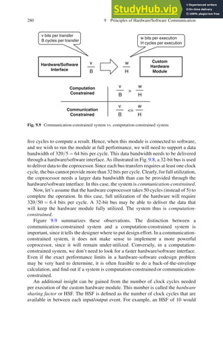
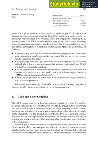


![292 10 On-Chip Busses
1 2 3 4 5
clk
strb_i
strb_o
addr_o[31:0]
data_i[7:0]
vec_i[15:0]
0x8F000000 0x8F000004
0x0
0x12
0xA028 0xF4C0
Fig. 10.4 Bus timing diagram notation
such as cpu1 read data valid sdram0. While such identifiers are tedious
to type, they precisely reflect the function of the wire.
Bus systems may use additional naming conventions to help a designer. For
example, AMBA prefixes all signals on the high-speed bus (AHB) with the letter
H, and all signals on the peripheral bus (APB) with the letter P. Wishbone suffixes
all input pins with the letter I, and all output pins with the letter O. Obviously, for a
designer, it will greatly help to adopt and follow the bus naming conventions of the
particular bus in use: it avoids coding mistakes and connection errors, it makes code
reusable, and it simplifies debugging and verification.
10.1.6 Bus Timing Diagram
Because a bus system reflects a complex, highly parallel entity, timing diagrams
are extensively used to describe the timing relationships of one signal to the other.
Figure 10.4 illustrates a timing diagram of the activities in a generic bus over five
clock cycles. The clock signal is shown on top, and all signals are referenced to the
upgoing clock edge. Dashed vertical lines indicate the timing reference.
Signal buses of several wires can be collapsed into a single trace in the
timing diagram. Examples in Fig. 10.4 are addr o, data i, and vec i. The
label indicates when the bus changes value. For example, addr o changes from
0x8F000000 to 0x00000000 at the third clock edge, and it changes back to
0x8F000004 one clock cycle later. Various schemes exist to indicate that a signal
or a bus has an unknown or don’t care value. The value of data i at the second
clock edge, and the value of vec i at the third clock edge are all unknown.
When discussing timing diagrams, one must make a distinction between clock
edges and clock cycles. The difference between them is subtle, but often causes](https://image.slidesharecdn.com/apracticalintroductiontohardwaresoftwarecodesign-230806184145-7b1ca97e/85/A-Practical-Introduction-To-Hardware-Software-Codesign-307-320.jpg)


![296 10 On-Chip Busses
Table 10.4 Signal naming and numbering for a bus slave input
Signal part Offset CoreConnect/OPB AMBA/APB
Word Sl DBUS[0..31] PWDATA[31..0]
Most significant bit Sl DBUS[0] PWDATA[31]
Little endian byte 0 Sl DBUS[24..31] PWDATA[7..0]
Big endian byte 0 Sl DBUS[0..7] PWDATA[31..24]
Little endian byte 3 Sl DBUS[0..7] PWDATA[31..24]
Big endian byte 3 Sl DBUS[24..31] PWDATA[7..0]
Signal part Offset Avalon-MM Wishbone
Word writedata[31..0] DAT I[31..0]
Most significant bit writedata[31] DAT I[31]
Little endian byte 0 writedata[7..0] DAT I[7..0]
Big endian byte 0 writedata[31..24] DAT I[31..24]
Little endian byte 3 writedata[31..24] DAT I[31..24]
Big endian byte 3 writedata[7..0] DAT I[7..0]
10.2.2 Transfer Sizing and Endianess
By default, all masters and slaves on an on-chip bus will use a uniform wordlength
and a uniform endianess. For example, the masters, the slaves, and the bus could be
using 32-bit little-endian words. This would mean that each data transfer transports
32 bits, and that the least significant byte would be found in the lower byte of the 32-
bit word. As long as the master, the bus, and the slave make identical assumptions on
the data format, a single request and a single acknowledge signal will be adequate
to control the transfer of data.
The numbering of wires within a signal vector depends on the bus. The
documentation of the bus should be consulted to determine the name of the least
significant bit of a word. As an example, Table 10.4 illustrates the signal naming for
a bus slave input under various bus schemes.
While endianess can be configured on most buses, it is a static selection, and
dynamic switching of endianess is not supported by AMBA, Coreconnect, Avalon-
MM or Wishbone. The additional hardware and complexity introduced in the bus
system does not justify the benefit. Indeed, as illustrated in Fig. 10.7, heterogeneous
endianess can be resolved while interconnecting bus components to the bus system.
A bus system will also need to provide a mechanism for transfer sizing: selecting
what part of a given word belongs to the actual data transfer. In a 32-bit data-bus
for example, it is useful to be able to transfer a single byte or a halfword (16 bit).
For example, this would allow a C program to write a single char (8 bit) to memory.
Transfer sizing is expressed using byte-enable signals, or else by directly encoding
the size of the transfer as part of the bus control signals. The former method, using
byte-enable signals, is slightly more general than the latter, because it allows one to
cope with un-aligned transfers.](https://image.slidesharecdn.com/apracticalintroductiontohardwaresoftwarecodesign-230806184145-7b1ca97e/85/A-Practical-Introduction-To-Hardware-Software-Codesign-311-320.jpg)
![10.2 Bus Transfers 297
Bus Master
Bus
Bus Slave
0
7
8
15
16
23
24
31
Fig. 10.7 Connecting a big-endian slave to little-endian master
To see the difference between the two, consider the difference in performance for
a processor running the following C program.
int main() {
unsigned i;
char a[32], *p = a;
for (i=0; i32; i++)
*p++ = (char) (i + 4);
return 0;
}
As the processor moves through all iterations of the i-loop, it will generate byte-
aligned write operations to all addresses occupied by the a array. Assume that this
happens in a system with a 32-bit data bus, and that the third byte of a 32-bit word
needs to be written during a particular iteration. When the bus does not support
unaligned data transfers, the processor will first need to read the word that contains
the byte, update the word by modifying a single byte, and write it back to memory.
On the other hand, when the bus does support unaligned data transfers, the processor
can directly write to the third byte in a word. Therefore, the example program will
complete quicker on systems that support unaligned transfers. Note that unaligned
transfers can also lead to exceptions. For example, processors with a word-level
memory organization do not support transfer of unaligned words. If a programmer
attempts to perform such a transfer, an exception will result, which usually halts the
execution of the program.
Endianess and byte-transfer sizing help bus components to deal with the ordering
of individual bytes within a bus word. In some cases, we may run into the situation
where masters and slaves of different physical width need to be interconnected. For
example, a bus slave could have an 8-bit data bus but needs to be connected to a
32-bit bus. Or, a bus master could have a 64-bit data bus but needs to be connected
to a 32-bit bus. These cases require additional hardware.
Figure 10.8 shows how a 64-bit bus slave and a 16-bit bus slave can be connected
to a 32-bit bus. In the case of the 64-bit bus slave, a data-write will transfer only](https://image.slidesharecdn.com/apracticalintroductiontohardwaresoftwarecodesign-230806184145-7b1ca97e/85/A-Practical-Introduction-To-Hardware-Software-Codesign-312-320.jpg)
![298 10 On-Chip Busses
64-bit Bus Slave
Do[0..63]
Do[0..31]
Addr[2]
1
0
[0..31]
[32..63]
Di[0..31]
0
Di[0..63]
16-bit Bus Slave
Do[0..15] Do[0..31]
Di[0..15]
Addr[1]
0
Di[0..31]
1
0
[0..15]
[16..31]
a
b
Fig. 10.8 (a) Connecting a 64-bit slave to a 32-bit bus. (b) Connecting a 16-bit slave to a 32-bit bus
32 bits at a time; the upper 32 bits are wired to zero. Additionally, the interconnect
may use the byte-enable signals to mask off non-written bytes to the slave.
In the case of a data-read, one of the address lines, Addr[2], will be used to
multiplex the 64 bits of data produced by the bus slave. The net effect of the
multiplexing is that the bus slave appears as a continuous memory region when
data is read.
The case of the 16-bit bus slave is opposite: the 32-bit bus system can deliver
more data than the 16-bit bus slave can handle, and an additional address bit,
Addr[1] is used to determine which part of the 32-bit bus will be transferred to the
16-bit bus slave. If the interconnect supports dynamic transfer sizing, it will expand
each master-side transaction (read or write) into multiple slave-side transactions.
In summary, busses are able to deal with varying wordlength requirements by
the introduction of additional control signals (byte-select signals), and by adding
additional multiplexing hardware around the bus slaves or bus masters. A designer
also needs to be aware of the endianess assumptions made by the on-chip bus, the
bus master, and the bus slave.
10.2.3 Improved Bus Transfers
Each bus data transfer includes multiple phases. First, the bus master has to negotiate
a bus access with the bus arbiter. Next, the bus master has to issue a bus address and
a bus command. Third, the bus slave has to acknowledge the data transfer. Finally,
the bus master has to terminate the bus transfer and release control over the bus.
Each of these activities takes a finite amount of time to complete. Moreover, all of
these activities are sequential, so that the overall system is limited by the speed of
the slowest component. For high-speed buses, this is too slow.](https://image.slidesharecdn.com/apracticalintroductiontohardwaresoftwarecodesign-230806184145-7b1ca97e/85/A-Practical-Introduction-To-Hardware-Software-Codesign-313-320.jpg)


![304 10 On-Chip Busses
Table 10.6 Arbitration signals on CoreConnect/OPB and AMBA/AHB
Signal CoreConnect/PLB AMBA/AHB Avalon-MM
reqx Mx request HBUSREQ Mx transfer request
grantx PLB PAValid HGRANT Mx waitrequest
lock Mx Buslock HLOCK lock
PLB Buslock HMASTLOCK
Mx priority[..]
sel HMASTER[..]
bus, and master 2 will get access to the bus only when master 1 does not need it.
The transfer of master 1 completes at clock edge 6. Since master 2 is still waiting
for access to be granted, it can proceed at clock edge 6 because master 1 no longer
needs to bus. The fourth and final transfer then completes on clock edge 7.
10.3.1 Bus Priority
The timing diagram in Fig. 10.12 reveals the interesting concept of priority. When
multiple masters attempt to access the bus at the same time, only a single master
is allowed to proceed based on priority resolution. The simplest priority scheme is
to allocate a fixed priority, strictly increasing, to every master. While this is easy
to implement, it is not necessarily the best solution. When a high-priority master
continuously accesses the bus, other low-priority masters can be denied bus transfers
for extended amounts of time.
Often, multiple masters on a bus should have equal priority. For example, when
symmetrical multi-processors processors on a single bus access the same memory,
no processor should have priority over the other. In this situation, priority resolution
is implemented using round-robin scheme. Each master takes turns to access to the
bus. When two masters request the bus continuously, then the bus transfers of master
1 and master 2 will be interleaved. Another possible solution is a least-recently-used
scheme, in which the master who was waiting for the bus for the longest time will
get access first. Equal-priority schemes such as round-robin or least-recently-used
avoid starvation of the bus masters, but, they also make the performance of the
bus unpredictable. When working with latency-critical applications, this can be a
problem. To address this, designers can use a mixed scheme that combines multiple
levels of priority with an equal-priority scheme to allow several masters to share the
same priority level.
The priority algorithm used by the bus arbiter is not part of the definition of
the bus transfer protocol. Therefore, Coreconnect/PLB, AMBA/AHB and Avalon-
MM only describe the arbitration connections, but not the priority schemes. The
Wishbone bus is special in that it does not define special bus request/grant signals.
Instead, Wishbone leaves the design of the bus topology to the designer.](https://image.slidesharecdn.com/apracticalintroductiontohardwaresoftwarecodesign-230806184145-7b1ca97e/85/A-Practical-Introduction-To-Hardware-Software-Codesign-319-320.jpg)
![10.3 Multi-master Bus Systems 305
Table 10.6 makes a comparison between the generic bus arbtriation signals
defined above, and those of CoreConnect, AMBA and Avalon. The table also
lists a few arbitration signals that are unique to each individual bus protocol.
The bus locking signals will be explained shortly. The other signals have the
following meaning.
• Mx priority[..] allows a PLB master to select its priority for each transfer.
This scheme allows the master to change its priority level dynamically depending
on the needs of the bus transfer.
• HMASTER[..] is an encoding of the identity of the master that was granted bus
access by the arbiter. The signal is used to drive the bus address multiplexer.
10.3.2 Bus Locking
The final concept in multi-master bus schemes is bus locking: the exclusive
allocation of a bus to a single master for the duration of multiple transfers. There
are several reasons why bus locking may be needed. First, when large blocks of
data need to be transferred with strict latency requirements, exclusive access to the
bus may be required. While burst-mode transfers can help a master to complete
these transfers quickly, these transfers can still be interrupted by another master
with higher priority. By locking the bus, the master can be sure this will not happen.
The second need for bus locking is when a master needs to have guaranteed,
exclusive access to consecutive transfers, typically a read transfer followed by
a write transfer. This is needed, for example when implementing a test-and-set
instruction. The test-and-set instruction is used to create a mutex, a well-known soft-
ware primitive to implement mutual exclusion. A mutex is similar to a semaphore
(discussed in Sect. 9.2.2), but it’s not identical to it. A mutex implies ownership:
once a mutex is locked, it can only be unlocked by the same entity that locked it. An
example where a mutex can be used is to control the access of two bus masters to
a single, shared region of memory. Bus masters will control access using a mutex,
implemented through a test-and-set instruction as discussed next.
An example implementation of test-and-set is shown below. This C program
runs on each of two processors (bus masters) attached to the same bus. They share
a memory location at address 0x8000. By calling testandset, a processor
will try to read this memory location, and write into it during a single locked-bus
operation. This means that the function test and set() cannot be interrupted:
only one processor will be able to read the value of the mutex when its value
is low. The two processors use this function as follows. Before accessing the
shared resource, the processors will call enter(), while they will call leave().
The shared resource can be anything that needs exclusive access by one of the
processors.
int *mutex = (int *) 0x8000; // location of mutex](https://image.slidesharecdn.com/apracticalintroductiontohardwaresoftwarecodesign-230806184145-7b1ca97e/85/A-Practical-Introduction-To-Hardware-Software-Codesign-320-320.jpg)


![312 10 On-Chip Busses
masters and slaves. They use enhancements to improve the performance of on-
chip communication, including pipelining, split-transfers, and burstmode transfers.
On multi-master buses, each transfer needs to be arbitrated. These transfers may
need to be prioritized based on the bus master.
Finally, more recent developments in on-chip communication with System-
on-Chip emphasize distributed solutions in the form of switched busses or
network-on-chip.
The net effect of this evolution is that the design of on-chip communication has
become a design challenge on its own, with many different abstraction layers to
tackle. For the hardware-software codesigner, it’s important to be aware of new
evolutions in this field. The communication latency between hardware and software
remains a fundamental issue that determines if a solution is communication-
constrained and computation-constrained.
10.6 Further Reading
The best reference to study on-chip bus systems is obviously the documentation
from the vendors themselves. The AMBA bus specification can be obtained
online from ARM (2009a). Likewise, the CoreConnect bus specification can be
obtained online from IBM (2009), and the Avalon specification is available from
Altera (2011). An in-depth discussion of contemporary on-chip bus systems,
including AMBA and CoreConnect, is available from Pasricha and Dutt (2008).
The same book also reviews ongoing research topics for on-chip bus systems.
Recently research efforts have focused on network-on-chip. An overview of the
design principles may be found in De Micheli’s book (Micheli and Benini 2006).
A recent special issue of IEEE Design and Test Magazine has reviewed several
proposals and open research issues (Ivanov and De Micheli 2005).
10.7 Problems
Problem 10.1. The timing diagram in Fig. 10.17 illustrates a write operation on
the AMBA peripheral bus, AMBA APB. A memory-mapped register is a register
which is able to intercept bus transfers from a specific address. In this case, we
wish to create logic which will write PWDATA into a register when a write to
address 0x2000 occurs. Develop a logic expression for the logic module shown
in Fig. 10.17. Assume a 16-bit address.
Listing 10.1 Program for Problem 10.2
#include stdio.h
void main() {
int i, a[0x40];](https://image.slidesharecdn.com/apracticalintroductiontohardwaresoftwarecodesign-230806184145-7b1ca97e/85/A-Practical-Introduction-To-Hardware-Software-Codesign-327-320.jpg)
![10.7 Problems 313
1 2 3 4 5
clk
PADDR
PWRITE
PENABLE
PWDATA
PSEL
0x2000
data
PWDATA
PADDR
PWRITE
PENABLE
PSEL
Logic
Fig. 10.17 Timing diagram and schematic for Problem 10.1
Fig. 10.18 Timing diagram for Problem 10.2
for (i=0; i 0x40; i++)
if (i 0x23)
a[i] = a[i-1] + 1;
else
a[i] = 0x5;
}
Problem 10.2. While debugging a C program on a 32-bit microprocessor (shown in
Listing 10.1), you capture the bus transfer shown in Fig. 10.18. The microprocessor
is attached to an off-chip memory that holds the program and the data. The
text and data segment both are stored in an off-chip memory starting at address
0x44000000. The array a[] starts at address 0x44001084. The instructions
from the body of the loop start at address 0x44000170. Observe closely the timing
diagram in Fig. 10.18 and answer the questions below.](https://image.slidesharecdn.com/apracticalintroductiontohardwaresoftwarecodesign-230806184145-7b1ca97e/85/A-Practical-Introduction-To-Hardware-Software-Codesign-328-320.jpg)
![314 10 On-Chip Busses
Table 10.7 List of bus
transactions for Problem 10.3
Transaction m addr m data m rnw
0 0x3F68 1 0
1 0x3F78 1 0
2 0x3F68 2 0
3 0x3F74 2 0
4 0x3F68 3 0
5 0x3F70 3 0
6 0x3F68 4 0
7 0x3F68 5 0
8 0x3F68 6 0
(a) The cursor X in Fig. 10.18 is positioned at a point for which the address bus
contains 0x4400111C and the data bus contains 0x8. Is this a memory read of a
memory write?
(b) For the same cursor position ‘X’, is this memory access for an instruction-fetch
or for a data-memory read?
(c) For the same cursor position ‘X’, what is the value of the loop counter i from
the C program?
Listing 10.2 Program for Problem 10.3
int main() {
int i, a[32];
for (i=1; i32; i++)
if (i4)
a[4-i] = i;
return 0;
}
Problem 10.3. You are debugging an embedded system by recording bus trans-
actions between a microprocessor and an on-chip memory. The program you’re
analyzing is shown in Listing 10.2. Table 10.7 lists a sequence of bus transactions
you observe when m rnw is low. The signals in the Table follow the naming
convention of the generic bus (defined in Table 10.2). Analyze the transactions and
answer the questions below.
(a) What is the memory address of variable i?
(b) What is the memory address of variable a[0]?
Problem 10.4. The timing diagram in Fig. 10.19 shows the arbitration process of
two masters, M1 and M2, requesting access to a shared bus. Answer the questions
below using the information provided in the timing diagram.
(a) Based on the timing diagram, which master has the highest priority for bus
transfers: M1, M2 or impossible to tell?
(b) Which master has control over the address bus between clock edge 3 and clock
edge 4: M1, M2, or impossible to tell?](https://image.slidesharecdn.com/apracticalintroductiontohardwaresoftwarecodesign-230806184145-7b1ca97e/85/A-Practical-Introduction-To-Hardware-Software-Codesign-329-320.jpg)

![316 10 On-Chip Busses
PLB bus transfer. The cursors indicate data memory accesses to variables in the
C program.
(a) What memory operation is performed under the X cursor: read or write?
(b) What variable from the C program is accessed under the O cursor ?
(c) What is the base address of the array a?
Listing 10.3 Program for Problem 10.5
int main () {
int i, a[32];
for (i = 1; i 32; i++)
if (i 8)
a[i+1] = i;
return 0;
}](https://image.slidesharecdn.com/apracticalintroductiontohardwaresoftwarecodesign-230806184145-7b1ca97e/85/A-Practical-Introduction-To-Hardware-Software-Codesign-331-320.jpg)


![11.1 Memory-Mapped Interfaces 327
82 @s0 (ack0, wait) - s1;
83
84 // read m
85 @s1 if (r_req) then (getm, ack1, wait) - s2;
86 else (ack0, wait) - s1;
87 // read n
88 @s2 if (˜r_req) then (getn, ack0, wait) - s3;
89 else (ack1, wait) - s2;
90
91 // compute
92 @s3 (start, ack0) - s4;
93 @s4 if (r_done) then (ack0, wait) - s5;
94 else (ack0, wait) - s4;
95
96 // output result
97 @s5 if (r_req) then (ack1, wait) - s6;
98 else (ack0, wait) - s5;
99 @s6 if (˜r_req) then (ack0, wait) - s1;
100 else (ack1, wait) - s6;
101 }
102
103 system S {
104 tb_euclid;
105 }
Listing 11.2 shows a C driver program that matches the coprocessor design of
Listing 11.1. The program evaluates the GCD operation of the numbers 80 and 12,
followed by the GCD of the numbers 80 and 13. Note the difference between a
master handshake protocol, as shown in the functions sync1() and sync0(),
and a slave handshake protocol, as illustrated in the FSM transitions in Listing 11.1.
In a master handshake, the request signals are written first, and followed by reading
and testing of the acknowledge signals. In a slave handshake, the request signals are
tested first, followed by a response on the acknowledge signals.
Executing this cosimulation is easy. We first cross-compile the C program to
an executable. Next, we run the cosimulator on the executable and the GEZEL
program.
arm-linux-gcc -static gcddrive.c -o gcddrive
gplatform gcd.fdl
core my_arm
armsystem: loading executable [gcddrive]
armsystemsink: set address 2147483652
armsystemsink: set address 2147483660
gcd(80,12) = 4
gcd(80,13) = 1
Total Cycles: 11814
In conclusion, memory-mapped interfaces are a general-purpose mechanism
to create hardware/software interfaces. The principle of a two-way handshake
is applicable to many different situations. In this case, hardware and software
are synchronized using simple shared storage locations. Because memory-mapped
interfaces rely on a general-purpose on-chip bus, they easily become a bottleneck](https://image.slidesharecdn.com/apracticalintroductiontohardwaresoftwarecodesign-230806184145-7b1ca97e/85/A-Practical-Introduction-To-Hardware-Software-Codesign-342-320.jpg)


![11.2 Coprocessor Interfaces 333
Instruction
Fetch
Coprocessor
Interface
Microprocessor
Floating-Point
Coprocessor
operands[2*64]
opcode[9]
opid[6]
flush
flushid[6]
result[64]
resid[6]
allow[3]
except[6]
FP
Registers
Integer
Pipeline
Linear
Pipeline
(Add,
Sub,
Mul)
Non
Linear
Pipeline
(Div,
Sqrt)
Fig. 11.10 GRFPU floating point coprocessor interface
Linear Pipeline
Non-Linear Pipeline
1
1
1
3
3
3
4
4
4
6
6
6
2
2 2 2 2
2
5
5 5 5 5
5
Operands
Instruction Issue
Results
1 3 4 6
2 5
1 3 4 6
2 5
stage 2
stage 3
stage 1
stage 2
stage 3
stage 1
cycles
Fig. 11.11 GRFPU instruction issue and result return
be merged in the microprocessor in the same order as their operands are dispatched
to the FPU. Figure 11.11 demonstrates that, due to the complex pipeline architecture
of the FPU however, results may arrive out-of-order. The GRFPU interface handles
this problem.
• Each operation for the FPU is provided as a set of operands, with a given
opcode, and an instruction identifier opid. When the FPU operation finishes, it
returns the result, together with a corresponding instruction identifier resid.
By examining the value of resid, the processor can determine what result](https://image.slidesharecdn.com/apracticalintroductiontohardwaresoftwarecodesign-230806184145-7b1ca97e/85/A-Practical-Introduction-To-Hardware-Software-Codesign-348-320.jpg)


![336 11 Microprocessor Interfaces
Compared to SoC design based on custom-hardware modules, will the ASIP
design flow in Fig. 11.12 always deliver better performance? Not in the general
case. Keep in mind that the basic architecture template of an ASIP is a sequential
processor. The fundamental bottlenecks of the sequential processor (memory-
access, sequential execution of code) are also fundamental bottlenecks for an ASIP
design.
Compared to SoC design based on custom-hardware modules, can the ASIP
design flow deliver less error-prone results? Yes, it can for the following two
reasons. First, the design process is incremental. A functional error can be detected
very quickly, in the early phases of the design. Second, it works at a higher level of
abstraction. The application is modeled in C. The processor description language is
also at a higher level of abstraction, compared to hardware description languages.
In the past few years, a tremendous progress has been made on design tools that
support the ASIP design flow. All of the shaded boxes in Fig. 11.12 can be obtained
as commercial tools.
11.3.2 Example: Endianness Byte-Ordering Processor
We describe an example of ASIP design, as well as GEZEL modeling of the custom-
instruction. The application is an endianness byte-ordering processor.
Figure 11.13 illustrates the design problem. Processors have a chosen byte-
ordering or endianness. When a processor transmits data words over a network, the
byte order of the transmitted packets is converted from the processor byte-order into
network byte-order, which is big-endian in practice. For example, when a processor
is little endian, it will store the word 0x12345678 with the lowest significant
byte in the lowest memory address. However, when that word is transmitted over a
network, the packet byte-order must follow a big-endian convention that will send
0x78 first and 0x12 last. The communication protocol stack on the processor will
therefore convert each word from little-endian format to big-endian format before
handing it off to the network buffer on the Ethernet card.
For a 32-bit processor, endianness conversion involves byte-level manipulation
using shifting and masking. The following is an example of a function that converts
little-endian to big-endian (or vice versa) in C.
for (i=0; i4096; i++)
ot[i] = ( ((in[i] 0x000000ff) 24) |
((in[i] 0x0000ff00) 8) |
((in[i] 0x00ff0000) 8) |
((in[i] 0xff000000) 24));
On a StrongARM processor (which is little-endian), this loop requires 13 cycles
per iteration (assuming no cache misses). Examining the assembly, we would find
that there are 11 instructions inside of the loop, leaving two cycles of pipeline stalls
per iteration – one for the branch and one data-dependency (ldr instruction).](https://image.slidesharecdn.com/apracticalintroductiontohardwaresoftwarecodesign-230806184145-7b1ca97e/85/A-Practical-Introduction-To-Hardware-Software-Codesign-351-320.jpg)
![11.3 Custom-Instruction Interfaces 337
strongARM
little endian
network
(big endian)
powerPC
big endian
0x12
0x34
0x56
0x78
0x1234:5678
0x34
0x56
0x78
0x12
0x1234:5678
0x78
0x56
0x34
0x12
Fig. 11.13 Endianness byte-ordering problem
.L6:
ldr r3, [r4, ip, asl #2] ; read in[i]
and r2, r3, #65280 ; evaluate ot[i]
mov r2, r2, asl #8 ; ...
orr r2, r2, r3, asl #24 ; ...
and r1, r3, #16711680 ; ...
orr r2, r2, r1, lsr #8 ; ...
orr r2, r2, r3, lsr #24 ; ...
str r2, [r0, ip, asl #2] ; and write back
add ip, ip, #1 ; next iteration
cmp ip, lr ;
ble .L6
Let’s consider possible design improvements. In hardware, the endianness-
conversion is obviously very simple: it is a simple wiring pattern. The hardware-
software codesign problem, therefore, essentially revolves around the problem of
moving data around. Before designing an ASIP, let’s try to solve this problem with
a memory-mapped coprocessor.
The memory-mapped coprocessor looks as follows. It uses two memory-mapped
registers, one for input and one for output.
ipblock myarm {
iptype armsystem;
ipparm exec=byteswap;
}
ipblock port1(out data : ns(32)) {
iptype armsystemsource;
ipparm core=myarm;
ipparm address = 0x80000000;
}
ipblock port2(in data : ns(32)) {](https://image.slidesharecdn.com/apracticalintroductiontohardwaresoftwarecodesign-230806184145-7b1ca97e/85/A-Practical-Introduction-To-Hardware-Software-Codesign-352-320.jpg)
![338 11 Microprocessor Interfaces
iptype armsystemsink;
ipparm core=myarm;
ipparm address = 0x80000004;
}
dp mmswap(in d1 : ns(32); out q1 : ns(32)) {
always {
q1 = d1[ 7: 0] #
d1[15: 8] #
d1[23:16] #
d1[31:24];
}
}
dp top {
sig d, q : ns(32);
use myarm;
use port1(d);
use port2(q);
use mmswap(d, q);
}
system S {
top;
}
The C driver program for this memory-mapped coprocessor looks as follows.
volatile unsigned int * mmin = (unsigned int *) 0x80000000;
volatile unsigned int * mmot = (unsigned int *) 0x80000004;
for (i=0; i4096; i++) {
*mmin = in[i];
ot[i] = *mmot;
}
The equivalent StrongARM assembly program for this loop looks as follows.
.L21:
ldr r3, [r0, ip, asl #2] ; load in[i]
str r3, [r4, #0] ; send to coprocessor
ldr r2, [r5, #0] ; read from coprocessor
str r2, [r1, ip, asl #2] ; write ot[i]
add ip, ip, #1 ; next iteration
cmp ip, lr
ble .L21
The execution time of the loop body now takes ten clock cycles per iteration
(seven instructions, one stall for branching, two stall for data-dependencies). This is
a gain of three cycles. We assume that we have single-cycle access to the memory-
mapped coprocessor, which is hard to achieve in practice. Hence, the gain of three
cycles will probably be lost in a real design. The problem with this design is apparent
from the assembly program: each data element travels four times over the memory
bus in order to be converted.](https://image.slidesharecdn.com/apracticalintroductiontohardwaresoftwarecodesign-230806184145-7b1ca97e/85/A-Practical-Introduction-To-Hardware-Software-Codesign-353-320.jpg)
![11.3 Custom-Instruction Interfaces 339
Instruction
Memory Read
Instruction
Fetch
Instruction
Decode
Instruction
Decode
Register
Read
Execute Datapath
Operation
Evaluate
Next-PC
Buffer Data
Memory R/W
Write-back Register
Write
Custom Datapath
Fig. 11.14 Single-argument custom-datapath in an ASIP
Using an ASIP, this wasteful copying over the memory bus can be avoided: we
can retrieve in[i] once, convert it inside of the processor, and write back the
converted result to ot[i]. In order to do this as part of an instruction, we need to
modify (extend) the datapath of the processor with a new operation. Figure 11.14
illustrates how this works: the execution stage of the pipeline is extended with a
new datapath (endianness conversion), and a new instruction is integrated into the
instruction decoder.
GEZEL supports experiments with custom datapaths in a StrongARM processor,
by using several unused opcodes of that processor. In particular, GEZEL supports 2-
by-2 and 3-by-1 custom datapaths in a StrongARM. A 2-by-2 custom datapath reads
two register operands and produces two register operands. A 3-by-1 custom datapath
reads three register operands and produces a single register operand. The following
GEZEL program shows a 2-by-2 custom datapath for endianness conversion. An
ipblock of type armsfu2x2 is used to represent a custom instruction.
ipblock myarm {
iptype armsystem;
ipparm exec=nettohost_sfu;
}
ipblock armsfu(out d1, d2 : ns(32);
in q1, q2 : ns(32)) {
iptype armsfu2x2;
ipparm core = myarm;
ipparm device=0;
}](https://image.slidesharecdn.com/apracticalintroductiontohardwaresoftwarecodesign-230806184145-7b1ca97e/85/A-Practical-Introduction-To-Hardware-Software-Codesign-354-320.jpg)
![340 11 Microprocessor Interfaces
dp swap(in d1, d2 : ns(32);
out q1, q2 : ns(32)) {
always {
q1 = d1[ 7: 0] #
d1[15: 8] #
d1[23:16] #
d1[31:24];
q2 = d2[ 7: 0] #
d2[15: 8] #
d2[23:16] #
d2[31:24];
}
}
dp top {
sig d1, d2, q1, q2: ns(32);
use armsfu(d1, d2, q1, q2);
use swap (d1, d2, q1, q2);
use myarm;
}
We will now write a C program to use this custom datapath. We need to
make use of a custom opcode to trigger execution of the custom datapath. The
GEZEL armsfu interface relies on the smullnv opcode, which is unused by
the C compiler (arm-linux-gcc 3.2). Since smullnv cannot be written
directly in C, its opcode is inserted in a regular program by making use of inline
assembly. The following C snippet shows how to define an inline assembly macro,
and how to call this instruction for a single-argument and a double-argument
instruction.
#define OP2x2_1(D1, D2, S1, S2)
asm volatile (smullnv %0, %1, %2, %3 :
=r(D1), =r(D2) :
r(S1), r(S2));
// use as a single-argument instruction
for (i=0; i4096; i++) {
OP2x2_1(ot[i], dummy1, in[i], dummy2);
}
// use as a dual-argument instruction
for (i=0; i2048; i++) {
OP2x2_1(ot[2*i], ot[2*i+1], in[2*i], in[2*i+1]);
}
The resulting assembly for the single-argument case now looks as follows. The
loop requires eight cycles, used by six instructions and two stalls. This is a gain
of two clock cycles compared to the previous case. Equally important is that the
program now only needs half the bus transfers, since the coprocessor is integrated
inside of the StrongARM.](https://image.slidesharecdn.com/apracticalintroductiontohardwaresoftwarecodesign-230806184145-7b1ca97e/85/A-Practical-Introduction-To-Hardware-Software-Codesign-355-320.jpg)
![11.3 Custom-Instruction Interfaces 341
Table 11.1 Performance summary for the endianness byte-ordering processor
Type Software Memory-mapped ASIP (1x1) ASIP (2x2)
Instructions 11 7 6 7
Pipeline stalls 2 3 2 2
Cycles/iteration 13 10 8 9
Cycles/word 13 10 8 4.5
.L38:
ldr r3, [r4, lr, asl #2] ; load in[i]
smullnv r2, r7, r3, ip ; perform conversion
str r2, [r1, lr, asl #2] ; write ot[i]
add lr, lr, #1 ; next iteration
cmp lr, r0
ble .L38
The dual-argument design is even more efficient, because the loop management
code is now shared over two endianness conversions. We have nine cycles per
loop iteration: seven instructions and two stalls. However, each iteration of the
loop performs two conversions, so that the effective cycle cost is 4.5 cycles per
endianness conversion (compared to eight cycles in the previous case).
.L53:
ldr r1, [r5], #4 ; read in[2*i], adjust pointer
ldr r2, [r5], #4 ; read in[2*i+1], adjust pointer
smullnv r0, ip, r1, r2 ; perform conversion
str r0, [r4], #4 ; store ot[2*i], adjust pointer
subs lr, lr, #1 ; next iteration
str ip, [r4], #4 ; store ot[2*i+1], adjust pointer
bne .L53
Summing up, by converting an all-software design to an ASIP-type design, the
cycle cost for endianness conversion on a StrongARM reduces from 13 cycles per
word to 4.5 cycles per word, an improvement of 2.9 times. Table 11.1 summarizes
the performance of different configurations.
What is the limiting factor of the final design (ASIP 2x2)? Based on the
code listing, 4 of the 7 instructions are load and store instructions. In other words,
the majority of the execution time is spent in moving data between memory and the
processor. This illustrates a point we made earlier: the strength of an ASIP design is
also its weakness. An instruction-set architecture is convenient to build extensions,
but bottlenecks in the instruction-set architecture will also be bottlenecks in the
resulting hardware/software codesign.
11.3.3 Example: The Nios-II Custom-Instruction Interface
The Nios-II processor has an custom-instruction interface to attach hardware
modules. Following our earlier definition of ASIP vs. coprocessor interface, we](https://image.slidesharecdn.com/apracticalintroductiontohardwaresoftwarecodesign-230806184145-7b1ca97e/85/A-Practical-Introduction-To-Hardware-Software-Codesign-356-320.jpg)


![11.3 Custom-Instruction Interfaces 345
• The number of input and output operands must be limited to ensure that
the register-file bandwidth stays within bounds. Indeed, as the new custom
instruction executes, it will require all the input arguments to be available at
the same clock cycle, and it will produce all output arguments at the same clock
cycle.
• The length of the chained operations must not be too long, since this adversely
affects the critical path of the processor.
Figure 11.17b shows an example of operator compounding. In this case, we
are combining multiple possibly unrelated operations together, especially when
they share common inputs. The operator compounds are identified using data-flow
analysis of the assembly code, and they have similar limitations as fused operators.
We’ll now consider the endianness-conversion example once more and consider
how much more it can be optimized beyond a single OP2x2 ASIP instruction for
endianness conversion. In this case, we consider a complete C function as follows.
Notice how this code has been optimized with incremental pointer arithmetic.
void byteswap(unsigned *in, unsigned *ot) {
int i;
int d1, d2, d3, d4;
unsigned *q1 = in;
unsigned *q2 = ot;
for (i=0; i2048; i++) {
d1 = *(q1++);
d2 = *(q1++);
OP2x2_1(d3, d4, d1, d2);
*(q2++) = d3;
*(q2++) = d4;
}
}
The assembly code for this function looks as follows. The loop body contains
nine instructions. Only a single instruction performs the actual byte swap operation!
Four other instructions are related to moving data into and out of the processor (ldr,
str), two instructions do loop counter management (cmp, add), one instruction
implements a conditional return (ldmgtfd) and one instruction is a branch. There
will be two pipeline stalls: one for the branch, and one for the second memory-load
(ldr).
byteswap:
stmfd sp!, {r4, r5, lr} ; preserve registers
mov ip, #0 ; init loop counter
mov lr, #2032 ; loop counter limit
add lr, lr, #15
.L76:
ldr r2, [r0], #4 ; load in[i]
ldr r3, [r0], #4 ; load in[i+1]
smullnv r4, r5, r2, r3 ; endianness conversion
str r4, [r1], #4 ; store ot[i]
str r5, [r1], #4 ; store ot[i+1]
add ip, ip, #1 ; increment loop counter](https://image.slidesharecdn.com/apracticalintroductiontohardwaresoftwarecodesign-230806184145-7b1ca97e/85/A-Practical-Introduction-To-Hardware-Software-Codesign-360-320.jpg)

![11.4 Summary 347
fusion candidates. However, we may still reduce the footprint of the loop body
by collapsing the store and load instructions in store-multiple and load-multiple
instructions.
The resulting assembly code after these transformations would therefore look as
follows. The loop body contains six instructions, but will have three stalls (one for
ldm, one for the data dependency from ldm to smullnv, and one for the branch).
A loop round-trip now costs 9 cycles, or 4.5 cycles per word. This is as fast as we
found before, but in this version of the code, function call overhead is included.
byteswap:
stmfd sp!, {r4, r5, lr} ; preserve registers
initloop ip, lr, #0, #2047 ; loop-counter instruction 1
.L76:
ldm r0!, {r2, r3} ; load in[i], in[i+1]
smullnv r4, r5, r2, r3 ; endianness conversion
stm r1!, {r4, r5} ; store ot[i], ot[i+1]
incloop ip, lr ; loop counter instruction 2
ldmgtfd sp!, {r4, r5, pc} ; and conditionally return
b .L76
This concludes our discussion of the third type of hardware/software interface,
the custom instruction. The design of customized processors is an important
research topic, and optimizations have been investigated far beyond the examples we
discussed above. For the hardware/software codesigner, it’s important to understand
that ASIP design takes a top-down view on the codesign problem: one starts
with a C program, and next investigates how to improve its performance. In a
classic coprocessor design, the view is bottom-up: one starts with a given kernel
in hardware, and next investigates how to integrate it efficiently into a system. Both
approaches are viable, and in both cases, a codesigner has to think about interfacing
hardware and software efficiently.
11.4 Summary
Microprocessor interfaces are at the core of hardware/software codesign. We made
a distinction between three classes of interfaces, each with a different integration
within the System on Chip architecture.
A memory-mapped interface reuses the addressing mechanism of an on-chip bus
to reserve a few slots in the address space for hardware/software communication.
Single memory locations can be implemented using memory-mapped registers. A
range of memory locations can be implemented using a shared-memory. Specialized
communication mechanisms, such as FIFO queues, further improve the characteris-
tics of the hardware/software communication channel.
The coprocessor interface is a second type of hardware/software interface. It
requires a dedicated port on a microprocessor, as well as a few predefined instruc-
tions to move data through that port. We discussed two examples of this interface,](https://image.slidesharecdn.com/apracticalintroductiontohardwaresoftwarecodesign-230806184145-7b1ca97e/85/A-Practical-Introduction-To-Hardware-Software-Codesign-362-320.jpg)


![350 11 Microprocessor Interfaces
Listing 11.3 C program for Problem 11.5
int findmax(unsigned int data[1024]) {
unsigned int max = 0;
int i;
for (i=0; i1024; i++)
if (max data[i])
max = data[i];
return max;
}
Listing 11.4 Assembly program for Problem 11.5
findmax:
mov r2, #0
mov r1, #1020
mov ip, r2
add r1, r1, #3
.L7:
ldr r3, [r0, r2, asl #2]
cmp ip, r3
strcc ip, [r0, r2, asl #2]
add r2, r2, #1
cmp r2, r1
movgt r0, #0
movgt pc, lr
b .L7
Listing 11.5 C program for Problem 11.6
int absmax(int v, int w) {
return (v * 6 + w * 4);
}
(c) Design a GEZEL datapath for this custom instruction, following the example in
Sect. 11.3.2.
Problem 11.6. The C function of Listing 11.5 was compiled to a Microblaze
processor and results in the assembly code of Listing 11.6. The input arguments of
the assembly code are r5 and r6; the return argument is r3; the return instruction
was left out of the assembly.
(a) Perform dataflow analysis on the assembly code and draw the data dependency
diagram below. Use rectangles to indicate registers and circles to indicate
operations. Label the operations ‘op1’ to ‘op6’.
(b) When you have drawn the dataflow dependency diagram, define several ASIP
candidate instructions (at least 2) using operation fusion. Indicate clearly which
operations you could merge into ASIP instructions.](https://image.slidesharecdn.com/apracticalintroductiontohardwaresoftwarecodesign-230806184145-7b1ca97e/85/A-Practical-Introduction-To-Hardware-Software-Codesign-365-320.jpg)
![11.6 Problems 351
Listing 11.6 Assembly program for Problem 11.6
// input arg: r5, r6
// return arg: r3
addk r3,r5,r5 // op1
addk r3,r3,r5 // op2
addk r3,r3,r3 // op3
addk r6,r6,r6 // op4
addk r6,r6,r6 // op5
addk r3,r3,r6 // op6
HW
co-
processor
on-chip
instruction
memory
on-chip
data
memory
CPU
int a[1000], r[1000];
void transform() {
int i;
int *ra = a;
int *rr = r;
for (i=0; i1000; i++)
*rr++ = call_coproc(*ra++);
}
on-chip bus
3 cycles
per access
5 cycles
per call
Fig. 11.20 Architecture and C program for Problem 11.7
Problem 11.7. The system-on-chip in Fig. 11.20 combines a coprocessor, a pro-
cessor, and on-chip data- and instruction-memory. The processor will copy each
element of an array a[] to the coprocessor, each time storing the result as an
element of an array r[]. The C program that achieves this is shown on the right
of Fig. 11.20. All the operations in this architecture take zero time to execute, apart
from the following two: accessing the on-chip data memory takes three cycles, and
processing a data item on the coprocessor takes five cycles.
(a) Find the resulting execution time of the C program.
(b) Show how you can rewrite the C program so that the resulting execution time
becomes smaller than 8,000 cycles. As a hint, assume that you can rewrite
the y = call coproc(x); function call as two separate calls. The first
call is send coproc(x);, and it issues an argument from software to the
coprocessor. The second call is y = get coproc();, and it takes a result
from the coprocessor.
Problem 11.8. An ASIP processor performs operations on a stream of samples.
The samples appear at fixed rate. The samples are processed using an algorithm A.
Which of the following optimizations will reduce the energy consumption E needed
to process a single sample? The answer for each question is one of: yes, no,
impossible to decide.](https://image.slidesharecdn.com/apracticalintroductiontohardwaresoftwarecodesign-230806184145-7b1ca97e/85/A-Practical-Introduction-To-Hardware-Software-Codesign-366-320.jpg)


![13.1 The Trivium Stream Cipher Algorithm 377
Stream
Cipher
Kernel
keystream
Stream
Cipher
Kernel
Stream
Cipher
Kernel
Stream
Cipher
Kernel
key key key
key
n n n n
4.n
Fig. 13.2 Parallel stream cipher implementation
Listing 13.1 Trivium round
state s[1..288];
loop
t1 = s[66] + s[93];
t2 = s[162] + s[177];
t3 = s[243] + s[288];
z = t1 + t2 + t3;
t1 = t1 + s[91].s[92] + s[171];
t2 = t2 + s[175].s[176] + s[264];
t3 = t3 + s[286].s[287] + s[69];
s[1..93] = t3 || s[1..s92];
s[94..177] = t1 || s[94..176];
s[178..288] = t2 || s[178..287];
end loop
13.1.2 Trivium
Trivium is a stream cipher with a state register of 288 bits. The state register
is initialized based on an 80-bit key and an 80-bit initial value (IV). After ini-
tialization, Trivium produces a stream of keybits. The specification of Trivium
keystream generation is shown in Listing 13.1. Each iteration of the loop, a single
output bit z is generated, and the state register s is updated. The addition and
multiplication (+ and .) are taken over GF(2). They can be implemented with
exclusive-or and bitwise-and respectively. The double-bar operation (||) denotes
concatenation.
The initialization of the state register proceeds as follows. The 80-bit key K and
the 80-bit initial value IV are loaded into the state register, and the state register is
updated 1,152 times (4 times 288) without producing keybits. After that, the state
register is ready to produce keystream bits. This is illustrated in the pseudocode of
Listing 13.2.](https://image.slidesharecdn.com/apracticalintroductiontohardwaresoftwarecodesign-230806184145-7b1ca97e/85/A-Practical-Introduction-To-Hardware-Software-Codesign-391-320.jpg)
![378 13 Trivium Crypto-Coprocessor
Listing 13.2 Trivium initialization
state s[1..287];
s[1..s92] = K || 0;
s[94..177] = IV || 0;
s[178 .. 288] = 3;
loop for (4 * 288)
t1 = s[66] + s[93] + s[91].s[92] + s[171];
t2 = s[162] + s[177] + s[175].s[176] + s[264];
t3 = s[243] + s[288] + s[286].s[287] + s[69];
s[1..93] = t3 || s[1..s92];
s[94..177] = t1 || s[94..176];
s[178..288] = t2 || s[178..287];
end loop
These listings confirm that, from a computational perspective, Trivium is a
very simple algorithm. A single state register update requires nine single-bit xor
operations and three single-bit and operations. We need two additional single-bit
xor operations to produce the output bit z.
13.1.3 Hardware Mapping of Trivium
A straightforward hardware mapping of the Trivium algorithm requires 288 regis-
ters, 11 xor gates, and 3 and gates. Clearly, the largest cost of this algorithm is in the
storage. Figure 13.3 shows how Trivium is partitioned into hardware modules.
• The trivium module calculates the next state. We will use the term Trivium
kernel to indicate the loop body of Listing 13.1, without the state register update.
• The keyschedule module manages state register initialization and update.
The keyschedule module has a single control input ld to control state
register initialization. In addition, keyschedule has a single status bit e
that indicates when the initialization has completed, and thus when the output
keystream z is valid. This partitioning between keyschedule and trivium kernel
was done with loop unrolling in mind (Fig. 13.2).
Based on this partitioning and the Trivium specification given earlier, it is
straightforward to create a GEZEL description of Trivium. Listing 13.3 shows
the implementation of a 1 bit per cycle Trivium. The control signals in the
keyschedule module are created based on a counter which is initialized after
a pulse on the ld control input.
To create a bit-parallel keystream, we need to modify the code as follows. First,
we need to instantiate the trivium module multiple times, and chain the state
input and output ports together as shown in Fig. 13.2. Second, we need to adjust
the key schedule, since the initialization phase will take less than 4 times 288 clock
cycles. As an example, Listing 13.4 shows how to unroll Trivium eight times, thus](https://image.slidesharecdn.com/apracticalintroductiontohardwaresoftwarecodesign-230806184145-7b1ca97e/85/A-Practical-Introduction-To-Hardware-Software-Codesign-392-320.jpg)
![13.1 The Trivium Stream Cipher Algorithm 379
Listing 13.3 1-bit-per-cycle Trivium
1 dp trivium(in si : ns(288); // state input
2 out so : ns(288); // state output
3 out z : ns(1)) { // crypto bit out
4 sig t1, t2, t3 : ns( 1);
5 sig t11, t22, t33 : ns( 1);
6 sig saa : ns( 93);
7 sig sbb : ns( 84);
8 sig scc : ns(111);
9 always {
10 t1 = si[ 65] ˆ si[ 92];
11 t2 = si[161] ˆ si[176];
12 t3 = si[242] ˆ si[287];
13 z = t1 ˆ t2 ˆ t3;
14 t11 = t1 ˆ (si[ 90] si[ 91]) ˆ si[170];
15 t22 = t2 ˆ (si[174] si[175]) ˆ si[263];
16 t33 = t3 ˆ (si[285] si[286]) ˆ si[ 68];
17 saa = si[ 0: 92] # t33;
18 sbb = si[ 93:176] # t11;
19 scc = si[177:287] # t22;
20 so = scc # sbb # saa;
21 }
22 }
23
24 dp keyschedule(in ld : ns(1); // reload key iv
25 in iv : ns(80); // initialization vector
26 in key : ns(80); // key
27 out e : ns(1); // output valid
28 in si : ns(288); // state input
29 out so : ns(288)) { // state output
30 reg s : ns(288); // state register
31 reg cnt : ns(11); // initialization counter
32 sig saa : ns( 93);
33 sig sbb : ns( 84);
34 sig scc : ns(111);
35 sig cte : ns(111);
36 always {
37 saa = ld ? key : si[ 0: 92];
38 sbb = ld ? iv : si[ 93:176];
39 cte = 7;
40 scc = ld ? (cte 108) : si[177:287];
41 s = scc # sbb # saa;
42 so = s;
43 cnt = ld ? 1152 : (cnt ? cnt - 1 : cnt); 1152 = 4 * 288
44 e = (cnt ? 0 : 1);
45 }
46 }](https://image.slidesharecdn.com/apracticalintroductiontohardwaresoftwarecodesign-230806184145-7b1ca97e/85/A-Practical-Introduction-To-Hardware-Software-Codesign-393-320.jpg)

![13.1 The Trivium Stream Cipher Algorithm 381
8 dp trivium4 : trivium
9 dp trivium5 : trivium
10 dp trivium6 : trivium
11 dp trivium7 : trivium
12 dp trivium8 : trivium
13
14 dp keyschedule(in ld : ns(1); // reload key iv
15 in iv : ns(80); // initialization vector
16 in key : ns(80); // key
17 out e : ns(1); // output valid
18 in si : ns(288); // state input
19 out so : ns(288)) { // state output
20 reg s : ns(288); // state register
21 reg cnt : ns(11); // initialization counter
22 sig saa : ns( 93);
23 sig sbb : ns( 84);
24 sig scc : ns(111);
25 sig cte : ns(111);
26 always {
27 saa = ld ? key : si[ 0: 92];
28 sbb = ld ? iv : si[ 93:176];
29 cte = 7;
30 scc = ld ? (cte 108) : si[177:287];
31 s = scc # sbb # saa;
32 so = s;
33 cnt = ld ? 143 : (cnt ? cnt - 1 : cnt); 143 = 4 * 288 / 8 - 1
34 e = (cnt ? 0 : 1);
35 }
36 }
37
38 dp triviumtop(in ld : ns(1); // reload key iv
39 in iv : ns(80); // initialization vector
40 in key : ns(80); // key
41 out z : ns(8); // encrypted output
42 out e : ns(1)) { // output valid
43 sig si, so0, so1, so2, so3, so4, so5, so6, so7 : ns(288);
44 sig z0, z1, z2, z3, z4, z5, z6, z7 : ns(1);
45 use keyschedule(ld, iv, key, e, si, so0);
46 use trivium (so0, so1, z0);
47 use trivium2 (so1, so2, z1);
48 use trivium3 (so2, so3, z2);
49 use trivium4 (so3, so4, z3);
50 use trivium5 (so4, so5, z4);
51 use trivium6 (so5, so6, z5);
52 use trivium7 (so6, so7, z6);
53 use trivium8 (so7, si, z7);
54 always {
55 z = z0 # z1 # z2 # z3 # z4 # z5 # z6 # z7;
56 }
57 }](https://image.slidesharecdn.com/apracticalintroductiontohardwaresoftwarecodesign-230806184145-7b1ca97e/85/A-Practical-Introduction-To-Hardware-Software-Codesign-395-320.jpg)


![13.2 Trivium for 8-bit Platforms 387
12 ipblock my8051_ins(out data : ns(8)) {
13 iptype i8051systemsource;
14 ipparm core=my8051;
15 ipparm port=P1;
16 }
17 ipblock my8051_status(in data : ns(8)) {
18 iptype i8051systemsink;
19 ipparm core=my8051;
20 ipparm port=P2;
21 }
22 ipblock my8051_xram(in idata : ns(8);
23 out odata : ns(8);
24 in address : ns(8);
25 in wr : ns(1)) {
26 iptype i8051buffer;
27 ipparm core=my8051;
28 ipparm xbus=0x4000;
29 ipparm xrange=0x100; // 256 locations at address 0x4000
30 }
31
32 dp triviumitf { Trivium control shell
33 sig updata, upins, upstatus : ns(8);
34 use my8051_data (updata );
35 use my8051_ins (upins );
36 use my8051_status(upstatus);
37
38 sig ramadr, ramidata, ramodata : ns(8);
39 sig wr : ns(1);
40 use my8051_xram(ramidata, ramodata, ramadr, wr);
41
42 sig si, so : ns(288);
43 sig z : ns(8);
44 use trivium80(si, so, z); Trivium kernel
45
46 sig k0, k1, k2, k3, k4, k5, k6, k7, k8, k9 : ns(288);
47 sig v0, v1, v2, v3, v4, v5, v6, v7, v8, v9 : ns(288);
48 sig init : ns(288);
49
50 reg tstate : ns(288);
51 sig newcnt : ns(8);
52 reg cnt : ns(8);
53 reg ramcnt : ns(8);
54
55 always {
56 k0 = (upins == 0x1) ? tstate[287: 8] # updata : tstate;
57 k1 = (upins == 0x2) ? k0[287: 16] # updata # k0[ 7:0]
:k0;
58 k2 = (upins == 0x3) ? k1[287: 24] # updata # k1[15:0]
:k1;
59 k3 = (upins == 0x4) ? k2[287: 32] # updata # k2[23:0]
:k2;](https://image.slidesharecdn.com/apracticalintroductiontohardwaresoftwarecodesign-230806184145-7b1ca97e/85/A-Practical-Introduction-To-Hardware-Software-Codesign-401-320.jpg)
![388 13 Trivium Crypto-Coprocessor
60 k4 = (upins == 0x5) ? k3[287: 40] # updata # k3[31:0]
:k3;
61 k5 = (upins == 0x6) ? k4[287: 48] # updata # k4[39:0]
:k4;
62 k6 = (upins == 0x7) ? k5[287: 56] # updata # k5[47:0]
:k5;
63 k7 = (upins == 0x8) ? k6[287: 64] # updata # k6[55:0]
:k6;
64 k8 = (upins == 0x9) ? k7[287: 72] # updata # k7[63:0]
:k7;
65 k9 = (upins == 0xA) ? k8[287: 80] # updata # k8[71:0]
:k8;
66
67 v0 = (upins == 0xB) ? k9[287:101] # updata # k9[ 92: 0]
: k9;
68 v1 = (upins == 0xC) ? v0[287:109] # updata # v0[100: 0]
: v0;
69 v2 = (upins == 0xD) ? v1[287:117] # updata # v1[108: 0]
: v1;
70 v3 = (upins == 0xE) ? v2[287:125] # updata # v2[116: 0]
: v2;
71 v4 = (upins == 0xF) ? v3[287:133] # updata # v3[124: 0]
: v3;
72 v5 = (upins == 0x10) ? v4[287:141] # updata # v4[132: 0]
: v4;
73 v6 = (upins == 0x11) ? v5[287:149] # updata # v5[140: 0]
: v5;
74 v7 = (upins == 0x12) ? v6[287:157] # updata # v6[148: 0]
: v6;
75 v8 = (upins == 0x13) ? v7[287:165] # updata # v7[156: 0]
: v7;
76 v9 = (upins == 0x14) ? v8[287:173] # updata # v8[164: 0]
: v8;
77
78 init = (upins == 015) ? 0b111 # v9[284:0] : v9;
79
80 newcnt = (upins == 0x16) ? updata : 0;
81 cnt = (cnt) ? cnt - 1 : newcnt;
82 tstate = (cnt) ? so : init;
83 si = tstate;
84 upstatus = cnt;
85
86 ramcnt = (cnt) ? ramcnt + 1 : 0;
87 ramadr = ramcnt;
88 wr = (cnt) ? 1 : 0;
89 ramidata = z;
90 }
91 }
92
93 system S {
94 my8051;
95 triviumitf;
96 }](https://image.slidesharecdn.com/apracticalintroductiontohardwaresoftwarecodesign-230806184145-7b1ca97e/85/A-Practical-Introduction-To-Hardware-Software-Codesign-402-320.jpg)

![390 13 Trivium Crypto-Coprocessor
29 P1 = ins_key8; P0 = 0x00;
30 P1 = ins_key9; P0 = 0x00;
31 P1 = ins_iv0; P0 = 0x00;
32 P1 = ins_iv1; P0 = 0x00;
33 P1 = ins_iv2; P0 = 0x00;
34 P1 = ins_iv3; P0 = 0x00;
35 P1 = ins_iv4; P0 = 0x00;
36 P1 = ins_iv5; P0 = 0x00;
37 P1 = ins_iv6; P0 = 0x00;
38 P1 = ins_iv7; P0 = 0x00;
39 P1 = ins_iv8; P0 = 0x00;
40 P1 = ins_iv9; P0 = 0x00;
41
42 // prepare for key schedule
43 P1 = ins_init;
44
45 // execute key schedule
46 P0 = 143; P1 = ins_enc;
47 P1 = ins_idle;
48
49 // wait until done
50 while (P2) ;
51
52 // produce 250 stream bytes
53 P0 = 250; P1 = ins_enc;
54 P1 = ins_idle;
55
56 while (P2) ; // wait until done
57
58 // read out shared ram and send to port P0, P1
59 for (i=0; i 8; i++) {
60 P0 = i;
61 P1 = shared[i];
62 }
63
64 terminate();
65 }
We can now compile the software driver and execute the simulation. The
following commands illustrate the output generated by the program. Note that the
8051 micro-controller does not support standard I/O in the traditional sense: it is not
possible to use printf statements without additional I/O hardware and appropriate
software libraries. The instruction-set simulator deals with this limitation by printing
the value of all ports each time a new value is written into them. Hence, the four
columns below correspond to the value of P0, P1, P2 and P3 respectively. The tool
output was annotated to clarify the meaning of the sequence of values.
sdcc trivium.c
gplatform tstream.fdl
i8051system: loading executable [trivium.ihx]
0xFF 0x01 0x00 0xFF
0x80 0x01 0x00 0xFF Program Key](https://image.slidesharecdn.com/apracticalintroductiontohardwaresoftwarecodesign-230806184145-7b1ca97e/85/A-Practical-Introduction-To-Hardware-Software-Codesign-404-320.jpg)


![396 13 Trivium Crypto-Coprocessor
46 // program new IV
47 ivr0= ((ctl[24:26] == 0x1) (ctl[0:1] == 0x0)) ? din
: ivr[31: 0];
48 ivr1= ((ctl[24:26] == 0x1) (ctl[0:1] == 0x1)) ? din
: ivr[63:32];
49 ivr2= ((ctl[24:26] == 0x1) (ctl[0:1] == 0x2)) ? din
: ivr[79:64];
50 ivr = ivr2 # ivr1 # ivr0;
51
52 // program new KEY
53 key0= ((ctl[24:26] == 0x2) (ctl[0:1] == 0x0)) ? din
: keyr[31: 0];
54 key1= ((ctl[24:26] == 0x2) (ctl[0:1] == 0x1)) ? din
: keyr[63:32];
55 key2= ((ctl[24:26] == 0x2) (ctl[0:1] == 0x2)) ? din
: keyr[79:64];
56 keyr= key2 # key1 # key0;
57
58 // control start
59 ld = ((ctl[24:26] == 0x3) ? 1 : 0);
60
61 // read status
62 status = e;
63
64 // read output data
65 dout= z;
66
67 // trivium control
68 oldread = ((ctl[24:26]));
69 go = ((ctl[24:26] == 0x4) (oldread ==0x5)) |
70 ((ctl[24:26] == 0x5) (oldread ==0x4)) |
71 ((ctl[24:26] == 0x3) (oldread ==0x0));
72 }
73 }
74
75 dp triviumsystem {
76 sig din, dout, ctl, status : ns(32);
77 use myarm;
78 use triviumitf(din, dout, ctl, status);
79 use armdin(din);
80 use armdout(dout);
81 use armstatus(status);
82 use armcontrol(ctl);
83 }
84 system S {
85 triviumsystem;
86 }
Listing 13.8 shows the design of the hardware interface. The implementation of
the Trivium kernel is not shown, although a very similar design can be found in
Listing 13.4. The first part of Listing 13.8, lines 1–25, shows the memory-mapped
interface to the ARM core. This includes instantiation of the core (lines 1–5), and
four memory-mapped registers (line 6–25). The bulk of the code, lines 25–79,](https://image.slidesharecdn.com/apracticalintroductiontohardwaresoftwarecodesign-230806184145-7b1ca97e/85/A-Practical-Introduction-To-Hardware-Software-Codesign-410-320.jpg)
![13.3 Trivium for 32-bit Platforms 397
contains the control shell for the Trivium kernel. The kernel is instantiated on line
36. The registers for key and initial value, defined on line 33, are programmed from
software through a series of simple decode steps (line 46–62). The encoding used
by the control memory mapped register corresponds to Fig. 13.9.
The control pins of the Trivium kernel (ld, go) are programmed by means of
simple decoding steps as well (lines 65, 75–77). Note that the go pin is driven by a
pulse of a single clock cycle, rather than a level programmed from software. This is
done by detecting the exact cycle when the value of the control memory mapped
interface changes. Note that the overall design of this control shell is quite simple,
and does not require complex control or a finite state machine. Finally, the system
integration consists of interconnecting the control shell and the memory-mapped
interfaces (lines 81–89).
13.3.2 Software Driver Using Memory-Mapped Interfaces
A software driver for the memory-mapped Trivium coprocessor is shown in
Listing 13.9. The driver programs the initial value and key, runs the key schedule,
and next receives 512 words of keystream. The state update of the Trivium
coprocessor is controlled by alternately writing 4 and 5 to the command field of the
control memory-mapped interface. This is done during the key schedule (lines
28–32) as well as during the keystream generation (lines 34–39).
The code also contains an external system call getcyclecount(). This is
a simulator-specific call, in this case specific to SimIt-ARM, to return the current
cycle count of the simulation. By inserting such calls in the driver code (in this case,
on lines 27, 33, 40), we can obtain the execution time of selected phases of the
keystream generation.
To execute the system simulation, we compile the software driver, and run
the GEZEL hardware module and the software executable in gplatform. The
simulation output shows the expected keystream bytes: 0xcc, 0xce,0x75, ... The
output also shows that the key schedule completes in 435 cycles, and that 512 words
of keystream are generated in 10,524 cycles.
arm-linux-gcc -static trivium.c cycle.s -o trivium
gplatform trivium32.fdl
core myarm
armsystem: loading executable [trivium]
armsystemsink: set address 2147483648
armsystemsink: set address 2147483656
ccce757b ccce757b 99bd7920 9a235a88 1251fc9f aff0a655 7ec8ee4e
bfd42128
86dae608 806ea7eb 58aec102 16fa88f4 c5c3aa3e b1bcc9f2 bb440b3f
c4349c9f
key schedule cycles: 435 stream cycles: 10524
Total Cycles: 269540](https://image.slidesharecdn.com/apracticalintroductiontohardwaresoftwarecodesign-230806184145-7b1ca97e/85/A-Practical-Introduction-To-Hardware-Software-Codesign-411-320.jpg)
![398 13 Trivium Crypto-Coprocessor
Listing 13.9 StrongARM software driver for the memory-mapped Trivium coprocessor
1 extern unsigned long long getcyclecount();
2
3 int main() {
4 volatile unsigned int *data = (unsigned int *) 0x80000004;
5 volatile unsigned int *ctl = (unsigned int *) 0x8000000C;
6 volatile unsigned int *output = (unsigned int *) 0x80000000;
7 volatile unsigned int *status = (unsigned int *) 0x80000008;
8
9 int i;
10 unsigned int stream[512];
11 unsigned long long c0, c1, c2;
12
13 // program iv
14 *ctl = (1 24); *data = 0; // word 0
15 *ctl = (1 24) | 0x1; // word 1
16 *ctl = (1 24) | 0x2; // word 2
17
18 // program key
19 *ctl = (2 24); *data = 0x80; // word 0
20 *ctl = (2 24) | 0x1; *data = 0; // word 1
21 *ctl = (2 24) | 0x2; // word 2
22
23 // run the key schedule
24 *ctl = 0;
25 *ctl = (3 24); // start pulse
26
27 c0 = getcyclecount();
28 while (! *status) {
29 *ctl = (4 24);
30 if (*status) break;
31 *ctl = (5 24);
32 }
33 c1 = getcyclecount();
34 for (i=0; i256; i++) {
35 stream[2*i] = *output;
36 *ctl = (4 24);
37 stream[2*i+1] = *output;
38 *ctl = (5 24);
39 }
40 c2 = getcyclecount();
41
42 for (i=0; i16; i++) {
43 printf(%8x , stream[i]);
44 if (!((i+1) % 8))
45 printf(n);
46 }
47 printf(key schedule cycles:,
48 %lld stream cycles: %lldn,
49 c1 - c0, c2 - c1);
50
51 return 0;
52 }](https://image.slidesharecdn.com/apracticalintroductiontohardwaresoftwarecodesign-230806184145-7b1ca97e/85/A-Practical-Introduction-To-Hardware-Software-Codesign-412-320.jpg)

![400 13 Trivium Crypto-Coprocessor
Listing 13.10 Optimized software implementation for Trivium
// Support Macro’s
#define U32TO8_LITTLE(p, v) (((u32*)(p))[0] = U32TO32_LITTLE(v))
#define U8TO32_LITTLE(p) U32TO32_LITTLE(((u32*)(p))[0])
#define U32TO32_LITTLE(v) (v)
#define Z(w) (U32TO8_LITTLE(output + 4 * i,
U8TO32_LITTLE(input + 4 * i) ˆ w))
#define S(a, n) (s##a##n)
#define T(a) (t##a)
#define S00(a, b) ((S(a, 1)( 32-(b))))
#define S32(a, b) ((S(a, 2)( 64-(b)))|(S(a, 1)((b)-32)))
#define S64(a, b) ((S(a, 3)( 96-(b)))|(S(a, 2)((b)-64)))
#define S96(a, b) ((S(a, 4)(128-(b)))|(S(a, 3)((b)-96)))
#define UPDATE()
do {
T(1) = S64(1, 66) ˆ S64(1, 93);
T(2) = S64(2, 69) ˆ S64(2, 84);
T(3) = S64(3, 66) ˆ S96(3, 111);
Z(T(1) ˆ T(2) ˆ T(3));
T(1) ˆ= (S64(1, 91) S64(1, 92)) ˆ S64(2, 78);
T(2) ˆ= (S64(2, 82) S64(2, 83)) ˆ S64(3, 87);
T(3) ˆ= (S96(3, 109) S96(3, 110)) ˆ S64(1, 69);
} while (0)
#define ROTATE()
do {
S(1, 3) = S(1, 2); S(1, 2) = S(1, 1); S(1, 1) = T(3);
S(2, 3) = S(2, 2); S(2, 2) = S(2, 1); S(2, 1) = T(1);
S(3, 4) = S(3, 3); S(3, 3) = S(3, 2); S(3, 2) = S(3, 1);
S(3, 1) = T(2);
} while (0)
// ...
// This is the Trivium keystream generation loop
for (i = 0; i msglen / 4; ++i)
{
u32 t1, t2, t3;
UPDATE();
ROTATE();
}](https://image.slidesharecdn.com/apracticalintroductiontohardwaresoftwarecodesign-230806184145-7b1ca97e/85/A-Practical-Introduction-To-Hardware-Software-Codesign-414-320.jpg)


![13.3 Trivium for 32-bit Platforms 403
36 always {
37 w1 = adv ? so1[ 0: 31] : ((o3x1_d3 == 1) ? o3x1_d1 : w1);
38 w2 = adv ? so1[ 32: 63] : ((o3x1_d3 == 1) ? o3x1_d2 : w2);
39 w3 = adv ? so1[ 64: 95] : ((o3x1_d3 == 2) ? o3x1_d1 : w3);
40 w4 = adv ? so1[ 96:127] : ((o3x1_d3 == 2) ? o3x1_d2 : w4);
41 w5 = adv ? so1[128:159] : ((o3x1_d3 == 3) ? o3x1_d1 : w5);
42 w6 = adv ? so1[160:191] : ((o3x1_d3 == 3) ? o3x1_d2 : w6);
43 w7 = adv ? so1[192:223] : ((o3x1_d3 == 4) ? o3x1_d1 : w7);
44 w8 = adv ? so1[224:255] : ((o3x1_d3 == 4) ? o3x1_d2 : w8);
45 w9 = adv ? so1[256:287] : ((o3x1_d3 == 5) ? o3x1_d1 : w9);
46 o3x1_q1 = 0;
47
48 si0 = w9 # w8 # w7 # w6 # w5 # w4 # w3 # w2 # w1;
49 si1 = so0;
50
51 o2x2_q1 = z0;
52 o2x2_q2 = z1;
53
54 tick = o2x2_d1[0];
55 adv = (tick != o2x2_d1[0]);
56 }
57 }
58
59 system S {
60 triviumsfu;
61 }
13.3.4 Software Driver for a Custom-Instruction Interface
Listing 13.12 shows a software driver for the Trivium custom-instruction processor
that generates a keystream of 512 words in memory. The driver starts by loading
key and data (lines 25–30), running the key schedule (lines 34–37), and retrieving
the keystream (lines 41–48). At the same time, the getcyclecount system call is
used to determine the performance of the key schedule and the keystream generation
part.
Listing 13.12 Custom-instruction software driver for the Trivium ASIP
1 #include stdio.h
2 #define OP2x2_1(D1,D2,S1,S2)
3 asm volatile (smullnv %0, %1, %2, %3:
4 =r(D1),=r(D2):
5 r(S1),r(S2));
6
7 #define OP3x1_1(D1, S1, S2, S3)
8 asm volatile (mlanv %0, %1, %2, %3:
9 =r(D1): r(S1), r(S2), r(S3));
10
11 extern unsigned long long getcyclecount();
12](https://image.slidesharecdn.com/apracticalintroductiontohardwaresoftwarecodesign-230806184145-7b1ca97e/85/A-Practical-Introduction-To-Hardware-Software-Codesign-417-320.jpg)
![404 13 Trivium Crypto-Coprocessor
13 int main() {
14 int z1, z2, i;
15 unsigned int stream[512];
16 unsigned long long c0, c1, c2;
17
18 int key1 = 0x80;
19 int key2 = 0xe0000000;
20
21 // clear ’tick’
22 OP2x2_1(z1, z2, 0, 0);
23
24 // load key = 80 and IV = 0
25 OP3x1_1(z1,key1, 0, 1);
26 OP3x1_1(z1, 0, 0, 2);
27 OP3x1_1(z1, 0, 0, 3);
28 OP3x1_1(z1, 0, 0, 4);
29 OP3x1_1(z1,key2, 0, 5);
30 OP3x1_1(z1, 0, 0, 0);
31
32 // run key schedule
33 c0 = getcyclecount();
34 for (i=0; i9; i++) {
35 OP2x2_1(z1, z2, 1, 0);
36 OP2x2_1(z1, z2, 0, 0);
37 }
38 c1 = getcyclecount();
39
40 // run keystream
41 for (i=0; i128; i++) {
42 OP2x2_1(z1, z2, 1, 0);
43 stream[4*i] = z1;
44 stream[4*i+1] = z2;
45 OP2x2_1(z1, z2, 0, 0);
46 stream[4*i+2] = z1;
47 stream[4*i+3] = z2;
48 }
49 c2 = getcyclecount();
50
51 for (i=0; i16; i++) {
52 printf(%8x , stream[i]);
53 if (!((i+1) % 8))
54 printf(n);
55 }
56 printf(key schedule cycles:,
57 %lld stream cycles: %lldn,
58 c1 - c0, c2 - c1);
59
60 return 0;
61 }
The algorithm can be compiled with the ARM cross-compiler and simulated on
top of GEZEL gplatform. This results in the following output.
arm-linux-gcc -static trivium.c cycle.s -o trivium](https://image.slidesharecdn.com/apracticalintroductiontohardwaresoftwarecodesign-230806184145-7b1ca97e/85/A-Practical-Introduction-To-Hardware-Software-Codesign-418-320.jpg)
![13.4 Summary 405
gplatform triviumsfu.fdl
core myarm
armsystem: loading executable [trivium]
ccce757b 99bd7920 9a235a88 1251fc9f aff0a655 7ec8ee4e bfd42128
86dae608
806ea7eb 58aec102 16fa88f4 c5c3aa3e b1bcc9f2 bb440b3f c4349c9f
be0a7e3c
key schedule cycles: 289 stream cycles: 8862
Total Cycles: 42688
We can verify that, as before, the correct keystream is generated. The cycle count
of the algorithm is significantly smaller than before: the key schedule completes in
289 cycles, and the keystream is generated within 8,862 cycles. This implies that
each word of keystream required around 17 cycles. If we turn on the O3 flag while
compiling the driver code, we obtain 67 and 1,425 clock cycles for key schedule
and keystream respectively, implying that each word of the keystream requires less
than three cycles! Hence, we conclude that for this design, an ASIP interface is
significantly more efficient than a memory-mapped interface.
13.4 Summary
In this chapter, we designed a stream cipher coprocessor for three different hosts:
a small 8-bit micro-controller, a 32-bit SoC processor, and a 32-bit ASIP. In
each of these cases, we created a hardware interface to match the coprocessor
to the available hardware-software interface. The stream cipher algorithm was
easy to scale over different word-lengths by simply unrolling the algorithm.
The performance evaluation results of all these implementations are captured in
Table 13.2. These results demonstrate two points. First, it is not easy to exploit the
parallelism of hardware. All of the coprocessors are limited by their hardware/soft-
ware interface or the speed of software on the host, not by the computational limits
of the hardware coprocessors. Second, the wide variation of performance results
Table 13.2 Performance evaluation of Trivium coprocessors on multiple platforms
Platform Hardware 8051 Hardware StrongARM Unit
Interface Native Port-mapped Native Memory mapped
Wordlength 8 8 32 32 bit
Key schedule 144 1,416 36 435 cycles
Key stream 4 6.7 1 20.5 cycles/word
Platform StrongARM StrongARM StrongARM Unit
Interface SW ASIP ASIP (−O3)
Wordlength 32 64 64 bit
Key schedule 3,810 289 67 cycles
Key stream 95 17 3 cycles/word](https://image.slidesharecdn.com/apracticalintroductiontohardwaresoftwarecodesign-230806184145-7b1ca97e/85/A-Practical-Introduction-To-Hardware-Software-Codesign-419-320.jpg)


![410 14 AES Co-processor
addroundkey
subbytes
shiftrows
mixcolumns
addroundkey
subbytes
shiftrows
addroundkey
rk[0]
rk[i]
rk[10]
9 rounds
addroundkey
invsubbytes
invshiftrows
invmixcolumns
addroundkey
invsubbytes
invshiftrows
addroundkey
rk[0]
rk[i]
rk[10]
9 rounds
roundkeys
key
expansion
key
128
Encryption Decryption
plaintext
plaintext
ciphertext
ciphertext
Fig. 14.1 AES encryption and decryption
text_in
key
text_out
ld done
AES_ENCRYPT
128
128
128
clk
text_in, key
text_out
ld
done
Hardware Interface
input
output
32-bit bus start complete
Fig. 14.2 AES encryption module interface
void encrypt(unsigned plaintext[4],
unsigned key[4],
unsigned ciphertext[4]);
In this function call, plaintext and key are input arguments, and
ciphertext is an output argument. We also assume, in this design, that the
key is only programmed occasionally, so that we can treat it as a parameter. The
plaintext and ciphertext, on the other hand, are arguments that change for
every call to the coprocessor.
Figure 14.2 shows a hardware implementation of the AES algorithm. The
module has two data inputs, text in and key. There is also one data output,](https://image.slidesharecdn.com/apracticalintroductiontohardwaresoftwarecodesign-230806184145-7b1ca97e/85/A-Practical-Introduction-To-Hardware-Software-Codesign-423-320.jpg)


![14.2 Memory-Mapped AES Encryption Coprocessor 413
• SYNC is used as part of the high-level synchronization protocol used by the
coprocessor. This synchronization needs to make sure that the command written
to the control register is consistent with the value on the data in or data out
ports. This works as follows. Each instruction for the coprocessor is a sequence of
two values at the control port, SYNC followed by an active command. To transfer
data to the coprocessor, the data in port needs to be updated between the SYNC
command and the active command. The retrieve data from the coprocessor, the
data out port needs to be read after the active command in the sequence SYNC,
active command.
Each high level function call in C can now be converted into a sequence
of coprocessor commands. The following example illustrates the sequence of
commands required to load a key and a plaintext block onto the coprocessor,
perform encryption, and retrieve the ciphertext. This command sequence will be
generated through software using memory-mapped write and read operations to
control, data in and data out.
// Command Sequence for Encryption
// Input: plaintext[0..3] 4 words of plaintext
// key[0..3] 4 words of key
// Output: ciphertext[0..4] 4 words of ciphertext
SYNC
SHIFT plaintext[0]
SYNC
SHIFT plaintext[1]
SYNC
SHIFT plaintext[2]
SYNC
PTEXT plaintext[3]
SYNC
SHIFT key[0]
SYNC
SHIFT key[1]
SYNC
SHIFT key[3]
SYNC
KEY key[4]
ENCRYPT
SYNC
CTEXT ciphertext[0]
SYNC
READ ciphertext[1]
SYNC
READ ciphertext[2]
SYNC
READ cuphertext[3]](https://image.slidesharecdn.com/apracticalintroductiontohardwaresoftwarecodesign-230806184145-7b1ca97e/85/A-Practical-Introduction-To-Hardware-Software-Codesign-426-320.jpg)

![14.2 Memory-Mapped AES Encryption Coprocessor 415
Listing 14.1 A C driver for an AES memory-mapped coprocessor
1 enum {ins_idle, ins_rst, ins_load, ins_key,
2 ins_text, ins_crypt, ins_textout, ins_read};
3
4 volatile unsigned int *control; // memory-mapped register
for control
5 volatile unsigned int *data_in; // memory-mapped register
for data_in
6 volatile unsigned int *date_out; // memory-mapped register
for data_out
7
8 void init() {
9 control = (int *) 0x80000000;
10 data_in = (int *) 0x80000004;
11 data_out = (int *) 0x80000008;
12 }
13
14 void set_key(unsigned key[4]) {
15 unsigned i;
16 for (i=0; i 4; i++) {
17 *control = ins_idle;
18 *data_in = key[i];
19 *control = (i == 3) ? ins_key : ins_load;
20 }
21 }
22
23 void do_encrypt(unsigned plaintext[4],
24 unsigned ciphertext[4]) {
25 unsigned i;
26 for (i=0; i 4; i++) {
27 *control = ins_idle;
28 *data_in = plaintext[i];
29 *control = (i == 3) ? ins_text : ins_load;
30 }
31 *control = ins_idle;
32 *control = ins_crypt;
33 for (i=0; i 4; i++) {
34 *control = ins_idle;
35 *control = (i == 0) ? ins_textout : ins_read;
36 ciphertext[i] = *data_out;
37 }
38
39 }](https://image.slidesharecdn.com/apracticalintroductiontohardwaresoftwarecodesign-230806184145-7b1ca97e/85/A-Practical-Introduction-To-Hardware-Software-Codesign-428-320.jpg)

![14.2 Memory-Mapped AES Encryption Coprocessor 417
Listing 14.2 A control shell for the AES coprocessor
1 dp aes_decoder(in control : ns( 8);
2 in data_in : ns(32);
3 out data_out : ns(32)) {
4
5 reg rst, ld, done : ns( 1);
6 reg key, text_in, text_out : ns(128);
7 sig sigdone : ns( 1);
8 sig sigtext_out : ns(128);
9 reg wrkreg0, wrkreg1, wrkreg2 : ns( 32);
10 reg insreg : ns( 8);
11 reg dinreg : ns( 32);
12
13 use aes_top(rst, ld, sigdone, key, text_in, sigtext_out);
14
15 always { insreg = control;
16 dinreg = data_in;
17 done = sigdone;
18 text_out = sigdone ? sigtext_out: text_out;}
19 sfg dout_d { data_out = done; }
20 sfg dout_t { data_out = text_out[127:96]; }
21 sfg dout_w { data_out = wrkreg2; }
22 sfg aes_idle { rst = 0; ld = 0; }
23 sfg aes_rst { rst = 1; ld = 0; }
24 sfg aes_ld { rst = 0; ld = 1; }
25 sfg putword { wrkreg0 = dinreg;
26 wrkreg1 = wrkreg0;
27 wrkreg2 = wrkreg1; }
28 sfg setkey { key = (wrkreg2 96) |
29 (wrkreg1 64) |
30 (wrkreg0 32) |
31 dinreg; }
32 sfg settext { text_in = (wrkreg2 96) |
33 (wrkreg1 64) |
34 (wrkreg0 32) |
35 dinreg; }
36 sfg gettext { data_out = text_out[127:96];
37 wrkreg2 = text_out[95:64];
38 wrkreg1 = text_out[63:32];
39 wrkreg0 = text_out[31:0]; }
40 sfg shiftw { wrkreg2 = wrkreg1;
41 wrkreg1 = wrkreg0; }
42 sfg getword { data_out = wrkreg2; }
43 }
44
45 fsm faes_decoder(aes_decoder) {
46 initial s0;
47 state s1, s2, s3, s4, s5, s6;
48 @s0 (aes_idle, dout_0) - s1;
49 @s1 if (insreg == 1) then (aes_rst, dout_0)- s2;
50 else if (insreg == 2) then (aes_idle, putword, dout_0)
- s2;](https://image.slidesharecdn.com/apracticalintroductiontohardwaresoftwarecodesign-230806184145-7b1ca97e/85/A-Practical-Introduction-To-Hardware-Software-Codesign-430-320.jpg)


![14.3 AES Encryption/Decryption with Custom Instructions 421
to accelerate the software. The custom-instructions will support both encryption and
decryption, and will use the NiosII custom-instruction interface (See Sect. 11.3.3).
14.3.1 AES T-box Reference Implementation
Listing 14.3 demonstrates a so-called T-box implementation of AES Encryption.
The T-box design is a version of AES specifically optimized for 32-bit processors.
The name T-box stems from the fact that it is heavily based on the use of lookup
tables.
This implementation organizes the 128-bit intermediate state of AES in four 32-
bit variables. The initial round, lines 10–13, adds the first roundkey to the plaintext
data and produces the intermediate state s0, s1, s2 and s3. The loop on lines
16–61 computes two AES rounds per loop iteration. The first round (lines 17–36)
reads the intermediate state s0 through s3 and produces t0 through t3. The
second round (lines 41–60) reads the intermediate state t0 through t3 and produces
s0 through s3. This particular arrangement minimizes the amount of data copying.
The final round, lines 63–82, produces the ciphertext.
Listing 14.3 AES T-box reference implementation for encryption
1 void AES_encrypt(const unsigned char *in,
2 unsigned char *out,
3 const AES_KEY *key) {
4 const u32 *rk;
5 u32 s0, s1, s2, s3, t0, t1, t2, t3;
6 int r;
7
8 rk = key-rd_key;
9
10 s0 = GETU32(in ) ˆ rk[0]; Initial Round
11 s1 = GETU32(in + 4) ˆ rk[1];
12 s2 = GETU32(in + 8) ˆ rk[2];
13 s3 = GETU32(in + 12) ˆ rk[3];
14
15 r = key-rounds 1;
16 for (;;) {
17 t0 = Te0[(s0 24) ] ˆ Regular Round
18 Te1[(s1 16) 0xff] ˆ
19 Te2[(s2 8) 0xff] ˆ
20 Te3[(s3 ) 0xff] ˆ
21 rk[4];
22 t1 = Te0[(s1 24) ] ˆ
23 Te1[(s2 16) 0xff] ˆ
24 Te2[(s3 8) 0xff] ˆ
25 Te3[(s0 ) 0xff] ˆ
26 rk[5];
27 t2 = Te0[(s2 24) ] ˆ](https://image.slidesharecdn.com/apracticalintroductiontohardwaresoftwarecodesign-230806184145-7b1ca97e/85/A-Practical-Introduction-To-Hardware-Software-Codesign-434-320.jpg)
![422 14 AES Co-processor
28 Te1[(s3 16) 0xff] ˆ
29 Te2[(s0 8) 0xff] ˆ
30 Te3[(s1 ) 0xff] ˆ
31 rk[6];
32 t3 = Te0[(s3 24) ] ˆ
33 Te1[(s0 16) 0xff] ˆ
34 Te2[(s1 8) 0xff] ˆ
35 Te3[(s2 ) 0xff] ˆ
36 rk[7];
37 rk += 8;
38 if (--r == 0)
39 break;
40
41 s0 = Te0[(t0 24) ] ˆ Regular Round
42 Te1[(t1 16) 0xff] ˆ
43 Te2[(t2 8) 0xff] ˆ
44 Te3[(t3 ) 0xff] ˆ
45 rk[0];
46 s1 = Te0[(t1 24) ] ˆ
47 Te1[(t2 16) 0xff] ˆ
48 Te2[(t3 8) 0xff] ˆ
49 Te3[(t0 ) 0xff] ˆ
50 rk[1];
51 s2 = Te0[(t2 24) ] ˆ
52 Te1[(t3 16) 0xff] ˆ
53 Te2[(t0 8) 0xff] ˆ
54 Te3[(t1 ) 0xff] ˆ
55 rk[2];
56 s3 = Te0[(t3 24) ] ˆ
57 Te1[(t0 16) 0xff] ˆ
58 Te2[(t1 8) 0xff] ˆ
59 Te3[(t2 ) 0xff] ˆ
60 rk[3];
61 }
62
63 s0 = (Te4[(t0 24) ] 0xff000000) ˆ Final Round
64 (Te4[(t1 16) 0xff] 0x00ff0000) ˆ
65 (Te4[(t2 8) 0xff] 0x0000ff00) ˆ
66 (Te4[(t3 ) 0xff] 0x000000ff) ˆ
67 rk[0];
68 s1 = (Te4[(t1 24) ] 0xff000000) ˆ
69 (Te4[(t2 16) 0xff] 0x00ff0000) ˆ
70 (Te4[(t3 8) 0xff] 0x0000ff00) ˆ
71 (Te4[(t0 ) 0xff] 0x000000ff) ˆ
72 rk[1];
73 s2 = (Te4[(t2 24) ] 0xff000000) ˆ
74 (Te4[(t3 16) 0xff] 0x00ff0000) ˆ
75 (Te4[(t0 8) 0xff] 0x0000ff00) ˆ
76 (Te4[(t1 ) 0xff] 0x000000ff) ˆ
77 rk[2];
78 s3 = (Te4[(t3 24) ] 0xff000000) ˆ
79 (Te4[(t0 16) 0xff] 0x00ff0000) ˆ](https://image.slidesharecdn.com/apracticalintroductiontohardwaresoftwarecodesign-230806184145-7b1ca97e/85/A-Practical-Introduction-To-Hardware-Software-Codesign-435-320.jpg)
![14.3 AES Encryption/Decryption with Custom Instructions 423
80 (Te4[(t1 8) 0xff] 0x0000ff00) ˆ
81 (Te4[(t2 ) 0xff] 0x000000ff) ˆ
82 rk[3];
83
84 PUTU32(out , s0);
85 PUTU32(out + 4, s1);
86 PUTU32(out + 8, s2);
87 PUTU32(out + 12, s3);
88 }
The round computations make use of five different lookup tables. The regular
rounds use Te0, Te1, Te2 and Te3. The final round uses Te4. Each of these
tables has 256 entries of 32 bits each, and it is indexed by means of 1 byte from
the state. For example, consider the following expression, part of a regular round
(Listing 14.3, line 27).
t2 = Te0[(s2 24) ] ˆ
Te1[(s3 16) 0xff] ˆ
Te2[(s0 8) 0xff] ˆ
Te3[(s1 ) 0xff] ˆ
rk[6];
This expression extracts byte 3 from s2, and uses it as an index into Te0.
Similarly it uses byte 2 from s3 as an index into Te1, byte 1 from s0 as an index
into Te2, and byte 0 from s1 as an index into Te3. The output of all of these
table lookups are combined with xor. In addition, 32-bits of a roundkey is used.
This produces the resulting word t2. Thus, this expression involves five memory
lookups, four xor operations, and four byte-select operations, implemented with
bitwise-and and shift operations. Four such expressions need to be computed for
every round of AES.
The last round of AES is computed in a slightly different manner. Only a single
lookup table is used. For example, the following expression computes s1.
s1 = (Te4[(t1 24) ] 0xff000000) ˆ
(Te4[(t2 16) 0xff] 0x00ff0000) ˆ
(Te4[(t3 8) 0xff] 0x0000ff00) ˆ
(Te4[(t0 ) 0xff] 0x000000ff) ˆ
rk[1];
Notice how the output of each table lookup is masked off. Each table lookup
contributes only a single byte, and each time it’s a different byte. The xor operations
merely serve to merge all bytes resulting from the table lookup into a single word.
Hence, the last round can be thought of as four independent table lookups, each of
them working as a byte-to-byte table lookup.
Decryption looks very similar to encryption, but uses a different set of T-box
tables. We will therefore focus our attention on implementing encryption, and later
expand the implementation to cover encryption as well as decryption.](https://image.slidesharecdn.com/apracticalintroductiontohardwaresoftwarecodesign-230806184145-7b1ca97e/85/A-Practical-Introduction-To-Hardware-Software-Codesign-436-320.jpg)


![14.3 AES Encryption/Decryption with Custom Instructions 427
implementation of AES T-box encryption/decryption in software. It is easy to write
a short C program that generates these tables in a file. Listing 14.4 shows a function
to do this. A T-box file generated with this function look as follows (some lines have
been skipped).
dp tboxe0(in a : ns(8); out q : ns(32)) {
reg qr : ns(32);
lookup T : ns(32) = {
0xc66363a5, 0xf87c7c84, 0xee777799, 0xf67b7b8d,
...
0x7bb0b0cb, 0xa85454fc, 0x6dbbbbd6, 0x2c16163a};
always {
q = qr;
qr = T(a);
}
}
The T-box is implemented in hardware as a lookup table with a register at the
output. The register is included because we intend to map this design on an FPGA
implementation, and make use of the on-chip memory blocks to implement the
T-boxes. The memory blocks of modern FPGA technologies (Xilinx, Altera) have
a similar register at their output. Of course, adding a register to a T-box means that
the latency of a T-box table lookup now equals one clock cycle. We need to keep
this in mind while implementing the schedule of encryption and decryption.
Listing 14.4 Function to convert T-boxes from C to GEZEL
1 void writetablegezel(char *n, char *m, const u32 T[256]) {
2 FILE *f = fopen(n, w);
3 unsigned i;
4
5 fprintf(f, dp%s(ina:ns(8);outq:ns(32)){n, m);
6 fprintf(f, regqr:ns(32);n);
7
8 fprintf(f, lookupT:ns(32)={n);
9 fprintf(f, );
10 for (i=0; i255; i++) {
11 fprintf(f,0x%08x,, T[i]);
12 if (!((i+1)%4)) fprintf(f, n);
13 }
14 fprintf(f,0x%08x};n, T[255]);
15 fprintf(f,n);
16
17 fprintf(f,always{n);
18 fprintf(f,q=qr;n);
19 fprintf(f,qr=T(a);n);
20 fprintf(f,}n);
21 fprintf(f,}n);
22 fclose(f);
23 }](https://image.slidesharecdn.com/apracticalintroductiontohardwaresoftwarecodesign-230806184145-7b1ca97e/85/A-Practical-Introduction-To-Hardware-Software-Codesign-440-320.jpg)

![14.3 AES Encryption/Decryption with Custom Instructions 429
31 reg q0, q1, q2, q3 : ns(32);
32 reg rk0, rk1 : ns(32);
33 reg ndecode : ns(7);
34
35 always { result = i0;
36 e0_a = i0[31:24];
37 e1_a = i1[23:16];
38 e2_a = i2[15: 8];
39 e3_a = i3[ 7: 0];
40 d0_a = i0[31:24];
41 d1_a = i3[23:16];
42 d2_a = i2[15: 8];
43 d3_a = i1[ 7: 0];
44 }
45 sfg decode { ndecode = start ? n : 0;
46 done = 1;
47 }
48 sfg loadins { i3 = dataa;
49 i2 = i3;
50 i1 = i2;
51 i0 = i1;
52 }
53 sfg updateins {i0 = q0;
54 i1 = q1;
55 i2 = q2;
56 i3 = q3;
57 rk0 = dataa;
58 rk1 = datab;
59 }
60 sfg rkins { rk0 = dataa; // 1/4 round key
61 rk1 = datab; // 1/4 round key
62 }
63 sfg irotate { i0 = i1;
64 i1 = i2;
65 i2 = i3;
66 i3 = i0;
67 done = 0;
68 }
69 sfg enc1 { q0 = e0_q ˆ e1_q ˆ e2_q ˆ e3_q ˆ rk0;
}
70 sfg enc2 { q1 = e0_q ˆ e1_q ˆ e2_q ˆ e3_q ˆ rk1;
}
71 sfg enc3 { q2 = e0_q ˆ e1_q ˆ e2_q ˆ e3_q ˆ dataa;
}
72 sfg enc4 { q3 = e0_q ˆ e1_q ˆ e2_q ˆ e3_q ˆ datab;
}
73 sfg enclast1 { q0 = (e41_q # e42_q # e43_q # e44_q) ˆ rk0
; }
74 sfg enclast2 { q1 = (e41_q # e42_q # e43_q # e44_q) ˆ rk1
; }
75 sfg enclast3 { q2 = (e41_q # e42_q # e43_q #e44_q)ˆdataa;
}](https://image.slidesharecdn.com/apracticalintroductiontohardwaresoftwarecodesign-230806184145-7b1ca97e/85/A-Practical-Introduction-To-Hardware-Software-Codesign-442-320.jpg)

![432 14 AES Co-processor
Listing 14.6 A C driver for the AES T-box design
1 void AES_encrypt_CI(const unsigned char *in,
2 unsigned char *out,
3 const AES_KEY *key) {
4 const u32 *rk;
5 u32 s0, s1, s2, s3;
6 int r;
7
8 rk = key-rd_key;
9
10 s0 = GETU32(in ) ˆ rk[0]; First Round
11 s1 = GETU32(in + 4) ˆ rk[1];
12 s2 = GETU32(in + 8) ˆ rk[2];
13 s3 = GETU32(in + 12) ˆ rk[3];
14
15 ALT_CI_TBOXTOP_INST(LOADINS, s0, 0); Load state
16 ALT_CI_TBOXTOP_INST(LOADINS, s1, 0);
17 ALT_CI_TBOXTOP_INST(LOADINS, s2, 0);
18 ALT_CI_TBOXTOP_INST(LOADINS, s3, 0);
19
20 rk += 4;
21 ALT_CI_TBOXTOP_INST(RKINS, rk[0], rk[1]); Second Round
22 ALT_CI_TBOXTOP_INST(ENCINS, rk[2], rk[3]);
23
24 for (r=0; r8; r++) {
25 rk += 4;
26 ALT_CI_TBOXTOP_INST(UPDATEINS, rk[0], rk[1]); Regular Round
27 ALT_CI_TBOXTOP_INST(ENCINS, rk[2], rk[3]);
28 }
29
30 rk += 4;
31 ALT_CI_TBOXTOP_INST(UPDATEINS, rk[0], rk[1]); Last Round
32 ALT_CI_TBOXTOP_INST(ENCLASTINS, rk[2], rk[3]);
33
34 s0 = ALT_CI_TBOXTOP_INST(UPDATEINS, 0, 0);
35 s1 = ALT_CI_TBOXTOP_INST(LOADINS, 0, 0);
36 s2 = ALT_CI_TBOXTOP_INST(LOADINS, 0, 0);
37 s3 = ALT_CI_TBOXTOP_INST(LOADINS, 0, 0);
38
39 PUTU32(out , s0);
40 PUTU32(out + 4, s1);
41 PUTU32(out + 8, s2);
42 PUTU32(out + 12, s3);
43 }](https://image.slidesharecdn.com/apracticalintroductiontohardwaresoftwarecodesign-230806184145-7b1ca97e/85/A-Practical-Introduction-To-Hardware-Software-Codesign-445-320.jpg)


![15.1 The Coordinate Rotation Digital Computer Algorithm 437
In these formulas, Ki is a constant.
Ki =
1
√
1 + 2−2i
(15.10)
We can approximate an arbitrary, but unknown, angle β by means of a binary-
search process as follows. We precalculate the set of angles αi = arctan 2−i
and store them in a lookup table. Assume our current approximation of β is βi.
If βi β, we rotate clockwise and βi+1 = βi − alphai. If βi β, we rotate
counterclockwise and βi+1 = βi + alphai. We continue this process iteratively
until βn ≃ β. We gain around 1 bit of precision per iteration. For example, after 20
iterations, the precision on the angle is around one part in one million (six significant
digits).
15.1.2 Reference Implementation in C
A distinctive property of the CORDIC algorithm is that it only needs additions,
subtractions and shift operations. It maps well to integer arithmetic, even though the
numbers being handled are still fractional. We will discuss a CORDIC implementa-
tion in C that uses scaled int types.
Fractional arithmetic can be implemented using integer numbers, by scaling each
number by a power of 2. The resulting representation is called a M,N fixed point
representation. M represents the integer wordlength, and N the fractional wordlength.
For example, a 32,28 fixed-point number has a wordlength of 32 bits, and
has 28 fractional bits. Thus, the weight of the least significant bit is 2−28
. Fixed-
point numbers adjust the weight of the bits in a binary number. They work just
like integers in all other respects – you can add, subtract, compare, and shift them.
For example, a 32-bit unsigned number has the value 8,834,773. As a 32,28
number, it has the value 8,834,773/228
= 0.3291209...
Listing 15.1 Reference implementation of a fixed-point CORDIC algorithm
1 #include stdio.h
2 #define K_CONST 163008218 /* 0.60725293510314 */
3 #define PI 843314856 /* 3.141593.. in 32,28 */
4 typedef int fixed; /* 32,28 */
5
6 static const int angles[] = {
7 210828714, 124459457, 65760959, 33381289,
8 16755421, 8385878, 4193962, 2097109,
9 1048570, 524287, 262143, 131071,
10 65535, 32767, 16383, 8191,
11 4095, 2047, 1024, 511 };
12
13 void cordic(int target, int *rX, int *rY) {
14 fixed X, Y, T, current;](https://image.slidesharecdn.com/apracticalintroductiontohardwaresoftwarecodesign-230806184145-7b1ca97e/85/A-Practical-Introduction-To-Hardware-Software-Codesign-449-320.jpg)
![438 15 CORDIC Co-processor
15 unsigned step;
16 X = K_CONST;
17 Y = 0;
18 current = 0;
19 for(step=0; step 20; step++) {
20 if (target current) {
21 T = X - (Y step);
22 Y = (X step) + Y;
23 X = T;
24 current += angles[step];
25 } else {
26 T = X + (Y step);
27 Y = -(X step) + Y;
28 X = T;
29 current -= angles[step];
30 }
31 }
32 *rX = X;
33 *rY = Y;
34 }
35
36 int main(void) {
37 fixed X, Y, target;
38 fixed accsw, accfsl;
39
40 target = PI / 17;
41 cordic(target, X, Y);
42
43 printf(Target %d: (X,Y) = (%d,%d)n, target, X, Y);
44 return(0);
45 }
Listing 15.1 shows a fixed-point version of a 32-bit CORDIC algorithm, using
32,28 fixed point arithmetic. The CORDIC is evaluated using 20 iterations,
which means that it can approximate angles with a precision of arctan 2−20, or
around one-millionth of a radian. At the start, the program defines a few relevant
constants.
• PI, the well-known mathematical constant, equals π ∗ 228 or 843,314,856.
• K CONST is the product of the 21st Ki according to Eq. 15.10. This constant
factor needs to be evaluated once.
• angles[] is an array of constants that holds the angles αi defined by Eq. 15.5.
For example, the first element is 210,828,714, which is a 32,28 number
corresponding to atan(1) = 0.78540.
The cordic function, on lines 13–34, first initializes the angle accumulator
current, and the initial vector (X,Y). Next, it goes through 20 iterations. Every
iteration, the angle accumulator is compared with the target angle, and the vector is
rotated clockwise or counterclockwise.
The main function, on lines 36–45, demonstrates the operation of the function
with a simple testcase, a rotation of (1,0) over π/17. We can compile and run
this program on a PC, or for the SimIT-ARM simulator. The program generates the
following output.](https://image.slidesharecdn.com/apracticalintroductiontohardwaresoftwarecodesign-230806184145-7b1ca97e/85/A-Practical-Introduction-To-Hardware-Software-Codesign-450-320.jpg)


![15.2 A Hardware Coprocessor for CORDIC 445
4 volatile unsigned int *rchannel_data = (int *)
0x80000008;
5 volatile unsigned int *rchannel_status = (int *)
0x8000000C;
6 int i;
7
8 while (*wchannel_status == 1) ;
9 *wchannel_data = target;
10
11 while (*rchannel_status != 1) ;
12 *rX = *rchannel_data;
13
14 while (*rchannel_status != 1) ;
15 *rY = *rchannel_data;
16 }
17
18 // Reference implementation
19 extern void cordic(int target, int *rX, int *rY);
20
21 int main(void) {
22 fixed X, Y, target;
23 fixed accsw, accfsl;
24
25 accsw = 0;
26 for (target = 0; target PI/2; target += (1
(UNIT - 12))) {
27 cordic(target, X, Y);
28 accsw += (X + Y);
29 }
30
31 accfsl = 0;
32 for (target = 0; target PI/2; target += (1
(UNIT - 12))) {
33 cordic_driver(target, X, Y);
34 accfsl += (X + Y);
35 }
36
37 printf(Checksum SW %x FSL %xn, accsw, accfsl);
38 return(0);
39 }
The cosimulation of this model, consisting of the hardware design in Listing 15.3
and the software design in Listing 15.4, confirms that the reference implementation
and the hardware coprocessor behave identically.
In the next section, we will port this coprocessor to the FPGA for a detailed
performance analysis.
/usr/local/arm/bin/arm-linux-gcc -static -O3 cordic_fixp.c
-o cordic_fixp
gplatform fsl.fdl
core arm1
armsystem: loading executable [cordic_fixp]
Checksum SW 4ae1ee FSL 4ae1ee
Total Cycles: 3467162](https://image.slidesharecdn.com/apracticalintroductiontohardwaresoftwarecodesign-230806184145-7b1ca97e/85/A-Practical-Introduction-To-Hardware-Software-Codesign-457-320.jpg)


![15.4 Handling Large Amounts of Rotations 449
Let’s start with a simple software driver for this coprocessor. Listing 15.5
illustrates a Microblaze program that performs CORDIC transformations on an
array of 8,192 elements. The coprocessor driver, cordic driver, is implemented
on lines 11–18. The Microblaze processor uses dedicated instructions to write to,
and read from, the FSL interface: (putfsl) and (getfsl). One function call to
cordic driver will complete a single CORDIC rotation. While the coprocessor
is active, the Microblaze processor will stall and wait for the result. As discussed
above, each rotation takes 20 clock cycles in the hardware implementation. The
function compare, lines 17–45, compares the performance of 8192 CORDIC
rotations in software versus 8192 CORDIC rotations in hardware. Performance mea-
surements are obtained from a timer module: XTmrCtr Start, XTmrCtr Stop,
and XTmrCtr GetValue will start, stop and query the timer module respectively.
The resulting rotations are also accumulated (in accsw and accfsl) as a simple
checksum to verify that the software and the hardware obtain the same result.
Listing 15.5 Driver for the CORDIC coprocessor on Microblaze
1 #include fsl.h
2 #include xparameters.h
3 #include xtmrctr.h
4 #define N 8196
5 int arrayT[N];
6 int arrayX[N];
7 int arrayY[N];
8
9 void cordic_driver(int target, int *rX, int *rY) {
10 int r;
11 putfslx(target,0,FSL_ATOMIC);
12 getfslx(r,0,FSL_ATOMIC);
13 *rX = r;
14 getfslx(r,0,FSL_ATOMIC);
15 *rY = r;
16 }
17
18 int compare(void) {
19 unsigned i;
20 int accsw = 0, accfsl = 0;
21 int timesw, timefsl;
22 XTmrCtr T;
23
24 XTmrCtr_Start(T, 0);
25 for (i=0; iN; i++) {
26 cordic(arrayT[i], arrayX[i], arrayY[i]);
27 accsw += (arrayX[i] + arrayY[i]);
28 }
29 XTmrCtr_Stop(T, 0);
30 timesw = XTmrCtr_GetValue(T, 0);
31
32 XTmrCtr_Start(T, 0);
33 for (i=0; iN; i++) {
34 cordic_driver(arrayT[i], arrayX[i], arrayY[i]);](https://image.slidesharecdn.com/apracticalintroductiontohardwaresoftwarecodesign-230806184145-7b1ca97e/85/A-Practical-Introduction-To-Hardware-Software-Codesign-461-320.jpg)
![450 15 CORDIC Co-processor
35 accfsl += (arrayX[i] + arrayY[i]);
36 }
37 XTmrCtr_Stop(T, 0);
38 timefsl = XTmrCtr_GetValue(T, 0);
39
40 xil_printf(Checksum SW %x FSL %xn, accsw, accfsl);
41 xil_printf(Cycles SW %d FSL %dn, timesw, timefsl);
42
43 return(0);
44 }
We compile Listing 15.5 while allocating all sections in off-chip memory. The
compilation command line selects medium optimization (-O2), as well as several
options specific to the Microblaze processor hardware. This includes a hardware
integer multiplier (-mno-xl-soft-mul) and a hardware pattern comparator
(-mxl-pattern-compare). The compiler command line also shows the use of
a linker script, which allows the allocation of sections to specific regions of memory
(See Sect. 7.3).
mb-gcc -O2
cordiclarge.c
-o executable.elf
-mno-xl-soft-mul
-mxl-pattern-compare
-mcpu=v7.00.b
-Wl,-T -Wl,cordiclarge_linker_script.ld
-g
-I./microblaze_0/include/
-L./microblaze_0/lib/
mb-size executable.elf
text data bss dec hex filename
7032 416 100440 107888 1a570 executable.elf
The actual sizes of the program sections are shown using the mb-size
command. Recall that text contains instructions, data contains initialized data,
and bss contains uninitialized data. The large bss section is occupied by 3 arrays
of 8192 elements each, which require 98,304bytes. The remainder of that section is
required for other global data, such as global variables in the C library.
The resulting performance of the program is shown in scenarios 1 and 2 of
Table 15.1. The software CORDIC requires 358 million cycles, while the hardware-
accelerated CORDIC requires 4.8 million cycles, giving a speedup of 74.5 times.
While this is an excellent improvement,it also involves significant overhead. Indeed,
8192 CORDIC rotations take 163,840 cycles in the FSL coprocessor. Over the
total runtime of 4.8 million cycles, the coprocessor thus has only 3 % utilization!
Considering the program in Listing 15.5, this is also a peak utilization, since the
coprocessor is called in a tight loop with virtually no other software activities.
Clearly, there is still another bottleneck in the system.
That bottleneck is the off-chip memory, in combination with the PLB memory
bus leading to the microprocessor. Since all program segments are stored in off-chip
memory, the MicroBlaze will fetch not only all CORDIC data elements, but also all](https://image.slidesharecdn.com/apracticalintroductiontohardwaresoftwarecodesign-230806184145-7b1ca97e/85/A-Practical-Introduction-To-Hardware-Software-Codesign-462-320.jpg)

![452 15 CORDIC Co-processor
Cache/DDR Microblaze
a b
FSL Cordic Cache/DDR Microblaze FSL Cordic
read target[0]
putfsl
getfsl
write X[0]
write Y[0]
read target[1]
putfsl
getfsl
write X[1]
write Y[1]
read target[0]
putfsl
getfsl
read target[1]
write X[0]
write Y[0]
putfsl
getfsl
read target[2]
write X[1]
write Y[1]
putfsl
getfsl
Fig. 15.6 (a) Sequential memory access and coprocessor execution. (b) Folded memory access
and coprocessor execution
provides an advantage of 3.5 million cycles over local-memory (scenarios 3 vs. 5).
For the case of hardware, the cache provides an advantage of only 500,000 cycles
over local memory (scenarios 4 vs. 6). However, the hardware-accelerated system is
already heavily optimized, and hence very sensitive to inefficiencies.
How can we improve this design even further? By close inspection of the
loop that drives the FSL coprocessor, we find that the memory accesses and the
coprocessor execution are strictly sequential. This is in particular the case for
memory-writes, since the write-through cache of the Microblaze forces all of them
to be an off-chip access. Indeed, the code first accesses arrayT, then runs the
coprocessor through putfsl and getfsl, and finally writes back the results into
arrayX and arrayY. This is illustrated in Fig. 15.6a.
for (i=0; iN; i++) {
cordic_driver(arrayT[i], arrayX[i], arrayY[i]);
accfsl += (arrayX[i] + arrayY[i]);
}
The key optimization is to exploit parallelism between the memory accesses
and the coprocessor execution. Specifically, instead of waiting for the result of the
coprocessor (using getfsl), the Microblaze processor may use that time to read
from/ write to memory. A solution that uses this overlap for memory writes is shown
in Fig. 15.6b. An equivalent C code fragment that achieves this behavior looks as
follows.](https://image.slidesharecdn.com/apracticalintroductiontohardwaresoftwarecodesign-230806184145-7b1ca97e/85/A-Practical-Introduction-To-Hardware-Software-Codesign-464-320.jpg)
![15.5 Summary 453
cordic_put(arrayT[0]);
for (i=1; iN; i++) {
cordic_get(tmpX, tmpY);
cordic_put(arrayT[i]);
arrayX[i-1] = tmpX;
arrayY[i-1] = tmpY;
accfsl += (tmpX + tmpY);
}
cordic_get(arrayX[N-1], arrayY[N-1]);
accfsl += ( arrayX[N-1] + arrayY[N-1]);
The effect of this optimization is illustrated in scenario 7 of Table 15.1. An
additional 200,000 clock cycles are gained, and the overall execution time is around
400,000 clock cycles, or a speedup of 882. At this point, the coprocessor utilization
has increased to 41 %, which is an improvement of more than ten times over the
original case.
Further improvements are still possible. For example, we know that the accesses
to arrayT are strictly sequential. Hence, it makes sense to increase the line size of
the cache as much as possible (the line size is the number of consecutive elements
that are read after a cache miss). In addition, we can use an on-chip memory for
the program, but reserve all the cache memory for data accesses. The result of these
optimizations is an additional 18,000 cycles, as shown in Table 15.1, scenario 8. The
overall speedup is now 923 times, and the coprocessor utilization is 42 %. As long as
the utilization is not 100 %, the system-level bottleneck is not in hardware but rather
between the MicroBlaze and the off-chip memory. The next step in the optimization
is to investigate the assembly code of the loop, and to profile the behavior of the
loop in detail.
In conclusion, this section has demonstrated that the design of a hardware module
is only the first step in an efficient hardware/software codesign. System integration
and system performance optimization is the next step.
15.5 Summary
In this chapter we discussed the implementation of the Coordinate Rotation Digital
Computer (CORDIC) algorithm as a hardware coprocessor. The CORDIC algorithm
rotates, iteratively, a vector (X,Y) over a given angle α. The algorithm uses
only integer operations, which makes it very well suited for embedded system
implementation. We discussed a coprocessor design based on the Fast Simple
Link coprocessor interface, and we created a simulation model of the CORDIC
in GEZEL, first as a standalone module, and next as a coprocessor module. After
functional verification of the coprocessor at high abstraction level, we ported the
design to an FPGA prototype using a Spartan 3E chip. The resulting embed-
ded system architecture consists roughly of one-third microprocessor, one-third
memory-controller, and one-third peripherals (with the coprocessor being included
in the peripherals). Early implementation results showed that the coprocessor](https://image.slidesharecdn.com/apracticalintroductiontohardwaresoftwarecodesign-230806184145-7b1ca97e/85/A-Practical-Introduction-To-Hardware-Software-Codesign-465-320.jpg)


![466 A Hands-on Experiments in GEZEL
/opt/gezel/bin/gplatform bresen.fdl
i8051system: loading executable [bresen.ihx]
0x00 0xFF 0xFF 0xFF
0x00 0x00 0xFF 0xFF
0x00 0x00 0x00 0xFF
0x00 0x00 0x00 0x00
0x00 0x00 0x00 0xFF
0x01 0x00 0x00 0xFF
0x01 0x01 0x00 0xFF
...
• Bresenham Algorithm on an 8051-based Microprogrammed Machine
make
sdcc bresen.c
make sim
/opt/gezel/bin/gplatform bresen.fdl
i8051system: loading executable [bresen.ihx]
0 x 0/0 y 0/0 e 0/0 x2 0/0 y2 0/0 e2 0/0 xs 0/0 ...
0xFF 0xD7 0xFF 0xFF
0 x 0/0 y 0/0 e 0/0 x2 0/0 y2 0/0 e2 0/0 xs 0/0 ...
0x80 0xD7 0xFF 0xFF
80 x 0/0 y 0/0 e 0/0 x2 0/0 y2 0/0 e2 0/0 xs 0/0 ...
80 x 0/0 y 0/0 e 0/0 x2 0/0 y2 0/0 e2 0/0 xs 0/0 ...
0x00 0xD7 0xFF 0xFF
0 x 0/0 y 0/0 e 0/0 x2 0/0 y2 0/0 e2 0/0 xs 0/0 ...
0x00 0x17 0xFF 0xFF
...
A.3.3 Examples from System on Chip Chapter
The C08 SOC directory includes two examples. The first, pingpong, illustrates
a pingpong buffer communication scheme between an 8051 and hardware. The
second, uart, shows simple UART analyzer (written in GEZEL), attached to an
AVR microcontroller. The following sequence of commands demonstrates their
execution.
• Ping Pong buffer in 8051
make
sdcc ramrw.c
make sim
/opt/gezel/bin/gplatform -c 50000 pingpong.fdl
i8051system: loading executable [ramrw.ihx]
0x00 0x00 0xFF 0xFF](https://image.slidesharecdn.com/apracticalintroductiontohardwaresoftwarecodesign-230806184145-7b1ca97e/85/A-Practical-Introduction-To-Hardware-Software-Codesign-477-320.jpg)

![468 A Hands-on Experiments in GEZEL
A.3.4 Examples from Microprocessor Interfaces Chapter
The C11 ITF directory includes two examples. The first, gcd, demonstrates a
memory-mapped GCD algorithm. The second, endianess, demonstrates four
different implementations of an Endianess conversion module. The four implemen-
tations are a software implementation, a memory-mapped coprocessor, and two
different ASIP implementations. The following sequence of commands demon-
strates their execution.
• Memory-mapped Greatest Common Divisor
make
/usr/local/arm/bin/arm-linux-gcc -static
gcddrive.c
-o gcddrive
make sim
gplatform gcdmm.fdl
core my_arm
armsystem: loading executable [gcddrive]
armsystemsink: set address 2147483652
armsystemsink: set address 2147483660
gcd(80,12) = 4
gcd(80,13) = 1
Total Cycles: 14764
• Endianness Conversion: all software design
make
/usr/local/arm/bin/arm-linux-gcc -O3
-static
-o endian.elf
endian.c cycle.s
make sim
/opt/gezel/bin/gplatform endian.fdl
core myarm
armsystem: loading executable [endian.elf]
4K conversions take 53786 cycles
Per conversion: 13 cycles
Total Cycles: 70035
• Endianess Conversion: memory-mapped coprocessor design
make
/usr/local/arm/bin/arm-linux-gcc -O3
-static
-o endian.elf
endian.c cycle.s](https://image.slidesharecdn.com/apracticalintroductiontohardwaresoftwarecodesign-230806184145-7b1ca97e/85/A-Practical-Introduction-To-Hardware-Software-Codesign-479-320.jpg)
![A.3 Running the Examples 469
make sim
/opt/gezel/bin/gplatform endian.fdl
core myarm
armsystem: loading executable [endian.elf]
armsystemsink: set address 2147483652
4K conversions take 41502 cycles
Per conversion: 10 cycles
Total Cycles: 57746
• Endianess Conversion: ASIP design with single-argument instructions
make
/usr/local/arm/bin/arm-linux-gcc -O3
-static
-o endian.elf
endian.c cycle.s
make sim
/opt/gezel/bin/gplatform endian.fdl
core myarm
armsystem: loading executable [endian.elf]
4K conversions take 37401 cycles
Per conversion: 9 cycles
Total Cycles: 57702
• Endianess Conversion: ASIP design with double-argument instruction
make
/usr/local/arm/bin/arm-linux-gcc -O3
-static
-o endian.elf
endian.c cycle.s
make sim
/opt/gezel/bin/gplatform endian.fdl
core myarm
armsystem: loading executable [endian.elf]
4K conversions take 29209 cycles
Per conversion: 7 cycles
Total Cycles: 47459
A.3.5 Examples from Trivium Chapter
The C13 Trivium directory includes four examples, all of them based on the Triv-
ium coprocessor. The first, trivium hw, includes three different implementations
of the Trivium design as a stand-alone module. The second, trivium arm sw,
shows a reference implementation of Trivium in software, for ARM. The third,](https://image.slidesharecdn.com/apracticalintroductiontohardwaresoftwarecodesign-230806184145-7b1ca97e/85/A-Practical-Introduction-To-Hardware-Software-Codesign-480-320.jpg)
![470 A Hands-on Experiments in GEZEL
trivium arm t32 demonstrates a memory-mapped coprocessor for ARM. The
last one, trivium arm sfu shows a custom-instruction design of Trivium,
emulated on an ARM. The following sequence of commands demonstrates their
execution.
• Trivium standalone module. Use make sim1, make sim2 or make sim3
to run a 1 bit-per-cycle, 8-bit-per-cycle or 32-bit-per-cycle implementation. The
output of the 32-bit-per-cycle simulation is shown below.
make sim3
/opt/gezel/bin/fdlsim trivium32.fdl 50
39 11001100110011100111010101111011 ccce757b
40 10011001101111010111100100100000 99bd7920
41 10011010001000110101101010001000 9a235a88
42 00010010010100011111110010011111 1251fc9f
43 10101111111100001010011001010101 aff0a655
44 01111110110010001110111001001110 7ec8ee4e
45 10111111110101000010000100101000 bfd42128
46 10000110110110101110011000001000 86dae608
47 10000000011011101010011111101011 806ea7eb
48 01011000101011101100000100000010 58aec102
49 00010110111110101000100011110100 16fa88f4
• Trivium reference implementation in software
make
/usr/local/arm/bin/arm-linux-gcc -static
-O3
trivium.c cycle.s
-o trivium
make sim
/opt/gezel/bin/gplatform trivium32.fdl
core myarm
armsystem: loading executable [trivium]
7b
75
ce
cc
...
51
12
key schedule cycles: 3810 stream cycles: 48815
Total Cycles: 81953
• Trivium memory-mapped coprocessor
make
/usr/local/arm/bin/arm-linux-gcc -static](https://image.slidesharecdn.com/apracticalintroductiontohardwaresoftwarecodesign-230806184145-7b1ca97e/85/A-Practical-Introduction-To-Hardware-Software-Codesign-481-320.jpg)
![A.3 Running the Examples 471
trivium.c cycle.s
-o trivium
make sim
/opt/gezel/bin/gplatform trivium32.fdl
core myarm
armsystem: loading executable [trivium]
armsystemsink: set address 2147483648
armsystemsink: set address 2147483656
ccce757b ccce757b 99bd7920 9a235a88 ...
86dae608 806ea7eb 58aec102 16fa88f4 ...
...
c2cecf02 c18e5cbc 533dbb8f 4faf90ef ...
key schedule cycles: 435 stream cycles: 10524
Total Cycles: 269120
• Trivium custom-instruction design
make
/usr/local/arm/bin/arm-linux-gcc -static
trivium.c cycle.s
-o trivium
make sim
/opt/gezel/bin/gplatform triviumsfu.fdl
core myarm
armsystem: loading executable [trivium]
ccce757b 99bd7920 9a235a88 1251fc9f ...
806ea7eb 58aec102 16fa88f4 c5c3aa3e ...
key schedule cycles: 289 stream cycles: 8862
Total Cycles: 39219
A.3.6 Examples from AES Chapter
The C14 AES subdirectory includes the design of a memory-mapped coprocessor
for ARM. The following sequence of commands demonstrates its execution.
• AES memory-mapped coprocessor
make
/usr/local/arm/bin/arm-linux-gcc -static
aes_coproc_armdriver.c
-o aes_coproc_armdriver
make sim
/opt/gezel/bin/gplatform aes_coproc_arm.fdl
core myarm
armsystem: loading executable [aes_coproc_armdriver]](https://image.slidesharecdn.com/apracticalintroductiontohardwaresoftwarecodesign-230806184145-7b1ca97e/85/A-Practical-Introduction-To-Hardware-Software-Codesign-482-320.jpg)
![472 A Hands-on Experiments in GEZEL
armsystemsink: set address 2147483652
cycle 10164: set key0/102030405060708090a0b0c0d0e0f
cycle 10222: set text_in 0/112233445566778899aabbcc
ddeeff
cycle 10235: start encryption
cycle 10255: get text_out 69c4e0d86a7b0430d8cdb7807
0b4c55...
text_out 69c4e0d8 6a7b0430 d8cdb780 70b4c55a
Total Cycles: 15188
A.3.7 Examples from CORDIC Chapter
The C15 CORDIC subdirectory includes the design of an FSL-mapped CORDIC
design. The FSL link is emulated on an ARM processor, as explained in Chap. 15.
The following sequence of commands demonstrates its execution.
• CORDIC FSL-mapped accelerator
make
/usr/local/arm/bin/arm-linux-gcc -static
-O3
cordic.c
-o cordic
make sim
/opt/gezel/bin/gplatform cordic.fdl
core arm1
armsystem: loading executable [cordic]
Checksum SW 55affcee FSL 55affcee
Total Cycles: 23228](https://image.slidesharecdn.com/apracticalintroductiontohardwaresoftwarecodesign-230806184145-7b1ca97e/85/A-Practical-Introduction-To-Hardware-Software-Codesign-483-320.jpg)


Ad
More Related Content
What's hot (10)
Similar to A Practical Introduction To Hardware Software Codesign (20)


Ad
More from Felicia Clark (20)


Ad
Recently uploaded (20)


A Practical Introduction To Hardware Software Codesign
- 1. A Practical Introduction to Hardware/Software Codesign
- 3. Patrick R. Schaumont A Practical Introduction to Hardware/Software Codesign Second Edition 123
- 4. Patrick R. Schaumont Bradley Department of Electrical and Computer Engineering Virginia Tech Whittemore Hall 302 Blacksburg, VA 24061 USA Additional material to this book can be downloaded from http://extras.springer.com ISBN 978-1-4614-3736-9 ISBN 978-1-4614-3737-6 (eBook) DOI 10.1007/978-1-4614-3737-6 Springer New York Heidelberg Dordrecht London Library of Congress Control Number: 2012950051 © Springer Science+Business Media New York 2010, 2013 This work is subject to copyright. All rights are reserved by the Publisher, whether the whole or part of the material is concerned, specifically the rights of translation, reprinting, reuse of illustrations, recitation, broadcasting, reproduction on microfilms or in any other physical way, and transmission or information storage and retrieval, electronic adaptation, computer software, or by similar or dissimilar methodology now known or hereafter developed. Exempted from this legal reservation are brief excerpts in connection with reviews or scholarly analysis or material supplied specifically for the purpose of being entered and executed on a computer system, for exclusive use by the purchaser of the work. Duplication of this publication or parts thereof is permitted only under the provisions of the Copyright Law of the Publisher’s location, in its current version, and permission for use must always be obtained from Springer. Permissions for use may be obtained through RightsLink at the Copyright Clearance Center. Violations are liable to prosecution under the respective Copyright Law. The use of general descriptive names, registered names, trademarks, service marks, etc. in this publication does not imply, even in the absence of a specific statement, that such names are exempt from the relevant protective laws and regulations and therefore free for general use. While the advice and information in this book are believed to be true and accurate at the date of publication, neither the authors nor the editors nor the publisher can accept any legal responsibility for any errors or omissions that may be made. The publisher makes no warranty, express or implied, with respect to the material contained herein. Printed on acid-free paper Springer is part of Springer Science+Business Media (www.springer.com)
- 5. The most important day is today
- 7. Preface How do we design efficient digital machines? Software programmers would say “by writing better code”. Hardware designers would say “by building faster hardware”. This book is on codesign – the practice of taking the best from software design and the best from hardware design to solve design problems. Hardware/software codesign can help a designer to make trade-offs between the flexibility and the performance of a digital system. Using hardware/software codesign, designers are able to combine two radically different ways of design: the sequential way of decomposition in time, using software, with the parallel way of decomposition in space, using hardware. About the Picture The picture on the next page is a drawing by a famous Belgian artist, Panamarenko. It shows a human-powered flying machine called the Meganeudon II. He created it in 1973. While, in my understanding, noone has built a working Meganeudon, I believe this piece of art captures the essence of design. Design is not about complexity, and it is not about low-level details. Design is about ideas, concepts, and vision. Design is a fundamentally creative process. But to realize a design, we need technology. We need to map ideas and drawings into implementations. Computer engineers are in a privileged position. They have the background to convert design ideas into practical realizations. They can turn dreams into reality. Intended Audience This book assumes that you have a basic understanding of hardware, that you are familiar with standard digital hardware components such as registers, logic gates, vii
- 8. viii Preface Panamarenko’s Meganeudon II ((c) Panamarenko) and components such as multiplexers, and arithmetic operators. The book also assumes that you know how to write a program in C. These topics are usually covered in an introductory course on computer engineering, or in a combination of courses on digital design and software engineering. The book is suited for advanced undergraduate students and beginning graduate students, as well as researchers from other (non-computer engineering) fields. For example, I often work with cryptographers who have no formal training in hardware design but still are interested in creating dedicated architectures for highly specialized algorithms. This book is also for them. Organization The book puts equal emphasis on design methods, and modeling (design languages). Design modeling helps a designer to think about a design problem, and to capture a solution for the problem. Design methods are systematic transformations that convert design models into implementations. There are four parts in this book: Basic Concepts, the Design Space of Custom Architectures, Hardware/Software Interfaces, and Applications.
- 9. Preface ix Part I: Basic Concepts Chapter 1 covers the fundamental properties of hardware and software, and discusses the motivation for hardware/software codesign. Chapters 2 and 3 describe data-flow modeling and implementation. Data-flow modeling is a system-level spec- ification technique, and a very useful one. Data-flow models are implementation- agnostic: they map into software as well as into hardware. They also support high-level performance analysis and optimization. Chapter 2 in particular discusses stability analysis, and optimizations such as pipelining and retiming. Chapter 3 shows how dataflow models can be realized in hardware and software. Chapter 4 introduces control-flow and data-flow analysis of C programs. By analyzing the control dependencies and the data dependencies of a C program, a designer obtains insight into possible hardware implementations of that C program. Part II: The Design Space of Custom Architectures The second part is a tour along the vast design space of flexible, customized architectures. A review of four digital architectures shows how hardware gradually evolves into software. The Finite State Machine with Datapath (FSMD) discussed in Chap.5 is the starting point. FSMD models are the equivalent of hardware mod- eling at the register-transfer level (RTL). Chapter 6 introduces micro-programmed architectures. These are still very much like RTL machines, but they have a flexible controller, which allows them to be reprogrammed with software. Chapter 7 reviews general-purpose embedded RISC cores. These processors are the heart of typical contemporary hardware/software systems. Finally, Chap. 8 ties the general-purpose embedded core back to the FSMD in the context of a System-on-Chip architecture (SoC). The SoC sets the stage for the hardware/software codesign problems that are addressed in the third part. Part III: Hardware/Software Interfaces The third part describes the link between hardware and software in the SoC architec- ture, in four chapters. Chapter 9 introduces the key concepts of hardware/software communication. It explains the concept of synchronization schemes and the dif- ference between communication-constrained design and computation-constrained design. Chapter 10 discusses on-chip bus structures and the techniques they use to move information efficiently between hardware and software. Chapter 11 describes micro-processor interfaces. These interfaces are the locations in a processor-based design where custom-hardware modules can be attached. The chapter describes a memory-mapped interface, the coprocessor interface, and a custom-instruction
- 10. x Preface interface. Chapter 12 shows how hardware modules need to be encapsulated in order to “fit” into a micro-processor interface. This requires the design of a programmer’s model for the custom hardware module. Part IV: Applications The final part describes three in-depth applications of hardware-software codesign. Chapter 13 presents the design of a coprocessor for the Trivium stream cipher al- gorithm. Chapter 14 presents a coprocessor for the Advanced Encryption Standard. Chapter 15 presents a coprocessor to compute CORDIC rotations. Each of these designs uses different processors and microprocessor interfaces. Chapter 13 uses an 8051 microcontroller and an ARM, Chap. 14 uses an ARM and a Nios-II, and Chap. 15 uses a Microblaze. Many of the examples in this book can be downloaded. This supports the reader in experiments beyond the text. The Appendix contains a guideline to the installation of the GEZEL tools and the examples. Each of the chapters includes a Problem Section and a Further Reading Section. The Problem Section helps the reader to build a deeper understanding of the mate- rial. Solutions for selected problems can be requested online through Springerextras (http://extras.springer.com). There are several subjects which are not mentioned or discussed in this book. As an introductory discussion on a complex subject, I tried to find a balance between detail and complexity. For example, I did not include a discussion of advanced concepts in software concurrency, such as threads, and software architectures, such as operating systems and drivers. I also did not discuss software interrupts, or advanced system operation concepts such as Direct Memory Access. I assume that the reader will go through all the chapters in sequence. A minimal introduction to hardware-software codesign should include Chaps. 1, 4, 5, 7–12. A Note on the Second Edition This book is the second edition of A Practical Introduction to Hardware/Software Codesign. The book was thoroughly revised over the first edition. Several chapters were rewritten, and new material was added. I focused on improving the overall structure, making it more logical and smooth. I also added more examples. Although the book grew in size, I did not extend its scope . Here are some of the specific changes: • The chapter on dataflow was split in two: one chapter on dataflow analysis and transformations and a second chapter on dataflow implementation. The
- 11. Preface xi discussion on transformations offers the opportunity to introduce performance analysis and optimization early on in the book. • Chapter 6 includes a new example on microcontroller-based microprogramming, using an 8051. • Chapter 7, on RISC processors, was reorganized with additional emphasis on the use of the GNU Compiler Toolchain, inspection of object code, and analysis of assembly code. • Chapter 8, on SoC, includes a new example using an AVR microcontroller. Support for the AVR instruction-set simulator was recently added to GEZEL. • Part III, on Hardware/Software Interfaces, was reorganized. Chapter 9 explains the generic concepts in hardware/software interface design. In the first edition, these were scattered across several chapters. By bringing them together in a single chapter, I hope to give a more concise definition of the problem. • Part III makes a thorough discussion of three components in a hardware/software interface. The three components are on-chip buses (Chap. 10), Microprocessor Interfaces (Chap. 11), and Hardware Interfaces (Chap.12). “Hardware Interface” was called “Control Shell” in the first edition. The new term seems more logical considering the overall discussion of the Hardware/Software Interface. • Chapter 10, On-chip Busses, now also includes a discussion on the Avalon on- chip bus by Alterea. The material on AMBA was upgraded to the latest AMBA specification (v4). • Chapter 11, Microprocessor Interfaces, now includes a discussion of the NiosII custom-instruction interface, as well as an example of it. • Part IV, Applications, was extended with a new chapter on the design of an AES coprocessor. The Applications now include three different chapters: Trivium, AES, and CORDIC. • A new Appendix discusses the installation and use of GEZEL tools. The examples from Chapters 5, 6, 8, 11, 13–15 are now available in source code distribution, and they can be compiled and run using the GEZEL tools. The Appendix shows how. • The extras section of Springer includes the solution for selected Problems. • I did a thorough revision of grammar and correction of typos. I am grateful for the errata pointed out on the first edition by Gilberta Fernandes Marchioro, Ingrid Verbauwhede, Soyfan, and Li Xin. Making it Practical This book emphasizes ideas and design methods, in combination with hands-on, practical experiments. The book therefore discusses detailed examples throughout the chapters, and a separate part (Applications) discusses the overall design process. The hardware descriptions are made in GEZEL, an open-source cycle-accurate hardware modeling language. The GEZEL website, which distributes the tools, examples, and other documentation, is at
- 12. xii Preface http://rijndael.ece.vt.edu/gezel2 Refer to Appendix A for download and installation instructions. There are several reasons why I chose not to use a mainstream HDL such as VHDL, Verilog, or SystemC. • A first reason is reduced modeling overhead. Although models are crucial for embedded system construction, detailed modeling issues often distract the readers’ attention from the key issues. For example, modeling the clock signal in hardware requires a lot of additional effort and it is not essential when doing single-clock synchronous design (which covers the majority of digital hardware design today). • A second reason is that GEZEL comes with support for cosimulation built in. GEZEL models can be cosimulated with different processor simulation models, including ARM, 8051, and AVR, among others. GEZEL includes a library-block modeling mechanism that enables one to define new cosimulation interfaces with other simulation engines. • A third reason is conciseness. This is a practical book with many design examples. Listings are unavoidable, but they need to be short. Chapter 5 further illustrates the point of conciseness with a single design example each in GEZEL, VHDL, Verilog, and SystemC side-by-side. • A fourth reason is the path to implementation. GEZEL models can be translated (automatically) to VHDL. These models can be synthesized using standard HDL logic synthesis tools. I use the material in this book in a class on hardware/software codesign. The class hosts senior-level undergraduate students, as well as first-year graduate-level students. For the seniors, this class ties many different elements of computer en- gineering together: computer architectures, software engineering, hardware design, debugging, and testing. For the graduate students, it is a refresher and a starting point of their graduate researcher careers in computer engineering. In the class on codesign, the GEZEL experiments connect to an FPGA back- end (based on Xilinx/EDK or Altera/Quartus) and an FPGA prototyping kit. These experiments are implemented as homework. Modeling assignments in GEZEL alternate with integration assignments on FPGA. Through the use of the GEZEL backend support, students can even avoid writing VHDL code. At the end of the course, there is a “contest”. The students receive a reference implementation in C that runs on their FPGA prototyping kit. They need to accelerate this reference as much as possible using codesign techniques. Acknowledgments I would like to express my sincere thanks to the many people that have contributed to this effort.
- 13. Preface xiii My family is the one constant in my life that makes the true difference. I am more than grateful for their patience, encouragement, and enthusiasm. I remain inspired by their values and their sincerity. The ideas in this book were shaped by interacting with many outstanding engineers. Ingrid Verbauwhede, my Ph.D. advisor and professor at Katholieke Universiteit Leuven, has supported GEZEL, for research and education, from its very start. She was also among the first adopters of the book as a textbook. Jan Madsen, professor at Denmark Technical University, and Frank Vahid, professor at University of California, Irvine, have been exemplary educators to me for many years. Every discussion with them has been an inspiration to me. After the first edition of this book, I exchanged ideas with many other people on teaching codesign. I would like to thank Jim Plusquellic (University of New Mexico), Edward Lee (University of California at Berkeley), Anand Raghunathan (Purdue University), and Axel Jantsch (Royal Institute of Technology Sweden). I thank Springer’s Chuck Glaser for encouraging me to write the second edition of the book and for his many useful and insightful suggestions. I thank Grant Martin (Tensilica) for writing a review on this book. Throughout the years of GEZEL development, there have been many users of the tool. These people have had the patience to carry on, and bring their codesign projects to a good end despite the many bugs they encountered. Here are just a few of them, in alphabetical order and based on my publication list at http://rijndael. ece.vt.edu/gezel2/publications.html: Aske Brekling, Herwin Chan, Doris Ching, Zhimin Chen, Junfeng Fan, Xu Guo, Srikrishna Iyer, Miroslav Knezevic, Boris Koepf, Bocheng Lai, Yusuke Matsuoka, Kazuo Sakiyama, Eric Simpson, Oreste Villa, Shenling Yang, Jingyao Zhang. I’m sure there are others, and I apologize if I missed anyone. Finally, I wish to thank the students at Virginia Tech that took the codesign class (ECE 4530). Each year, I find myself learning so much from them. They continue to impress me with their results, their questions, their ideas. They’re all engineers, but, I can tell, some of them are really artists. I hope you enjoy this book and I truly wish this material helps you to go out and do some real design. I apologize for any mistakes left in the book – and of course I appreciate your feedback. Blacksburg, VA, USA Patrick R. Schaumont
- 15. Contents Part I Basic Concepts 1 The Nature of Hardware and Software .................................. 3 1.1 Introducing Hardware/Software Codesign .......................... 3 1.1.1 Hardware .................................................... 3 1.1.2 Software..................................................... 5 1.1.3 Hardware and Software .................................... 7 1.1.4 Defining Hardware/Software Codesign ................... 11 1.2 The Quest for Energy Efficiency .................................... 13 1.2.1 Performance................................................. 13 1.2.2 Energy Efficiency ........................................... 13 1.3 The Driving Factors in Hardware/Software Codesign.............. 15 1.4 The Hardware-Software Codesign Space ........................... 17 1.4.1 The Platform Design Space ................................ 17 1.4.2 Application Mapping ....................................... 18 1.5 The Dualism of Hardware Design and Software Design ........... 20 1.6 Modeling Abstraction Level ......................................... 21 1.7 Concurrency and Parallelism ........................................ 24 1.8 Summary.............................................................. 26 1.9 Further Reading ...................................................... 27 1.10 Problems .............................................................. 27 2 Data Flow Modeling and Transformation ............................... 31 2.1 Introducing Data Flow Graphs ...................................... 31 2.1.1 Tokens, Actors, and Queues................................ 35 2.1.2 Firing Rates, Firing Rules, and Schedules................. 37 2.1.3 Synchronous Data Flow (SDF) Graphs.................... 38 2.1.4 SDF Graphs are Determinate .............................. 38 2.2 Analyzing Synchronous Data Flow Graphs......................... 39 2.2.1 Deriving Periodic Admissible Sequential Schedules ..... 40 2.2.2 Example: Deriving a PASS for the PAM-4 System ....... 43 xv
- 16. xvi Contents 2.3 Control Flow Modeling and the Limitations of Data Flow Models ................................................................ 44 2.3.1 Emulating Control Flow with SDF Semantics ............ 45 2.3.2 Extending SDF Semantics ................................. 45 2.4 Adding Time and Resources ......................................... 46 2.4.1 Real-Time Constraints and Input/Output Sample Rate ... 47 2.4.2 Data Flow Resource Model ................................ 47 2.4.3 Limits on Throughput ...................................... 48 2.5 Transformations ...................................................... 50 2.5.1 Multirate Expansion ........................................ 51 2.5.2 Retiming .................................................... 52 2.5.3 Pipelining ................................................... 53 2.5.4 Unfolding ................................................... 54 2.6 Data Flow Modeling Summary ...................................... 55 2.7 Further Reading ...................................................... 56 2.8 Problems .............................................................. 57 3 Data Flow Implementation in Software and Hardware ................ 61 3.1 Software Implementation of Data Flow ............................. 61 3.1.1 Converting Queues and Actors into Software ............. 61 3.1.2 Software Implementation with a Dynamic Scheduler .... 66 3.1.3 Example: Four-Point Fast Fourier Transform as an SDF System .......................................... 68 3.1.4 Sequential Targets with Static Schedule ................... 74 3.2 Hardware Implementation of Data Flow ............................ 76 3.2.1 Single-Rate SDF Graphs into Hardware................... 77 3.2.2 Pipelining ................................................... 79 3.3 Hardware/Software Implementation of Data Flow ................. 82 3.4 Summary.............................................................. 86 3.5 Further Reading ...................................................... 86 3.6 Problems .............................................................. 87 4 Analysis of Control Flow and Data Flow................................. 89 4.1 Data and Control Edges of a C Program ............................ 89 4.2 Implementing Data and Control Edges.............................. 92 4.3 Construction of the Control Flow Graph ............................ 93 4.4 Construction of the Data Flow Graph ............................... 95 4.5 Application: Translating C to Hardware ............................ 99 4.5.1 Designing the Datapath..................................... 99 4.5.2 Designing the Controller ................................... 100 4.6 Single-Assignment Programs ........................................ 103 4.7 Summary.............................................................. 106 4.8 Further Reading ...................................................... 106 4.9 Problems .............................................................. 107
- 17. Contents xvii Part II The Design Space of Custom Architectures 5 Finite State Machine with Datapath...................................... 113 5.1 Cycle-Based Bit-Parallel Hardware ................................. 113 5.1.1 Wires and Registers......................................... 113 5.1.2 Precision and Sign .......................................... 116 5.1.3 Hardware Mapping of Expressions ........................ 118 5.2 Hardware Modules ................................................... 120 5.3 Finite State Machines ................................................ 122 5.4 Finite State Machines with Datapath ................................ 125 5.4.1 Modeling .................................................... 125 5.4.2 The FSMD Model As Two Stacked FSM ................. 129 5.4.3 An FSMD Is Not Unique................................... 130 5.4.4 Implementation ............................................. 132 5.5 FSMD Design Example: A Median Processor...................... 133 5.5.1 Design Specification: Calculating the Median ............ 133 5.5.2 Mapping the Median in Hardware ......................... 135 5.5.3 Sequentializing the Data Input ............................. 136 5.5.4 Fully Sequentialized Computation......................... 137 5.6 Proper FSMD......................................................... 141 5.7 Language Mapping for FSMD by Example......................... 143 5.7.1 GCD in GEZEL............................................. 143 5.7.2 GCD in Verilog ............................................. 144 5.7.3 GCD in VHDL.............................................. 146 5.7.4 GCD in SystemC ........................................... 148 5.8 Summary.............................................................. 150 5.9 Further Reading ...................................................... 151 5.10 Problems .............................................................. 151 6 Microprogrammed Architectures......................................... 157 6.1 Limitations of Finite State Machines................................ 157 6.1.1 State Explosion ............................................. 157 6.1.2 Exception Handling ........................................ 158 6.1.3 Runtime Flexibility ......................................... 159 6.2 Microprogrammed Control .......................................... 159 6.3 Micro-instruction Encoding.......................................... 161 6.3.1 Jump Field .................................................. 161 6.3.2 Command Field ............................................. 162 6.4 The Micro-programmed Datapath ................................... 164 6.4.1 Datapath Architecture ...................................... 165 6.4.2 Writing Micro-programs ................................... 166 6.5 Implementing a Micro-programmed Machine ...................... 168 6.5.1 Micro-instruction Word Definition ........................ 168 6.6 Micro-program Interpreters .......................................... 175
- 18. xviii Contents 6.7 Micro-program Pipelining ........................................... 180 6.7.1 Micro-instruction Register ................................. 181 6.7.2 Datapath Condition-Code Register ........................ 182 6.7.3 Pipelined Next-Address Logic ............................. 182 6.8 Microprogramming with Microcontrollers.......................... 183 6.8.1 System Architecture ........................................ 183 6.8.2 Example: Bresenham Line Drawing ....................... 184 6.9 Summary.............................................................. 189 6.10 Further Reading ...................................................... 190 6.11 Problems .............................................................. 190 7 General-Purpose Embedded Cores ....................................... 193 7.1 Processors............................................................. 193 7.1.1 The Toolchain of a Typical Micro-processor .............. 194 7.1.2 From C to Assembly Instructions.......................... 194 7.2 The RISC Pipeline ................................................... 199 7.2.1 Control Hazards ............................................ 201 7.2.2 Data Hazards................................................ 202 7.2.3 Structural Hazards .......................................... 204 7.3 Program Organization ................................................ 205 7.3.1 Data Types .................................................. 205 7.3.2 Variables in the Memory Hierarchy ....................... 206 7.3.3 Function Calls .............................................. 209 7.3.4 Program Layout............................................. 212 7.4 Compiler Tools ....................................................... 213 7.4.1 Examining Size ............................................. 215 7.4.2 Examining Sections ........................................ 216 7.4.3 Examining Assembly Code ................................ 218 7.5 Low-Level Program Analysis........................................ 219 7.6 Processor Simulation ................................................. 222 7.6.1 Instruction-Set Simulation ................................. 222 7.6.2 Analysis Based on Execution of Object Code............. 224 7.6.3 Simulation at Low Abstraction Level...................... 228 7.7 Summary.............................................................. 229 7.8 Further Reading ...................................................... 230 7.9 Problems .............................................................. 230 8 System on Chip ............................................................. 237 8.1 The System-on-Chip Concept ....................................... 237 8.1.1 The Cast of Players ......................................... 238 8.1.2 SoC Interfaces for Custom Hardware ..................... 239 8.2 Four Design Principles in SoC Architecture ........................ 240 8.2.1 Heterogeneous and Distributed Data Processing.......... 241 8.2.2 Heterogeneous and Distributed Communications......... 242 8.2.3 Heterogeneous and Distributed Storage ................... 243 8.2.4 Hierarchical Control ........................................ 247
- 19. Contents xix 8.3 Example: Portable Multimedia System ............................. 247 8.4 SoC Modeling in GEZEL ............................................ 250 8.4.1 An SoC with a StrongARM Core .......................... 251 8.4.2 Ping-Pong Buffer with an 8051 ............................ 254 8.4.3 UART on the AVR ATMega128 ........................... 258 8.5 Summary.............................................................. 262 8.6 Further Reading ...................................................... 263 8.7 Problems .............................................................. 263 Part III Hardware/Software Interfaces 9 Principles of Hardware/Software Communication ..................... 269 9.1 Connecting Hardware and Software................................. 269 9.2 Synchronization Schemes............................................ 270 9.2.1 Synchronization Concepts.................................. 271 9.2.2 Semaphore .................................................. 273 9.2.3 One-Way and Two-Way Handshake ....................... 275 9.2.4 Blocking and Non-blocking Data-Transfer................ 277 9.3 Communication-Constrained Versus Computation-Constrained... 279 9.4 Tight and Loose Coupling ........................................... 281 9.5 Summary.............................................................. 283 9.6 Further Reading ...................................................... 284 9.7 Problems .............................................................. 284 10 On-Chip Busses ............................................................. 287 10.1 On-Chip Bus Systems................................................ 287 10.1.1 A Few Existing On-Chip Bus Standards .................. 287 10.1.2 Elements in a Shared Bus .................................. 288 10.1.3 Elements in a Point-to-Point Bus .......................... 290 10.1.4 Physical Implementation of On-Chip Busses ............. 290 10.1.5 Bus Naming Convention ................................... 291 10.1.6 Bus Timing Diagram ....................................... 292 10.1.7 Definition of the Generic Bus .............................. 293 10.2 Bus Transfers ......................................................... 293 10.2.1 Simple Read and Write Transfers.......................... 294 10.2.2 Transfer Sizing and Endianess ............................. 296 10.2.3 Improved Bus Transfers .................................... 298 10.3 Multi-master Bus Systems ........................................... 302 10.3.1 Bus Priority ................................................. 304 10.3.2 Bus Locking ................................................ 305 10.4 Bus Topologies ....................................................... 307 10.4.1 Bus Switches................................................ 308 10.4.2 Network On Chip ........................................... 309 10.5 Summary.............................................................. 311
- 20. xx Contents 10.6 Further Reading ...................................................... 312 10.7 Problems .............................................................. 312 11 Microprocessor Interfaces ................................................. 317 11.1 Memory-Mapped Interfaces ......................................... 317 11.1.1 The Memory-Mapped Register ............................ 317 11.1.2 Mailboxes ................................................... 320 11.1.3 First-In First-Out Queues................................... 321 11.1.4 Slave and Master Handshakes ............................. 322 11.1.5 Shared Memory ............................................. 323 11.1.6 GEZEL Modeling of Memory-Mapped Interfaces........ 324 11.2 Coprocessor Interfaces ............................................... 328 11.2.1 The Fast Simplex Link ..................................... 330 11.2.2 The LEON-3 Floating Point Coprocessor Interface ...... 332 11.3 Custom-Instruction Interfaces ....................................... 334 11.3.1 ASIP Design Flow .......................................... 335 11.3.2 Example: Endianness Byte-Ordering Processor .......... 336 11.3.3 Example: The Nios-II Custom-Instruction Interface...... 341 11.3.4 Finding Good ASIP Instructions........................... 343 11.4 Summary.............................................................. 347 11.5 Further Reading ...................................................... 348 11.6 Problems .............................................................. 349 12 Hardware Interfaces ....................................................... 353 12.1 The Coprocessor Hardware Interface ............................... 353 12.1.1 Functions of the Coprocessor Hardware Interface ........ 353 12.1.2 Layout of the Coprocessor Hardware Interface ........... 354 12.2 Data Design........................................................... 355 12.2.1 Flexible Addressing Mechanisms.......................... 356 12.2.2 Multiplexing and Masking ................................. 356 12.3 Control Design ....................................................... 358 12.3.1 Hierarchical Control ........................................ 359 12.3.2 Control of Internal Pipelining .............................. 361 12.4 Programmer’s Model = Control Design + Data Design ........... 365 12.4.1 Address Map ................................................ 366 12.4.2 Instruction Set .............................................. 366 12.5 Summary.............................................................. 367 12.6 Further Reading ...................................................... 368 12.7 Problems .............................................................. 368 Part IV Applications 13 Trivium Crypto-Coprocessor.............................................. 375 13.1 The Trivium Stream Cipher Algorithm ............................. 375 13.1.1 Stream Ciphers.............................................. 375 13.1.2 Trivium...................................................... 377
- 21. Contents xxi 13.1.3 Hardware Mapping of Trivium ............................ 378 13.1.4 A Hardware Testbench for Trivium........................ 382 13.2 Trivium for 8-bit Platforms .......................................... 383 13.2.1 Overall Design of the 8051 Coprocessor .................. 384 13.2.2 Hardware Platform of the 8051 Coprocessor.............. 385 13.2.3 Software Driver for 8051................................... 389 13.3 Trivium for 32-bit Platforms......................................... 393 13.3.1 Hardware Platform Using Memory-Mapped Interfaces .................................................... 393 13.3.2 Software Driver Using Memory-Mapped Interfaces ...... 397 13.3.3 Hardware Platform Using a Custom-Instruction Interface ..................................................... 399 13.3.4 Software Driver for a Custom-Instruction Interface ...... 403 13.4 Summary.............................................................. 405 13.5 Further Reading ...................................................... 406 13.6 Problems .............................................................. 406 14 AES Co-processor .......................................................... 409 14.1 AES Encryption and Decryption .................................... 409 14.2 Memory-Mapped AES Encryption Coprocessor ................... 409 14.2.1 Hardware Interface Operation ............................. 411 14.2.2 Programmer’s Model ....................................... 412 14.2.3 Software Driver Design .................................... 414 14.2.4 Hardware Interface Design................................. 416 14.2.5 System Performance Evaluation ........................... 418 14.3 AES Encryption/Decryption with Custom Instructions ............ 420 14.3.1 AES T-box Reference Implementation .................... 421 14.3.2 AES T-box Custom Instruction Design.................... 424 14.3.3 AES T-box Custom Instruction in GEZEL ................ 426 14.3.4 AES T-box Software Integration and Performance ....... 431 14.4 Summary.............................................................. 433 14.5 Further Reading ...................................................... 433 14.6 Problems .............................................................. 433 15 CORDIC Co-processor .................................................... 435 15.1 The Coordinate Rotation Digital Computer Algorithm ............ 435 15.1.1 The Algorithm .............................................. 435 15.1.2 Reference Implementation in C ............................ 437 15.2 A Hardware Coprocessor for CORDIC ............................. 439 15.2.1 A CORDIC Kernel in Hardware ........................... 439 15.2.2 A Hardware Interface for Fast-Simplex-Link Coprocessors................................................ 442 15.3 An FPGA Prototype of the CORDIC Coprocessor ................. 446 15.4 Handling Large Amounts of Rotations .............................. 448 15.5 Summary.............................................................. 453
- 22. xxii Contents 15.6 Further Reading ...................................................... 454 15.7 Problems .............................................................. 454 A Hands-on Experiments in GEZEL ....................................... 457 A.1 Overview of the GEZEL Tools ...................................... 457 A.2 Installing the GEZEL Tools.......................................... 458 A.2.1 Installation on a Ubuntu System ........................... 458 A.2.2 Installation of Cross-Compiler Tools ...................... 460 A.2.3 Compiling GEZEL from Source Code on a 32-bit System ...................................................... 460 A.2.4 Compiling GEZEL from Source Code on a 64-bit System ...................................................... 463 A.3 Running the Examples ............................................... 464 A.3.1 Examples from FSMD Chapter ............................ 464 A.3.2 Examples from Microprogrammed Architectures Chapter ...................................... 465 A.3.3 Examples from System on Chip Chapter .................. 466 A.3.4 Examples from Microprocessor Interfaces Chapter....... 468 A.3.5 Examples from Trivium Chapter........................... 469 A.3.6 Examples from AES Chapter .............................. 471 A.3.7 Examples from CORDIC Chapter ......................... 472 References......................................................................... 473 Index ............................................................................... 477
- 23. Part I Basic Concepts The first part of this book introduces important concepts in hardware-software codesign. We compare and contrast two schools of thought in electronic design: the mindset used by the hardware designer, as opposed to the mindset used by the software designer. We will demonstrate that hardware/software codesign is not just gluing together hardware and software components; instead, it’s about finding the correct balance between flexibility and performance during design. The trade-off between parallel and sequential implementations is another funda- mental issue for the hardware/software co-designer; we will discuss a concurrent system model (data-flow), that can be converted into either a hardware (parallel) or else into a software (sequential) implementation. Finally, we will show how a program in C can be analyzed and decomposed into control-flow and data-flow. This analysis is crucial to understand how a C program can be migrated into hardware. As we will discuss, a common approach to hardware/software codesign is to carry functionality from software into hardware, thereby improving the overall performance of the application.
- 24. Chapter 1 The Nature of Hardware and Software 1.1 Introducing Hardware/Software Codesign Hardware/software codesign is a broad term to capture many different things in electronic system design. We start by providing a simple definition of software and hardware. It’s by no means a universal definition, but it will help to put readers from different backgrounds on the same line. This section will also provide a small example of hardware/software codesign, and concludes with a definition of hardware/software codesign. 1.1.1 Hardware In this book, we will model hardware by means of single-clock synchronous digital circuits, created using combinational logic and flip-flops. Such circuits can be modeled with building blocks such as for example registers, adders, and multiplexers. Cycle-based hardware modeling is often called register- transfer-level (RTL) modeling, because the behavior of a circuit can be thought of as a sequence of transfers between registers, with logic and arithmetic operations performed on the signals during the transfers. Figure 1.1a gives an example of a hardware module captured in RTL. A register can be incremented or cleared depending on the value of the control signal rst. The register is updated on the up-going edges of a clock signal clk. The wordlength of the register is 8 bit. Even though the connections in this figure are drawn as single lines, each line represents a bundle of eight wires. Figure 1.1a uses graphics to capture the circuit; in this book, we will be using a hardware description language called GEZEL. Figure 1.1b shows the equivalent description of this circuit in GEZEL language. Chapter 5 will describe GEZEL modeling in detail. Figure 1.1c illustrates the behavior of the circuit using a timing diagram. In such a diagram, time runs from left to right, and the rows of the diagram represent different P.R. Schaumont, A Practical Introduction to Hardware/Software Codesign, DOI 10.1007/978-1-4614-3737-6 1, © Springer Science+Business Media New York 2013 3
- 25. 4 1 The Nature of Hardware and Software 0 + 1 1 0 1 2 3 4 5 clk rst q 0x0 clk rst q 0x1 0x2 0x3 a b c 8 dp count(in rst : ns(1); out q : ns(8)) { reg c : ns(8); always { q = c; c = rst ? 0 : c + 1; } } c Fig. 1.1 Hardware components signals in the circuit. In this diagram, the register is cleared on clock edge 2, and it is incremented on clock edge 3, 4, and 5. Before clock edge 2, the value of the register is unknown, and the timing diagram indicates q’s value as a shaded area. We will be using timing diagrams to describe the low-level behavior of hardware-software interfaces, and to describe events on on-chip buses. The single-clock model is a very convenient abstraction for a designer who maps behavior (e.g. an algorithm) into discrete steps of one clock cycle. It enables this designer to envision how the hardware implementation of a particular algorithm should look like. The single-clock synchronous model cannot express every possible hardware circuit. For example, it cannot model events at a time resolution smaller than a clock cycle. As a result, some styles of hardware design cannot be captured with a single-clock synchronous model, including asynchronous hardware, dynamic logic, multi-phase clocked hardware, and hardware with latches. However, single- clock synchronous hardware is adequate to explain the key concepts of hardware- software co-design in this book.
- 26. 1.1 Introducing Hardware/Software Codesign 5 Listing 1.1 C example 1 int max; 2 3 int findmax(int a[10]) { 4 unsigned i; 5 max = a[0]; 6 for (i=1; i<10; i++) 7 if (a[i] > max) max = a[i]; 8 } 1.1.2 Software Hardware/software codesign deals with hardware/software interfaces. The low- level construction details of software are important, because they directly affect the performance and the implementation cost of the hardware/software interface. This book will discuss important implementation aspects of software, such as the organization of variables into memory, and the techniques to control this from within a high-level programming language such as C. We will model software as single-thread sequential programs, written in C or assembly. Programs will be illustrated using listings, for example Listings 1.1 and 1.2. Most of the discussions in this book will be processor-independent. In some cases, we will assume a 32-bit architecture (e.g. ARM) or an 8-bit architecture (e.g. 8051). A single-thread sequential C program has a surprisingly good match to the actual execution of that program on a typical micro-processor. For example, the sequential execution of C programs matches the sequential instruction fetch-and-execute cycle of micro-processors. The variables of C are stored in a single, shared-memory space, corresponding to the memory attached to the micro-processor. There is a close correspondence between the storage concepts of a micro-processor (registers, stack) and the storage types supported in C (register int, local variables). Furthermore, common datatypes in C (char, int) directly map into units of micro-processor storage (byte, word). Consequently, a detailed understanding of C execution is closely related to a detailed understanding of the microprocessor activity at a lower abstraction level. Of course, there are many forms of software that do not fit the model of a single-thread sequential C program. Multi-threaded software, for example, creates the illusion of concurrency and lets users execute multiple programs at once. Other forms of software, such as object-oriented software and functional programming, substitute the simple machine model of the micro-processor with a more sophis- ticated one. Such more advanced forms of software are crucial to master the complexity of large software applications. However, they make abstraction of (i.e. hide) the activities within a micro-processor. For this reason, we will concentrate on simple, single-thread C.
- 27. 6 1 The Nature of Hardware and Software Listing 1.2 ARM assembly example .text findmax: ldr r2, .L10 ldr r3, [r0, #0] str r3, [r2, #0] mov ip, #1 .L7: ldr r1, [r0, ip, asl #2] ldr r3, [r2, #0] add ip, ip, #1 cmp r1, r3 strgt r1, [r2, #0] cmp ip, #9 movhi pc, lr b .L7 .L11: .align 2 .L10: .word max The material in this book does not follow any specific micro-processor, and is agnostic of any particular type of assembly language. The book emphasizes the relationship between C and assembly code, and assumes that the reader is familiar with the concept of assembly code. Some optimization problems in hardware/software codesign can only be handled at the level of assembly coding. In that case, the designer needs to be able to link the software, as captured in C, with the program executing on the processor, as represented by assembly code. Most C compilers offer the possibility to generate an assembly listing of the generated code, and we will make use of that feature. Listing 1.2 for example, was generated out of Listing 1.1. Linking the statements of a C program to the assembly instructions, is easier than you would think, even if you don’t know the microprocessor targeted by the assembly program. As an example, compare Listings 1.1 and 1.2. An ideal starting point when matching a C program to an assembly program, is to look for similar structures: loops in C will be reflected through their branch statements in assembly; if-then-else statements in C will be reflected, in assembly language, as conditional branches, and labels. Even if you’re unfamiliar with the assembly format of a particular micro-processor, you can often derive such structures easily. Figure 1.2 gives an example for the programs in Listings 1.1 and 1.2. The for-loop in C is marked with a label and a branch instruction. All the assembly instructions in between the branch and the label are part of the body of the loop. Once the loop structure is identified, it is easy to derive the rest of the code, as the following examples show. • The if-statement in C requires the evaluation of a greater-then condition. In assembly, an equivalent cmp (compare) instruction can be found.
- 28. 1.1 Introducing Hardware/Software Codesign 7 int max; int findmax(int a[10]) { unsigned i; max = a[0]; for (i=1; i<10; i++) if (a[i] > max) max = a[i]; } .text findmax: ldr r2, .L10 .L10 ldr r3, [r0, #0] str r3, [r2, #0] mov ip, #1 .L7: ldr r1, [r0, ip, asl #2] ldr r3, [r2, #0] add ip, ip, #1 cmp r1, r3 strgt r1, [r2, #0] cmp ip, #9 movhi pc, lr b .L7 .L11: .align 2. L10: .word max Fig. 1.2 Mapping C to assembly This shows that the operands r1 and r3 of the compare instruction must contain a[i] and max of the C program. Both of these variables are stored in memory; a[i] because it’s an indexed variable, and max because it’s a global variable. Indeed, looking at the preceding instruction in the C program, you can see that both r1 and r3 are defined through ldr (load-register) instructions, which require an address. • The address for the load of r1 equals [r0, ip, asl #2], which stands for the expression r0 + (ip << 2). This may not be obvious if this is the first time you are looking at ARM assembly; but it’s something you will remember quickly. In fact, the format of the expression is easy to explain. The register ip contains the loop counter, since ip is incremented once within the loop body, and the value of ip is compared with the loop boundary value of 9. The register r0 is the base address of a[], the location in memory where a[0] is stored. The shift-over-2 is needed because a[] is an array of integers. Microprocessors use byte-addressable memory, and integers are stored 4 byte-locations part. • Finally, the conditional assignment of the max variable in C is not implemented using conditional branch instructions in assembly. Instead, a strgt (store-if- greater) instruction is used. This is a predicated instruction, an instruction that only executes when a given conditional flag is true. The bottom line of this analysis is that, with a minimal amount of effort, you are able to understand a great deal on the behavior of a microprocessor simply by comparing C programs with equivalent assembly programs. In Chap. 7, you will use the same approach to analyze the quality of the assembly code generated by a compiler out of C code. 1.1.3 Hardware and Software The objective of this book is to discuss the combination of hardware design and software design in all its forms. Hardware as well as software can be modeled using
- 29. 8 1 The Nature of Hardware and Software P0 P1 8 8 Coprocessor decoder 8051 Microcontroller C Program void main() { .. P1 = 25; P0 = 3; .. } "25" "3" Software Hardware Fig. 1.3 A codesign model RTL programs and C programs respectively. A term model merely indicates they are not the actual implementation, but only a representation of it. An RTL program is a model of a network of logic gates; a C program is a model of a binary image of micro-processor instructions. It is not common to talk about C programs as models; in fact, software designers think of C programs as actual implementations. In this book, we will therefore refer to hardware models and C or assembly programs. Models are an essential part of the design process. They are a formal represen- tation of a designers’ intent and they are used as input for simulation tools and implementation tools. In hardware/software codesign, we are working with models that are partly written as C programs, and partly as RTL programs. We will discuss this idea by means of a simple example. Figure 1.3 shows an 8051 micro-controller and an attached coprocessor. The coprocessor is attached to the 8051 micro-controller through two 8-bit ports P0 and P1. A C program executes on the 8051 microcontroller, and this program contains instructions to write data to these two ports. When a given, pre-defined value appears on port P0, the coprocessor will make a copy of the value present on port P1 into an internal register. This very simple design can be addressed using hardware/software codesign; it includes the design of a hardware model and the design of a C program. The hardware model contains the 8051 processor, the coprocessor, and the connections between them. During execution, the 8051 processor will execute a software program written in C. Listing 1.3 shows that C program. Listing 1.4 shows an RTL hardware model for this design, written in the GEZEL language. The C driver sends three values to port P1, by calling a function sayhello. That function also cycles the value on port P0 between ins hello and ins idle, which are encoded as value 1 and 0 respectively. The hardware model includes both the microcontroller and the coprocessor. The overall coprocessor behavior in Listing 1.4 is like this: when the ins input changes from 0 to 1, then the din input will be printed in the next clock cycle.
- 30. 1.1 Introducing Hardware/Software Codesign 9 Listing 1.3 8051 driver program 1 #include <8051.h> 2 3 enum {ins_idle, ins_hello}; 4 5 void sayhello(char d) { 6 P1 = d; 7 P0 = ins_hello; 8 P0 = ins_idle; 9 } 10 11 void terminate() { 12 // special command to stop simulator 13 P3 = 0x55; 14 } 15 16 void main() { 17 sayhello(3); 18 sayhello(2); 19 sayhello(1); 20 terminate(); 21 } The coprocessor is on lines 1–19. This particular hardware model is a combina- tion of a finite state machine (lines 10–18) and a datapath (lines 1–9), a modeling method known as FSMD (for finite-state-machine with datapath). We will discuss FSMD in detail in Chap. 5. The FSMD is quite easy to understand. The datapath contains several instructions: decode and hello. The FSM controller selects, each clock cycle, which of those instructions to execute. For example, lines 15–16 shows the following control statement. @s1 if (insreg == 1) then (hello, decode) -> s2; else (decode) -> s1; This means: when the value of insreg is 1, and the current state of the FSM controller is s1, then the datapath will execute instructions hello and decode, and the FSM controller next-state will become s2. When the value of insreg would be 0, the datapath would execute only instruction decode and the next-state of the FSM controller would be s1. The 8051 microcontroller is captured in Listing 1.4 as well. However, the internals of the microcontroller are not shown; only the hardware interfaces relevant to the coprocessor are included. The 8051 microcontroller is captured with three ipblock (GEZEL library modules), on lines 21–38. The first ipblock is an i801system. It represents the 8051 microcontroller core, and it indicates the name of the compiled C program that will execute on this core (driver.ihx on line 22). The other two ipblock (lines 28–38) are two 8051 output ports, one to model port P0, and the second to model port P1.
- 31. 10 1 The Nature of Hardware and Software Listing 1.4 GEZEL model for 8051 platform 1 dp hello_decoder(in ins : ns(8); 2 in din : ns(8)) { 3 reg insreg : ns(8); 4 reg dinreg : ns(8); 5 sfg decode { insreg = ins; 6 dinreg = din; } 7 sfg hello { $display($cycle, " Hello! You gave me ", dinreg); } 8 } 9 10 fsm fhello_decoder(hello_decoder) { 11 initial s0; 12 state s1, s2; 13 @s0 (decode) -> s1; 14 @s1 if (insreg == 1) then (hello, decode) -> s2; 15 else (decode) -> s1; 16 @s2 if (insreg == 0) then (decode) -> s1; 17 else (decode) -> s2; 18 } 19 20 ipblock my8051 { 21 iptype "i8051system"; 22 ipparm "exec=driver.ihx"; 23 ipparm "verbose=1"; 24 ipparm "period=1"; 25 } 26 27 ipblock my8051_ins(out data : ns(8)) { 28 iptype "i8051systemsource"; 29 ipparm "core=my8051"; 30 ipparm "port=P0"; 31 } 32 33 ipblock my8051_datain(out data : ns(8)) { 34 iptype "i8051systemsource"; 35 ipparm "core=my8051"; 36 ipparm "port=P1"; 37 } 38 39 dp sys { 40 sig ins, din : ns(8); 41 use my8051; 42 use my8051_ins(ins); 43 use my8051_datain(din); 44 use hello_decoder(ins, din); 45 } 46 47 system S { 48 sys; 49 }
- 32. 1.1 Introducing Hardware/Software Codesign 11 Finally, the coprocessor and the 8051 ports are wired together in a top-level module, shown in lines 40–46. We can now simulate the entire model, including hardware and software, as follows. First, the 8051 C program is compiled to a binary. Next, the GEZEL simulator will combine the hardware model and the 8051 binary executable in a cosimulation. The output of the simulation model is shown below. > sdcc driver.c > /opt/gezel/bin/gplatform hello.fdl i8051system: loading executable [driver.ihx] 9662 Hello! You gave me 3/3 9806 Hello! You gave me 2/2 9950 Hello! You gave me 1/1 Total Cycles: 10044 You can notice that the model produces output on cycles 9,662, 9,806, and 9,950, while the complete C program executes in 10,044 cycles. The evaluation and analysis of cycle-accurate behavior is a very important aspect of codesign, and we will address it throughout the book. 1.1.4 Defining Hardware/Software Codesign The previous example motivates the following traditional definition of hardware/- software codesign. Hardware/Software Codesign is the design of cooperating hardware com- ponents and software components in a single design effort. For example, if you would design the architecture of a processor and at the same time develop a program that could run on that processor, then you would be using hardware/software codesign. However, this definition does not tell precisely what software and hardware mean. In the previous example, the software was a C program, and the hardware was an 8051 microcontroller with a coprocessor. In reality, there are many forms of hardware and software, and the distinction between them easily becomes blurred. Consider the following examples. • A Field Programmable gate Array (FPGA) is a hardware circuit that can be reconfigured to a user-specified netlist of digital gates. The program for an FPGA is a ‘bitstream’, and it is used to configure the netlist topology. Writing ‘software’ for an FPGA really looks like hardware development – even though it is software. • A soft-core is a processor implemented in the bitstream of an FPGA. However, the soft-core itself can execute a C program as well. Thus, software can execute on top of other ‘software’.
- 33. 12 1 The Nature of Hardware and Software • A Digital-Signal Processor (DSP) is a processor with a specialized instruction-set, optimized for signal-processing applications. Writing efficient programs for a DSP requires detailed knowledge of these specialized instructions. Very often, this means writing assembly code, or making use of a specialized software library. Hence, there is a strong connection between the efficiency of the software and the capabilities of the hardware. • An Application-Specific Instruction-set Processor (ASIP) is a processor with a customizable instruction set. The hardware of such a processor can be extended, and these hardware extensions can be encapsulated as new instructions for the processor. Thus, an ASIP designer will develop a hardware implementation for these custom instructions, and subsequently write software that uses those instructions. • The CELL processor, used in the Playstation-3, contains one control processor and eight slave-processors, interconnected through a high-speed on-chip net- work. The software for a CELL is a set of nine concurrent communicating programs, along with configuration instructions for the on-chip network. To maximize performance, programmers have to develop CELL software by de- scribing simultaneously the computations and the communication activities in each processor. These examples illustrate a few of the many forms of hardware and software that designers use today. A common characteristic of all these examples is that creating the ‘software’ requires intimate familiarity with the ‘hardware’. In addition, hardware covers much more than RTL models: it also includes specialized processor datapaths, the FPGA fabric, multi-core architectures, and more. Let us define the application as the overall function of a design, covering its implementation in hardware as well as in software. We can define hardware/software codesign as follows. Hardware/Software Codesign is the partitioning and design of an applica- tion in terms of fixed and flexible components. We used the term ‘fixed component’ instead of hardware component, and ‘flexible component’ instead of software component. A fixed component is often hardware, but it is not restricted to it. Similarly, a flexible component is often software, but it is not restricted to it. In the next section, we clarify the balance between fixed and flexible implementations.
- 34. 1.2 The Quest for Energy Efficiency 13 1.2 The Quest for Energy Efficiency Choosing between implementing a design in hardware or in software may seem trivial, if you only consider design effort. Indeed, from a designers’ point-of- view, the easiest approach is to write software, for example in C. Software is easy and flexible, software compilers are fast, there are many libraries available with source code, and development systems (personal computers and laptops) are plentiful and cheap. Furthermore, why go through the effort of designing a new hardware architecture when there is already one available that will do the job for your implementation (namely, the RISC processor)? In reality, choosing between a hardware implementation and a software imple- mentation is much more subtle, and it is driven by both technological as well as by economical reasons. We start with two technological arguments (performance and energy efficiency), and next provide a more balanced view on the trade-off between hardware and software. 1.2.1 Performance Another way to compare hardware and software is to compare them in terms of their performance. Performance could be expressed as the amount of work done per unit of time. Let’s define a unit of work as the processing of 1 bit of data. The unit of time can be expressed in clock cycles or in seconds. Figure 1.4 illustrates various cryptographic implementations in software and hardware that have been proposed over the past few years (2003–2008). All of them are designs that have been proposed for embedded applications, where the trade-off between hardware and software is crucial. The graph shows performance in bits per cycle, and demonstrates that hardware crypto-architectures have, on the average, a higher performance compared to embedded processors. Of course, the clock frequency should be taken into account. A hardware implementation may execute many operations per clock cycle, but a processor may run at a much higher clock frequency. The faster processor may outdo the advantage of the parallel hardware implementation in terms of performance. 1.2.2 Energy Efficiency A second important factor in the selection between hardware and software is the energy needed for computations. This is especially important for portable, battery- operated applications. The energy-efficiency is the amount of useful work done per unit of energy. A better energy-efficiency clearly implies longer battery-life.
- 35. 14 1 The Nature of Hardware and Software 0 1000 2000 3000 4000 5000 6000 0.001 PRESENT-80 AES-128 GRAIN-128 TRIVIUM-128 DES-64 TinyXTEA-64 AES-128 0 1500 3000 4500 6000 7500 9000 0.01 0.1 1 10 100 HW [gates] SW [bytes] AES-128 LEX-128 SALSA20-128 IDEA-128 RC5-64 SKIPJACK-80 Hardware Software Performance [bits/cycle] Fig. 1.4 Cryptography on small embedded platforms 0.18 µm CMOS Virtex2 FPGA Asm Pentium-III C Sparc Java KVM Sparc 102 101 100 10-1 10-2 10-3 10-4 10-5 10-6 Gb J Fig. 1.5 Energy efficiency Figure 1.5 shows the example of a particular encryption application (AES) for different target platforms. The platforms include: Java on top of a Java Virtual machine on top of an embedded processor; C on top of an embedded processor; optimized assembly-code on top of a Pentium-III processor; Verilog code on top of a Virtex-II FPGA; and an ASIC implementation using 0.18µm CMOS standard cells. The logarithmic Y-axis shows the amount of Gigabits that can be encrypted on each of these platforms with a single Joule of energy. Keep in mind that the application is the same for all these architectures, and consists of encrypting bits. As indicated by the figure, the energy-efficiency varies over many orders of
- 36. 1.3 The Driving Factors in Hardware/Software Codesign 15 Implement more in Software Implement more in Hardware Manage Design Complexity Reduce Design Cost Stick to Design Schedule Improve Performance Improve Energy Efficiency Reduce Power Density Fig. 1.6 Driving factors in hardware/software codesign magnitude. If these architectures are being used in hand-held devices, where energy is a scarce resource, obviously there is a strong motivation to use a less flexible, more specialized architecture. For the same reason, you will never find a high-end workstation processor in a cell phone. 1.3 The Driving Factors in Hardware/Software Codesign As pointed out in the previous section, energy-efficiency and relative performance are two important factors to prefer a (fixed, parallel) hardware implementation over a (flexible, sequential) software implementation. The complete picture, however, is more complicated. In the design of modern electronic systems, many trade-offs have to be made, often between conflicting objectives. Figure 1.6 shows that some factors argue for more software, while other factors argue for more hardware. The following are arguments in favor of increasing the amount of on-chip dedicated hardware. • Performance: The classic argument in favor of dedicated hardware design has been increased performance: more work done per clock cycle. That is still one of the major factors. Increased performance is obtained by specializing the architecture used to implement the application. This can be done, for example, by introducing dedicated hardware components to accelerate part of the application. • Energy Efficiency: Almost every electronic consumer product today carries a battery (iPod, PDA, mobile phone, Bluetooth device, ...). Batteries have limited energy storage. On the other hand, these consumer devices are used for similar services and applications as traditional high-performance personal computers. By moving (part of) the flexible software of a design into fixed hardware, the energy-efficiency of the overall application can increase (See Fig. 1.5). • Power Density: The power dissipation of a circuit, and the associated thermal profile, is directly proportional to their clock frequency. In modern processors, the power density is at the limits of cost-effective cooling technology; further improvement of performance can therefore not be achieved by increasing the clock frequency even more. Instead, there is a broad and fundamental shift occurring towards parallel computer architectures. At this moment, there is no dominant parallel computer architecture that has demonstrated to be effective for all applications. Some of the current candidates for parallel computing include symmetric multiprocessors attached to the same memory (SMP); Field Programmable Gate
- 37. 16 1 The Nature of Hardware and Software Arrays used as accelerator engines for classic processors (FPGA); and multi-core and many-core architectures such as Graphics Processing Engines with general- purpose compute capabilities (GPU). It is likely that all of these architectures will coexist for a good amount of time to come. Note that parallel architectures are not programmed in C. The current parallel architectures all come with their own style of parallel programming, and the search for a good, universal, parallel programming model is still on. The following arguments, on the other hand, argue for flexibility and thus for increasing the amount of on-chip software. • Design Complexity: Modern electronic systems are so complex, that it’s not a good idea to hard-code all design decisions in fixed hardware. Instead, a common approach has been to keep the implementation as flexible as possible, typically by using programmable processors that run software. Software, and the flexibility it provides, is then used as a mechanism to develop the application at a higher level of abstraction (in software), as a mechanism to cope with future needs, and as a mechanism to resolve bugs. Thus, the flexibility of software is used to cope with the complexity of the design. • Design Cost: New chips are very expensive to design. As a result, hardware designers make chips programmable so that these chips can be reused over multiple products or product generations. The SoC is a good example of this trend. However, programmability can be found in many different forms other than embedded processors: reconfigurable systems are based on the same idea of reuse-through- reprogramming. • Shrinking Design Schedules: Each new generation of technology tends to replace the older one more quickly. In addition, each of these new technologies is more complex compared to the previous generation. For a design engineer, this means that each new product generation brings more work, and that the work needs to be completed in a shorter amount of time. Shrinking design schedules require engineering teams to work on multiple tasks at the same time: hardware and software are developed concurrently. A software development team will start software development as soon as the characteristics of the hardware platform are established, even before an actual hardware prototype is available. Finding the correct balance between all these factors is obviously a very complex problem. In this book, we will restrict the optimization space to performance versus resource cost. Adding hardware to a software solution may increase the performance of the overall application, but it will also require more resources. In terms of the balance of Fig. 1.6, this means that we will balance Design Cost versus Performance.
- 38. 1.4 The Hardware-Software Codesign Space 17 1.4 The Hardware-Software Codesign Space The trade-offs discussed in the previous section need to be made in the context of a design space. For a given application, there are many different possible solutions. The collection of all these implementations is called the hardware-softwarecodesign space. Figure 1.7 gives a symbolic representation of this design space, and it indicates the main design activities in this design space. 1.4.1 The Platform Design Space The objective of the design process is to implement a specification onto a tar- get platform. In hardware-software codesign, we are interested in programmable components. Figure 1.7 illustrates several examples: A RISC microprocessor, a Field Programmable Gate Array (FPGA), a Digital Signal Processor (DSP), an Application-Specific Instruction-set Processor (ASIP) and finally an Application- Specific Integrated Circuit (ASIC). Mapping an application onto a platform means writing software for that platform, and, if needed, customizing the hardware of the platform. Software as well as hardware have a very different meaning depending on the platform. • In the case of a RISC processor, software is written in C, while the hardware is a general-purpose processor. 'Software' 'Hardware' (Platform) Application Max Flexibility Min Efficiency Min Flexibility Max Efficiency HDL/C C/ASM C/HDL HDL C Platform Selection Platform Programming Application Mapping ASIC RISC FPGA ASIP DSP General Purpose Domain Specific Application Specific Fig. 1.7 The hardware-software codesign space
- 39. 18 1 The Nature of Hardware and Software • In the case of a Field Programmable Gate Array, software is written in a Hardware Description Language (HDL). When the FPGA contains a soft- core processor, as discussed above, we will also write additional platform software in C. • A Digital Signal Processor uses a combination of C and assembly code for software. The hardware is a specialized processor architecture, adapted to signal processing operations. • An Application-Specific Instruction-set Processor is a processor that can be specialized to a particular application domain, for example by adding new instructions and by extending the processor datapath. The ‘software’ of an ASIP thus can contain C code as well as a hardware description of the processor extensions. • Finally, in the case of an ASIC, the application is written in HDL, which is then converted into a hardcoded netlist. In contrast to other platforms, ASICs are typically non-programmable. In an ASIC, the application and the platform have merged to a single entity. The platforms in Fig. 1.7 are organized, from left to right, according to their flexibility. General-purpose platforms, such as RISC and FPGA, are able to support a broad range of applications. Application-specific platforms, such as the ASIC, are optimized to execute a single application. In between the general purpose platform and the application-specific platform, is a third class of architectures called the domain-specific platform. Domain-specific platforms are optimized to execute applications from a particular domain. Signal-processing, cryptography, networking, are all examples of domains. A domain may have sub-domains. For example, one could further separate signal processing into voice-signal processing and video-signal processing and devise optimized platforms for each of these cases. The DSP and the ASIP are two examples of domain-specific platforms. 1.4.2 Application Mapping Each of the above platforms in Fig. 1.7 presents a different trade-off between flexibility and efficiency. The wedge-shape of Fig. 1.7 expresses this idea, and it can be explained as follows. Flexibility means how well the platform can be adapted to different applications. Flexibility in platforms is desired because it allows designers to make changes to the application after the platform is fabricated. Very flexible platforms, such as RISC and FPGA, are programmed with general purpose languages. When a platform becomes more specialized, the programming tends to become more specialized as well. We visualize this by drawing the application closer to the platform. Different platforms may also provide different levels of efficiency. Efficiency can either relate to absolute performance (i.e. time-efficiency) or to the efficiency in using energy to implement computations. Under the right application, a specialized
- 40. 1.4 The Hardware-Software Codesign Space 19 Listing 1.5 dot product in C64x DSP processor LDDW .D2T2 *B_n++,B_reg1:B_reg0 || LDDW .D1T1 *A_m++,A_reg1:A_reg0 DOTP2 .M2X A_reg0,B_reg0,B_prod || DOTP2 .M1X A_reg1,B_reg1,A_prod SPKERNEL 4, 0 || ADD .L2 B_sum,B_prod,B_sum || ADD .L1 A_sum,A_prod,A_sum platform will be more efficient than a general platform, because its hardware components are optimized for that application. We can visualize this by moving the platform closer to the application in the case of specialized platforms. The effect of the flexibility-efficiency trade-off on the source code of software can be illustrated with the following example. Consider the execution of the dot- product on a DSP processor such as TI’s C64x. In C, the dot-product is a vector operation that can be expressed in single compact loop: sum=0; for (i=0; i<N; i++) sum += m[i]*n[i]; Listing 1.5 shows the body of the loop, optimized as assembly code for the TI C64x DSP processor. The TI C64x is a highly parallel processor that has two multiply-accumulate units. It can compute two loop iterations of the C loop at the same time. Several instructions are preceded by ||. Those instructions will be executing in parallel with the previous instructions. Even though Listing 1.5 spans nine lines, it consists of only three instructions. Thus, Listing 1.5 has more efficiency than the original C program, but the TI assembly software is specific to the TI processor. A gain in efficiency was obtained at the cost of flexibility (or portability). An interesting, but very difficult question is how one can select a platform for a given specification, and how one can map an application onto a selected platform. Of these two questions, the first one is the hardest. Designers typically answer it based on their previous experience with similar applications. The second question is also very challenging, but it is possible to answer it in a more systematic fasion, using a design methodology. A design method is a systematic sequence of steps to convert a specification into an implementation. Design methods cover many aspects of application mapping, such as optimization of memory usage, design performance, resource usage, precision and resolution of data types, and so on. A design method is a canned sequence of design steps. You can learn it in the context of one design, and next apply this design knowledge in the context of another design.
- 41. 20 1 The Nature of Hardware and Software 1.5 The Dualism of Hardware Design and Software Design In the previous sections, we discussed the driving forces in hardware/software codesign, as well as its design space. Clearly, there are compelling reasons for hardware-softwarecodesign, and there is a significant design space to explore. A key challenge in hardware-software codesign is that a designer needs to combine two radically different design paradigms. In fact, hardware and software are the dual of one another in many respects. In this section, we examine these fundamental differences. Table 1.1 provides a synopsis. • Design Paradigm: In a hardware model, circuit elements operate in parallel. Thus, by using more circuit elements, more work can be done within a single clock cycle. Software, on the other hand, operates sequentially. By using more operations, a software program will take more time to complete. Designing requires the decomposition of a specification in lower level primitives, such as gates (in hardware) and instructions (in software). A hardware designer solves problems by decomposition in space, while a software designer solves problems by decomposition in time. • Resource Cost: Resource cost is subject to a similar dualism between hardware and software. Decomposition in space, as used by a hardware designer, means that a more complex design requires more gates. Decomposition in time, as used by a software designer, implies that a more complex design requires more instructions to complete. Therefore, the resource cost for hardware is circuit area, while the resource cost for software is execution time. • Flexibility: Software excels over hardware in the support of flexibility. Flexibil- ity is the ease by which the application can be modified or adapted. In software, flexibility is essentially for free. In hardware on the other hand, flexibility is not trivial. Hardware flexibility requires that circuit elements can be easily reused for different activities or subfunctions in a design. A hardware designer has to think carefully about such reuse: flexibility needs to be designed into the circuit. • Parallelism: A dual of flexibility can be found in the ease with which parallel implementations can be created. For hardware, parallelism comes for free as part of the design paradigm. For software, on the other hand, parallelism is a major challenge. If only a single processor is available, software can only implement concurrency, which requires the use of special programming constructs such as Table 1.1 The dualism of hardware and software design Hardware Software Design Paradigm Decomposition in space Decomposition in time Resource cost Area (# of gates) Time (# of instructions) Flexibility Must be designed-in Implicit Parallelism Implicit Must be designed-in Modeling Model = implementation Model ∼ implementation Reuse Uncommon Common
- 42. 1.6 Modeling Abstraction Level 21 threads. When multiple processors are available, a truly parallel software imple- mentation can be made, but inter-processor communication and synchronization becomes a challenge. • Modeling: In software, modeling and implementation are very close. Indeed, when a designer writes a C program, the compilation of that program for the appropriate target processor will also result in the implementation of the program. In hardware, the model and the implementation of a design are distinct concepts. Initially, a hardware design is modeled using a Hardware Description Language. Such a hardware description can be simulated, but it is not an implementation of the actual circuit. Hardware designers use a hardware description language, and their programs are models which are later transformed to implementation. Software designers use a software programming language, and their programs are an implementation by itself. • Reuse: Finally, hardware and software are also quite different when it comes to Intellectual Property Reuse or IP-reuse. The idea of IP-reuse is that a component of a larger circuit or a program can be packaged, and later reused in the context of a different design. In software, IP-reuse has known dramatic changes in recent years due to open source software and the proliferation of open platforms. When designing a complex program these days, designers will start from a set of standard libraries that are well documented and that are available on a wide range of platforms. For hardware design, IP-reuse still in its infancy. Compared to software, IP-reuse in hardware has a long way to go. This summary comparison indicates that in many aspects, hardware design and software design are based on dual concepts. Hence, being able to effectively transition from one world of design to the other is an important asset for a hardware/software codesigner. In this book, we will rely on this dualism, and attempt to combine the best concept of hardware design with the best concepts in software design. Our objective is not only to excel as a hardware designer or a software designer; our objective is to excel as a system designer. 1.6 Modeling Abstraction Level The abstraction level of a model is the amount of detail that is available in a model. A lower abstraction level has more details, but constructing a design at lower abstraction level requires more effort. This section defines the abstraction levels used in this book. We will differentiate the abstraction levels based on time-granularity.A smaller time-granularity typically implies that activities are expressed in a larger amount of (usually small) time steps. There are five abstraction levels commonly used by computer engineers for the design of electronic hardware-software systems. Starting at the lowest abstraction level, we enumerate the five levels. Figure 1.8 illustrates the hierarchy among these abstraction levels.
- 43. 22 1 The Nature of Hardware and Software time (ns) 10 20 30 40 50 60 0 event_1 event_3 event_4 event_7 event_2 event_5 event_6 events cycle-1 clock cycles (event_1) (event_2) (event_3) cycle-2 (event_4) (event_5) (event_6) (event_7) mov r0,#5 ldr r1,[r0] add r2,r1,#3 mov r3,#0 instructions transactions (cycle_1) (cycle_2) (cycle_2) (cycle_3) (cycle_4) (cycle_4) (cycle_5) (cycle_6) (cycle_5) (cycle_6) load_mem write_mem ldr r1,[r0] add r2,r1,#3 mov r3,#0 str r3,[r2] cmp r1,r3 ble 0x500 nop Continuous Time Discrete Event Cycle Accurate Instruction Accurate Transaction Accurate this book Fig. 1.8 Abstraction levels for hardware-software codesign models 1. Continuous time: The lowest abstraction level describes operations as con- tinuous actions. For example, electric networks can be described as systems of interacting differential equations. The voltages and currents in such electric networks can be found by solving these differential equations. The continuous- time model is a very detailed level, useful to analyze analog effects. However, this level of abstraction is not used to describe typical hardware-software systems. 2. Discrete-event: At the next abstraction level, activities are lumped together at discrete points in time called events. Those events can be irregularly spaced. For example, when the inputs of a digital combinatorial circuit change, the effect of those changes will ripple from input to output, changing the values at intermediate circuit nodes. Each change on a node can be thought of as an event: a (value, timestamp) tuple. Discrete-event simulation is commonly used to model digital hardware at low abstraction level. Discrete-event models avoid the complexity of continuous-time simulation, yet they capture relevant information
- 44. 1.6 Modeling Abstraction Level 23 such as glitches and clock cycle edges. Discrete-event simulation is also used to model systems at high abstraction level, to simulate abstract events with irregular spacing in time. For example, discrete-event simulation can be used to model customer queues at a bank. In the context of hardware-software system design however, we will use discrete-event modeling to refer to digital hardware models at low abstraction level. 3. Cycle-accurate: Single-clock synchronous hardware circuits have the important property that all interesting things happen at regularly-spaced intervals, defined by the circuit clock period. This abstraction is important enough to merit its own abstraction level, and it is called cycle-accurate modeling. A cycle-accurate model does not capture propagation delays or glitches. All activities that fall in between two clock edges are concentrated at a single point in time. In a cycle-accurate model, activities happen either immediately (for combinatorial circuits for example), or else after an integral number of clock cycles (for sequential circuits). The cycle-accurate level is very important for hardware- software system modeling, and very often serves as the ‘golden reference’ for a hardware-software implementation. Cycle-accurate modeling will be used extensively throughout this book. Hardware models at cycle-accurate model are frequently called register-transfer level models, or RTL models. 4. Instruction-accurate: For the simulation of complex systems, the cycle- accurate level may still be too slow. For example, your laptop’s processor executes several billion clock cycles per second. Clearly, the simulation of even a single second of real time operation will take a significant amount of machine resources. In case when a microprocessor needs to be simulated, it is convenient to express the activities within the model in terms of one microprocessor instruction. Each instruction lumps several cycles of processing together. Instruction-accurate simulators are used extensively to verify complex software systems, such as complete operating systems. Instruction-accurate simulators keep track of an instruction count, but not of a cycle count. Thus, unless you map instructions back to clock cycles, this abstraction level may not reveal the real-time performance of a model. 5. Transaction-accurate: For very complex systems, even instruction-accurate models may be too slow or require too much modeling effort. For these models, yet another abstraction level is introduced: the transaction-accurate level. In this type of model, the model is expressed in terms of the interactions between the components of a system. These interactions are called transactions. For example, one could model a system with a disk drive and a user application, and create a simulation that focuses on the commands exchanged between the disk drive and the user application. A transaction-accurate model allows considerable simplification of the internals of the disk drive and of the user application. Indeed, in between two transactions, millions of instructions can be lumped together and simulated as a single, atomic function call. Transaction-accurate models are important in the exploratory phases of a design. Transaction-accurate models enable a designer to define the overall characteristics of a design without going through the effort of developing a detailed model.
- 45. 24 1 The Nature of Hardware and Software In summary, there are five abstraction levels that are commonly used for hardware-software modeling: transaction-accurate, instruction-accurate, cycle- accurate, event-driven and continuous-time. In this book, the emphasis is on cycle-accurate and instruction-accurate levels. 1.7 Concurrency and Parallelism Concurrency and parallelism are terms that often occur in the context of hardware- software codesign. They have a different meaning. Concurrency is the ability to execute simultaneous operations because these operations are completely inde- pendent. Parallelism is the ability to execute simultaneous operations because the operations can run on different processors or circuit elements. Thus, concurrency relates to an application, while parallelism relates to the implementation of that application. Hardware is always parallel. Software on the other hand can be sequential, con- current or parallel. Sequential and concurrent software requires a single processor, parallel software requires multiple processors. The software running on your laptop (email, WWW, word processing, and so on) is concurrent. The software running on the 65536-processor IBM Blue Gene/L is parallel. Making efficient use of parallelism (in the architecture) requires that you have an application which contains sufficient concurrency. There is a well-known law in supercomputing, called Amdahl’s law, which states that the maximal speedup for any application that contains q % sequential code is 1/(q/100). For example, if your application is 33 % of its runtime executing like a sequential process, the maximal speedup is 3. It is easy to see why. Given sufficient hardware, the concurrent part of the application can complete arbitrarily fast, by implementing it on a parallel architecture. However, the sequential part cannot benefit from parallelism. If one third of the overall code is sequential, the speedup through a parallel implementaion cannot exceed three. Surprisingly, even algorithms that seem sequential at first can be executed (and specified) in a parallel fashion. The following examples are discussed by Hillis and Steele. They describe the ‘Connection Machine’ (CM), a massively parallel processor. The CM contains a network of processors, each with their own local memory, and each processor in the network is connected to each other processor. The original CM machine contained 65536 processors, each of them with 4 Kbits of local memory. Interestingly, while the CM dates from the 1980s, multiprocessor architectures recently regained a lot of interest with the modern design community. Figure 1.9 illustrates an eight-node CM. The question relevant to our discussion is: how hard is it to write programs for such a CM? Of course, you can write individual C programs for each node in the network, but that is not easy, nor is it very scalable. Remember that the original CM had 64 K nodes! Yet, as Hillis and Steele have shown, it is possible express algorithms in a concurrent fashion, such that they can map to a CM.
- 46. 1.7 Concurrency and Parallelism 25 1 2 3 4 5 6 7 8 Fig. 1.9 Eight node connection machine sum(1,2) sum(1..4) sum(3,4) sum(5,6) sum(7,8) sum(5..8) sum(1..8) 1 2 3 4 5 6 7 8 1 2 3 4 5 6 7 8 1 2 3 4 5 6 7 8 1 2 3 4 5 6 7 8 Fig. 1.10 Parallel sum Consider taking the sum of an array of numbers, illustrated in Fig. 1.10. To take the sum, we distribute the array over the CM processors so that each processor holds one number. We can now take the sum over the entire array in log2(n) steps (n being the number of processors) as follows. We perform 2i parallel additions per time step, for i going from log2(n − 1) downto 0. For example, the sum of eight numbers can be computed in three time steps on a CM machine. In Fig. 1.10, time steps are taken vertically and each processor is drawn left to right. The communication activities between the processors are represented by means of arrows. Compare the same algorithm running on a sequential processor. In that case, the array of numbers would be stored in a single memory and the processor needs to iterate over each element, requiring a minimum of eight time steps. You can also see that the parallel sum still wastes a lot of potential computing power. We have in total 3 * 8 = 24 computation time-steps available, and we are only using seven of them. One extension of this algorithm is to evaluate all partial sums (i.e. the sum of the first two, three, four, etc numbers). A parallel algorithm that performs this in three time-steps, using 17 computation time-steps, is shown in Fig. 1.11.
- 47. 26 1 The Nature of Hardware and Software 1 2 3 4 5 6 7 8 1 2 3 4 5 6 7 8 1 2 3 4 5 6 7 8 1 2 3 4 5 6 7 8 sum(1..2) sum(1..3) sum(1..4) sum(1..5) sum(1..6) sum(1..7) sum(1..8) Fig. 1.11 Parallel partial sum Concurrent specifications are important for hardware-software codesign. If you develop a concurrent specification, you will be able to make use of a parallel implementation. In contrast, if you restrict yourself to a sequential specification from the start, it will be much harder to make use of parallel hardware. This shows a limitation of using C as a universal specification language. C is excellent to make a functional model of the application. However, to explore system architectures with a lot of parallelism, other specification models may be a better starting point. In the next chapter, we will discuss such a specification model. 1.8 Summary We have been able to benefit from an ever growing selection of programmable components, and design using these components has become a challenge by itself. Hardware/software codesign is the collection of techniques that deals with design using programmable components. We have defined hardware/software codesign as the partitioning and design of an application in terms of fixed and flexible parts. The flexible parts run as programs on those programmable components. Traditional microprocessors are only one of the many options, and we briefly described other components including FPGA’s, DSP’s and ASIP’s. Platform selection is the job of determining which programmable component (or combination of components) is the best choice for a given application. Application mapping is the effort of transforming a specification into a program. Platform programming is the effort of converting an application program into low-level instructions for each programmable component. We also discussed the modeling abstraction levels for hardware and software, and we highlighted cycle-based synchronous RTL for hardware, and single-thread C for software as the golden level for this book. Finally,
- 48. 1.10 Problems 27 we also made careful distinction between a parallel implementation and a concurrent program. 1.9 Further Reading Many authors have pointed out the advantages of dedicated hardware solutions when it comes to Energy Efficiency. A comprehensive coverage of the problem can be found in (Rabaey 2009). Figure 1.4 is based on results published between 2003 and 2008 by various authors including (Good and Benaissa 2007; Bogdanov et al. 2007; Satoh and Morioka 2003; Leander et al. 2007; Kaps 2008; Meiser et al. 2007; Ganesan et al. 2003; Karlof et al. 2004). Further discussion on the driving forces that require chips to become pro- grammable is found in (Keutzer et al. 2000). A nice and accessible discussion of what that means for the hardware designer is given in (Vahid 2003). Hardware-software codesign, as a research area, is at least two decades old. Some the early works are collected in (Micheli et al. 2001), and a retrospective of the main research problems is found in (Wolf 2003). Conferences such as the International Conference on Hardware/Software Codesign and System Synthesis (CODES+ISSS) cover the latest evolutions in the field. Hardware/software codesign, as an educational topic, is still evolving. A key challenge seems to be to find a good common ground to jointly discuss hardware and software. Interesting ideas are found, for example in (Madsen et al. 2002) and (Vahid 2007b). Despite its age, the paper on data-parallel algorithms by Hillis and Steel is still a great read (Hillis and Steele 1986). 1.10 Problems Problem 1.1. Use the World Wide Web to find a data sheet for the following components. What class of components are they (RISC/FPGA/DSP)? How does one write software for each of them? What tools are used to write that software? • TMS320DM6446 • EP4CE115 • SAM7S512 • ADSP-BF592 • XC5VFX100T Problem 1.2. Develop a sorting algorithm for an 8-node Connection Machine, which can handle up to 16 numbers. Show that an N-node Connection Machine can complete the sorting task in a time proportional to N.
- 49. 28 1 The Nature of Hardware and Software f in out ARM fA in ARM fB ARM fC ARM out t1 t2 CLK1 CLK2 BUS in out BUS in out Fig. 1.12 Multiprocessor system for problem 1.3 Problem 1.3. A single-input, single-output program running on an ARM processor needs to be rewritten such that it will run on three parallel ARM processors. As shown in Fig. 1.12, each ARM has its own, independent data- and instruction memory. For this particular program, it turns out that it can be easily rewritten as a sequence of three functions fA, fB and fC which are also single-input, single- output. Each of these three functions can be executed on a separate ARM processor, so that we get an arrangement as shown below. The sub-functions fA, fB, and fC contain 40, 20, and 40 % respectively of the instructions of the original program. You can ignore the time needed for communication of variables (out, in, t1, and t2 are integers). (a) Assume that all ARMs have the same clock frequency (CLK1 = CLK2). Find the maximal speedup that the parallel system offers over the single-ARM system. For example, a speedup of 2 would mean that the parallel system could process two times as much input data as the single-ARM system in the same amount of time. (b) For the parallel system of three ARM described above, we can reduce the power consumption by reducing their clock frequency CLK and their operating voltage V. Assume that both these quantities scale linearly (i.e. Reducing the Voltage V by half implies that the clock frequency must be reduced by half as well). We will scale down the voltage/clock of the parallel system such that the scaled-down parallel system has the same performance as the original, single-ARM sequential system. Find the ratio of the power consumption of the original sequential system to the power consumption of the scaled-down, parallel system (i.e. find the power-savings factor of the parallel system). You only need to consider dynamic power consumption. Recall that Dynamic Power Consumption is proportional to the square of the voltage and proportional to the clock frequency. Problem 1.4. Describe a possible implementation for each of the following C statements in hardware. You can assume that all variables are integers, and that each of them is stored in a register. (a) a = a + 1;
- 50. 1.10 Problems 29 (b) if (a 20) a = 20; (c) while (a 20) a = a + 1; Problem 1.5. The function in Listing 1.6 implements a CORDIC algorithm. It evaluates the cosine of a number with integer arithmentic and using only additions, subtractions, comparisons. The angles[] variable is an array of constants. Answer each of the following questions. Motivate your answer. • Do you think it is possible to compute this function in hardware within 1,000 clock cycles? • Do you think it is possible to compute this function in hardware within 1,000 ms? • Do you think it is possible to compute this function in hardware within one clock cycle? • Do you think it is possible to compute this function in hardware within 1 ms? Listing 1.6 Listing for Problem 1.5. 1 int cordic_cos(int target) { 2 int X, Y, T, current; 3 unsigned step; 4 X = AG_CONST; 5 Y = 0; 6 current = 0; 7 for(step=0; step 20; step++) { 8 if (target current) { 9 T = X - (Y step); 10 Y = (X step) + Y; 11 X = T; 12 current += angles[step]; 13 } else { 14 T = X + (Y step); 15 Y = -(X step) + Y; 16 X = T; 17 current -= angles[step]; 18 } 19 } 20 return X; 21 } Problem 1.6. Listing 1.7 shows a simplified version of the CORDIC algorithm in C. After compiling this code to an Intel architecture (x86), the assembly code from Listing 1.8 is generated. In this listing, arguments starting with the % sign are registers. Study the C and the assembly code, and answer the following questions. • What register is used to store the variable current? • What assembly instruction corresponds to the comparison of the variables target and current in the C code? • What register is used to store the loop counter step? Listing 1.7 C Listing for Problem 1.6. 1 extern int angles[20]; 2
- 51. 30 1 The Nature of Hardware and Software 3 int cordic(int target) { 4 int current; 5 unsigned step; 6 current = 0; 7 for(step=0; step 20; step++) { 8 if (target current) { 9 current += angles[step]; 10 } else { 11 current -= angles[step]; 12 } 13 } 14 return current; 15 } Listing 1.8 Assembly Listing for Problem 1.6. 1 cordic: 2 pushl %ebp 3 xorl %edx, %edx 4 movl %esp, %ebp 5 xorl %eax, %eax 6 movl 8(%ebp), %ecx 7 jmp .L4 8 .L9: 9 addl angles(,%edx,4), %eax 10 addl $1, %edx 11 cmpl $20, %edx 12 je .L8 13 .L4: 14 cmpl %eax, %ecx 15 jg .L9 16 subl angles(,%edx,4), %eax 17 addl $1, %edx 18 cmpl $20, %edx 19 jne .L4 20 .L8: 21 popl %ebp 22 ret
- 52. Chapter 2 Data Flow Modeling and Transformation 2.1 Introducing Data Flow Graphs By nature, hardware is parallel and software is sequential. As a result, software models (C programs) are not very well suited to capture hardware implementations, and vice versa, hardware models (RTL programs) are not a good abstraction to describe software. However, designers frequently encounter situations for which a given design may use either hardware or software as a target. Trying to do both (writing a full C program as well as a full hardware design) is not an option; it requires the designer to work twice as hard. An alternative is to use a high-level model, which enables the designer to express a design without committing to a hardware or a software implementation. Using a high-level model, the designer can gain further insight into the specification, and decide on the right path for implementation. In the design of signal processing systems, the need for modeling is well known. Signal processing engineers describe complex systems, such as digital radios and radar processing units, using block diagrams. A block diagram is a high-level representation of the target system as a collection of smaller functions. A block diagram does not specify if a component should be implemented as hardware or software; it only expresses the operations performed on data signals. We are specifically interested in digital signal processing systems. Such systems represent signals as streams of discrete samples rather than continuous waveforms. Figure 2.1a shows the block diagram for a simple digital signal processing system. It’s a pulse-amplitude modulation (PAM) system, and it is used to transmit digital information over bandwidth-limited channels. A PAM signal is created from binary data in two steps. First, each word in the file needs to be mapped to PAM symbols, an alphabet of pulses of different heights. An entire file of words will thus be converted to a stream of PAM symbols or pulses. Next, the stream of pulses needs to be converted to a smooth shape using pulse-shaping. Pulse-shaping ensures that the bandwidth of the resulting signal does not exceed the PAM symbol rate. For example, if a window of 1,000 Hz transmission bandwidth is available, then we P.R. Schaumont, A Practical Introduction to Hardware/Software Codesign, DOI 10.1007/978-1-4614-3737-6 2, © Springer Science+Business Media New York 2013 31
- 53. 32 2 Data Flow Modeling and Transformation map pulse-shape digital-to- analog 1 1 word to 16 symbols 2 bit per symbol 1 symbol to 128 samples 16 2048 1 sample to 1 value symbol1 symbol2 symbol3 symbol4 time pulse-shape output 128 samples per symbol a b level +3 level +1 level -1 level - 3 symbol period Fig. 2.1 (a) Pulse-amplitude modulation system. (b) Operation of the pulse-shaping unit can transmit 1,000 PAM symbols per second. In a digital signal processing system, a smooth curve is achieved by oversampling: calculating many closely-spaced discrete samples. The output of the pulse-shaping unit produces many samples for each input symbol pulse, but it is still a stream of discrete samples. The final module in the block diagram is the digital-to-analog converter, which will convert the stream of discrete samples into a continuous signal. Figure 2.1a shows a PAM-4 system, which uses four different symbols. Since there are four different symbols, each PAM symbol holds 2 bits of source informa- tion. A 32-bit word from a data source is encoded with 16 PAM-4 symbols. The first block in the PAM transmission system makes the conversion of a single word to a sequence of 16 PAM-4 symbols. Figure 2.1b shows that each PAM-4 symbol is mapped to a pulse with four possible signal levels: {−3,−1,1,3}. Once the PAM-4 signals are available, they are shaped to a smooth curve using a pulse-shape filter. The input of this filter is a stream of symbol pulses, while the output is a stream of samples at a much higher rate. In this case, we generate 128 samples for each symbol. Figure 2.1b illustrates the operation of the pulse-shape filter. The smooth curve at the output of the pulse-shape filter connects the top of each pulse. This is achieved by an interpolation technique, which extends the influence of a single symbol pulse over many symbol periods. The figure illustrates two such interpolation curves, one for symbol2 and one for symbol3. The pulse-shape filter will produce 128 samples for each symbol entered into the pulse-shape filter.
- 54. 2.1 Introducing Data Flow Graphs 33 Listing 2.1 C example 1 extern int read_from_file(); 2 extern int map_to_symbol(int, int); 3 extern int pulse_shape(int, int); 4 extern void send_to_da(int); 5 6 int main() { 7 int word, symbol, sample; 8 int i, j; 9 while (1) { 10 word = read_from_file(); 11 for (i=0; i16; i++) { 12 symbol = map_to_symbol(word, i); 13 for (j=0; j128; j++) 14 sample = pulse_shape(symbol, j); 15 send_to_da(sample); 16 } 17 } 18 } Now let’s consider the construction of a simulation model for this system. We focus on capturing its functionality, and start with a C program as shown in Listing 2.1. We will ignore the implementation details of the function calls for the time being, and only focus on the overall structure of the program. The program in Listing 2.1 is fine as a system simulation. However, as a model for the implementation, this C program is too strict, since it enforces sequential execution of all functions. If we observe Fig. 2.1a carefully, we can see that the block diagram does not require a sequential execution of the symbol mapping function and the pulse shaping function. The block diagram only specifies the flow of data in the system, but not the execution order of the functions. The distinction is subtle but important. For example, in Fig. 2.1a, it is possible that the map module and the pulse-shape module work in parallel, each on a different symbol. In Listing 2.1 on the other hand, the map to symbol() function and the pulse shape() function will always execute sequentially. In hardware-software codesign, the implementation target could be either parallel or else sequential. The program in Listing 2.1 favors a sequential implementation, but it does not encourage a parallel implementation in the same manner as a block diagram. This illustrates how the selection of a modeling technique can constrain the solutions that may be achieved starting from that model. In general, building a sequential implementation for a parallel model (such as a block diagram) is much easier than the opposite – building a parallel implementation from a sequential model. Therefore, we favor modeling styles that enable a designer to express parallel activities at the highest level of abstraction. In this chapter we will discuss a modeling technique, called Data Flow, which achieves the objective of a parallel model. Data Flow models closely resemble
- 55. 34 2 Data Flow Modeling and Transformation FileSource Map PulseShape DA 1 16 1 128 1 1 Fig. 2.2 Data flow model for the pulse-amplitude modulation System block diagrams. The PAM-4 system, as a Data Flow model, is shown in Fig. 2.2. In this case, the different functions of the system are mapped as individual entities or actors such as FileSource, Map, PulseShape and DA. These actors are linked through communication channels or queues. The inputs and outputs of each actor are marked with the relative rate of communications. For example, there are 16 samples produced by Map for each input sample. Each actor is an independent unit, continuously checking its input for the availability of data. As soon as data appears, each actor will calculate the corresponding output, passing the result to the next actor in the chain. In the remainder of this chapter, we will discuss the precise construction details of data flow diagrams. For now, we only point out the major differences of this modeling style compared to modeling in C. • A strong point of Data Flow models, and the main reason why signal processing engineers love to use them, is that a Data Flow model is a concurrent model. Indeed, the actors in Fig. 2.2 operate and execute as individual concurrent entities. A concurrent model can be mapped to a parallel or a sequential implementation, and so they can target hardware as well as software. • Data Flow models are distributed, and there is no need for a central controller or ‘conductor’ in the system to keep the individual system components in pace. In Fig. 2.2, there is no central controller that tells the actors when to operate; each actor can determine for itself when it’s time to work. • Data Flow models are modular. We can develop a design library of data flow components and then use that library in a plug-and-play fashion to construct data flow systems. • Data Flow models can be analyzed. Certain properties, such as their ability to avoid deadlock, can be determined directly from the design. Deadlock is a condition sometimes experienced by real-time computing systems, in which the system becomes unresponsive. The ability to analyze the behavior of models at high abstraction level is an important advantage. C programs, for example, do not offer such convenience. In fact, a C designer typically determines the correctness of a C program by running it, rather than analyzing it! Data Flow has been around for a surprisingly long time, yet it has been largely overshadowed by the stored-program (Von Neumann) computing model. Data Flow concepts have been explored since the early 1960s. By 1974, Jack Dennis had developed a language for modeling data flow, and described data flow using graphs, similar to our discussion in this chapter. In the 1970s and 1980s, an active research community was building not only data flow-inspired programming languages and
- 56. 2.1 Introducing Data Flow Graphs 35 add 1 4 5 8 = actor = queue = token Fig. 2.3 Data flow model of an addition tools, but also computer architectures that implement data flow computing models. The work from Arvind was seminal in this area, resulting in several different computer architectures and tools (see Further Reading at the end of this chapter). Today, data flow remains very popular to describe signal processing systems. For example, commercial tools such as Simulink R are based on the ideas of data flow. A interesting example of an academic environment is the Ptolemy project at UC Berkeley (http://ptolemy.eecs.berkeley.edu/ptolemyII/index.htm). The Ptolemy design environment can be used for many different types of system specification, including data flow. The examples on the website can be run inside of a web browser as Java applets. In the following sections, we will consider the elements that make up a data flow model. We will next discuss a particular class of data flow models called Synchronous Data Flow Graphs (SDF). We will show how SDF graphs can be formally analyzed. Later, we will discuss transformations on SDF graphs, and show how transformations can lead to better, faster implementations. 2.1.1 Tokens, Actors, and Queues Figure 2.3 shows the data flow model of a simple addition. This model contains the following elements. • Actors contain the actual operations. Actors have a bounded behavior (meaning that they have a precise beginning and ending), and they iterate that behavior from start to completion. One such iteration is called an actor firing. In the example above, each actor firing would perform a single addition. • Tokens carry information from one actor to the other. A token has a value, such as ‘1’, ‘4’, ‘5’ and ‘8’ in Fig. 2.3.
- 57. 36 2 Data Flow Modeling and Transformation add 1 4 5 8 add 1 5 12 fire! add 1 5 add 12 fire! 12 6 Fig. 2.4 The result of two firings of the add actor, each resulting in a different marking • Queues are unidirectional communication links that transport tokens from one actor to the other. Data Flow queues have an infinite amount of storage, so that tokens will never get lost in a queue. Data Flow queues are first-in first-out. In Fig. 2.4, there are two tokens in the upper queue, one with value ‘1’ and one with value ‘4’. The ‘4’ token was entered first into the queue, the ‘1’ token was entered after that. When the ‘add’ actor will read a token from that queue, the actor will first read the token with value ‘4’ and next the token with value ‘1’. When a data flow model executes, the actors will read tokens from their input queues, read the value of these tokens and calculate the corresponding output value, and generate new tokens on their output queues. Each single execution of an actor is called the firing of that actor. Data flow execution then is expressed as a sequence of (possibly concurrent) actor firings. Conceptually, data flow models are untimed. The firing of an actor happens instantaneously, although any real implementation of an actor does require a finite amount of time. Untimed does not mean zero time; it only means that time is irrelevant for data flow models. Indeed, in data flow, the execution is guided by the presence of data, not by a program counter or by a clock signal. An actor will never fire if there’s no input data, but instead it will wait until sufficient data is available at its inputs. A graph with tokens distributed over queues is called a marking of a data flow model. When a data flow model executes, the entire graph goes through a series of markings that drive data from the inputs of the data flow model to
- 58. 2.1 Introducing Data Flow Graphs 37 add 1 1 1 Fig. 2.5 Data flow actor with production/consumption rates add 1 1 1 4 1 10 Fig. 2.6 Can this model do any useful computations? add2 2 1 4 1 fire! add2 2 1 5 Fig. 2.7 Example of a multi-rate data flow model the outputs. Each marking corresponds to a different state of the system, and the execution of a data flow model is defined by a sequence of markings. To an external observer, the marking (i.e., the distribution of the tokens on the queues) is the only observable state in the system. This is a crucial observation! It implies that an actor cannot use internal state variables that would affect the execution of the system, and thus the marking sequence. If we want to model system state that would affect the execution, we need to express it using tokens. 2.1.2 Firing Rates, Firing Rules, and Schedules When should an actor fire? The firing rule describes the necessary and sufficient conditions for an actor to fire. Simple actors such as the add actor can fire when there is a single token on each of its queues. A firing rule thus involves testing the number of tokens on each of its input queues. The required number of tokens can be annotated to the actor input. Similarly, the amount of tokens that an actor produces per firing can be annotated to the actor output. These numbers are called the token consumption rate (at the actor inputs) and token production rate (at the actor outputs). The production/consumption rates of the add actor could be written such as shown in Figs. 2.5 or 2.6. Data Flow actors may consume or produce more than one token per actor firing. Such models are called multirate data flow models. For example, the actor in Fig. 2.7
- 59. 38 2 Data Flow Modeling and Transformation has a consumption rate of 2 and a production rate of 1. It will consume two tokens per firing from its input, add them together, and produce an output token as result. 2.1.3 Synchronous Data Flow (SDF) Graphs When the number of tokens consumed/produced per actor firing is a fixed and constant value, the resulting class of systems is called synchronous data flow or SDF. The term synchronous means that the token production and consumption rates are known, fixed numbers. SDF semantics are not universal. For example, not every C program can be translated to an equivalent SDF graph. Data-dependent execution cannot be expressed as an SDF graph: data-dependent execution implies that actor firing is defined not only by the presence of tokens, but also by their value. Nevertheless, SDF graphs have a significant advantage: their properties can be analyzed mathematically. The structure of an SDF graph, and the production/con- sumption rates of tokens on the actors, determines if a feasible schedule of actor firings is possible. We will demonstrate a technique that can analyze an SDF graph, and derive such a feasible schedule, if it exists. 2.1.4 SDF Graphs are Determinate Assuming that each actor implements a deterministic function, then the entire SDF execution is determinate. This means that results, computed using an SDF graph, will always be the same. This property holds regardless of the firing order (or schedule) of the actors. Figure 2.8 illustrates this property. This graph contains actors with unit production/consumption rates. One actor adds tokens, the second actor increments the value of tokens. As we start firing actors, tokens are transported through the graph. After the first firing, an interesting situation occurs: both the add actor as well as the plus1 actor can fire. A first case, shown on the left of Fig. 2.8, assumes that the plus1 actor fires first. A second case, shown on the right of Fig. 2.8, assumes that the add actor fires first. However, regardless what path is taken, the graph marking eventually converges to the result shown at the bottom. Why is this property so important? Assume that the add actor and the plus1 actor execute on two different processors, a slow one and a fast one. Depending upon which actor runs on the fast processor, the SDF execution will follow the left marking or else the right marking of the figure. Since SDF graphs are determinate, it doesn’t matter which processor executes what actor: the results will be always the same. In other words, an SDF system will work as specified, regardless of the technology used to implement it. Of course, actors must be completely and correctly implemented, firing rule and all. Determinate behavior is vital in many embedded applications, especially in applications that involve risk.
- 60. 2.2 Analyzing Synchronous Data Flow Graphs 39 add 1 4 5 8 plus1 add 1 12 5 plus1 add 1 13 5 plus1 add 12 plus1 6 add 13 plus1 7 Fig. 2.8 SDF graphs are determinate 2.2 Analyzing Synchronous Data Flow Graphs An admissible schedule for an SDF graph is one that can run forever without causing deadlock and without overflowing any of the communication queues. The term unbounded execution is used to indicate that a model runs forever; the term bounded buffer is used to indicate that no communication queue needs infinite depth. A deadlock situation occurs when the SDF graph ends up in a marking in which it is no longer possible to fire any actor. Figure 2.9 shows two SDF graphs where these two problems are apparent. Which graph will deadlock, and which graph will result in an infinite amount of tokens? Given an arbitrary SDF graph, it is possible to test if it is free from deadlock, and if it only needs bounded storage under unbounded execution. The nice thing about this test is that we don’t need to use any simulation; the test can be done using basic
- 61. 40 2 Data Flow Modeling and Transformation 2 1 2 1 Fig. 2.9 Which SDF graph will deadlock, and which is unstable? A B C 2 1 4 2 1 1 Fig. 2.10 Example SDF graph for PASS construction matrix operations. We will study the method of Lee to create so-called Periodic Admissible Schedules (PASS). A PASS is defined as follows. • A schedule is the order in which the actors must fire. • An admissible schedule is a firing order that will not cause deadlock and that yields bounded storage. • Finally, a periodic admissible schedule is a schedule that is suitable for un- bounded execution, because it is periodic (meaning that after some time, the same marking sequence will repeat). We will consider Periodic Admissible Sequential Schedules, or PASSs for short. Such a sequential schedule requires only a single actor to fire at a time. A PASS would be used, for example, to execute an SDF model on a microprocessor. 2.2.1 Deriving Periodic Admissible Sequential Schedules We can create a PASS for an SDF graph (and test if one exists) with the following four steps. 1. Create the topology matrix G of the SDF graph; 2. Verify the rank of the matrix to be one less than the number of nodes in the graph; 3. Determine a firing vector; 4. Try firing each actor in a round robin fashion, until it reaches the firing count as specified in the firing vector. We will demonstrate each of these steps using the example of the three-node SDF graph shown in Fig. 2.10.
- 62. 2.2 Analyzing Synchronous Data Flow Graphs 41 Step 1. Create a topology matrix for this graph. This topology matrix has as many rows as graph edges (FIFO queues) and as many columns as graph nodes. The entry (i, j) of this matrix will be positive if the node j produces tokens into graph edge i. The entry (i, j) will be negative if the node j consumes tokens from graph edge i. For the above graph, we thus can create the following topology matrix. Note that G does not have to be square – it depends on the amount of queues and actors in the system. G = ⎡ ⎣ 2 −4 0 1 0 −2 0 1 −1 ⎤ ⎦ ← edge(A,B) ← edge(A,C) ← edge(B,C) (2.1) Step 2. The condition for a PASS to exist is that the rank of G has to be one less than the number of nodes in the graph. The proof of this theorem is beyond the scope of this book, but can be consulted in (Lee and Messerschmitt 1987). The rank of a matrix is the number of independent equations in G. It can be verified that there are only two independent equations in G. For example, multiply the first column with −2 and the second column with −1, and add those two together to find the third column. Since there are three nodes in the graph and the rank of G is 2, a PASS is possible. Step 2 verifies that tokens cannot accumulate on any of the edges of the graph. We can find the resulting number of tokens by choosing a firing vector and making a matrix multiplication. For example, assume that A fires two times, and B and C each fire zero times. This yields the following firing vector: q = ⎡ ⎣ 2 0 0 ⎤ ⎦ (2.2) The residual tokens left on the edges after these firings are two tokens on edge(A,B) and a token on edge(A,C): b = Gq = ⎡ ⎣ 2 −4 0 1 0 −2 0 1 −1 ⎤ ⎦ ⎡ ⎣ 2 0 0 ⎤ ⎦ = ⎡ ⎣ 2 1 0 ⎤ ⎦ (2.3) Step 3. Determine a periodic firing vector. The firing vector indicated above is not a good choice to obtain a PASS: each time this firing vector executes, it adds three tokens to the system. Instead, we are interested in firing vectors that leave no additional tokens on the queues. In other words, the result must equal the zero-vector. GqPASS = 0 (2.4)
- 63. 42 2 Data Flow Modeling and Transformation A B C 2 1 4 2 1 1 Fig. 2.11 A deadlocked graph Since the rank of G is less than the number of nodes, this system has an infinite number of solutions. Intuitively, this is what we should expect. Assume a firing vector (a,b,c) would be a solution that can yield a PASS, then also (2a,2b,2c) will be a solution, and so is (3a,3b,3c), and so on. You just need to find the simplest one. One possible solution that yields a PASS is to fire A twice, and B and C each once: qPASS = ⎡ ⎣ 2 1 1 ⎤ ⎦ (2.5) The existence of a PASS firing vector does not guarantee that a PASS will also exist. For example, just by changing the direction of the (A,C) edge, you would still find the same qPASS, but the resulting graph is deadlocked since all nodes are waiting for each other. Therefore, there is still a fourth step: construction of a valid PASS. Step 4. Construct a PASS. We now try to fire each node up to the number of times specified in qPASS. Each node which has the adequate number of tokens on its input queues will fire when tried. If we find that we can fire no more nodes, and the firing count of each node is less than the number specified in qPASS, the resulting graph is deadlocked. We apply this on the original graph and using the firing vector (A = 2,B = 1,C = 1). First we try to fire A, which leaves two tokens on (A,B) and one on (A,C). Next, we try to fire B – which has insufficient tokens to fire. We also try to fire C but again have insufficient tokens. This completes our first round through – A has fired already one time. In the second round, we can fire A again (since it has fired less than two times), followed by B and C. At the end of the second round, all nodes have reached the firing count specified in the PASS firing vector, and the algorithm completes. The PASS we are looking for is (A,A,B,C). The same algorithm, when applied to the deadlocked graph in Fig. 2.11, will immediately abort after the first iteration, because no node was able to fire. Note that the determinate property of SDF graphs implies that we can try to fire actors in any order of our choosing. So, instead of trying the order (A,B,C) we can also try (B,C,A). In some SDF graphs (but not in the one discussed above), this may lead to additional PASS solutions.
- 64. 2.2 Analyzing Synchronous Data Flow Graphs 43 FileSource Map PulseShape DA 1 16 1 128 1 1 1 -1 0 0 0 16 -1 0 0 0 128 -1 G = edge(Filesource, Map) edge(Map, PulseShape) edge(PulseShape, DA) Fig. 2.12 Topology matrix for the PAM-4 system 2.2.2 Example: Deriving a PASS for the PAM-4 System At the start of this chapter, we discussed the design of a digital pulse-amplitude modulation system for the generation of PAM4 signals. The system, shown in Fig. 2.12, is modeled with four data flow actors: a word source, a symbol mapper, a pulse shaper, and a digital-to-analog converter. The system is a multi-rate data flow system. For every byte modulated, 16.128 = 2048 output samples are generated. Our objective is to derive a PASS for this data flow system. The first step is to derive the topology matrix G. The matrix has three rows and four columns, corresponding to the three queues and four actors in the system. The second step in deriving the PASS is to verify that the rank of this topology matrix equals the number of data flow actors minus one. It’s easy to demonstrate that G indeed consists of three independent equations: no row can be created as a linear combination of two others. Hence, we confirm that the condition for a PASS to exist is fulfilled. Third, we have to derive a feasible firing vector for this system. This firing vector, qPASS, needs to yield a zero-vector when multiplied with the topology matrix. The solution for qPASS is to fire the Filesource and Map actors one time, the PulseShape actor 16 times, and the DA actor 2,048 times. G.qPASS = ⎡ ⎣ +1 −1 0 0 0 16 −1 0 0 0 128 −1 ⎤ ⎦ ⎡ ⎢ ⎢ ⎣ 1 1 16 2,048 ⎤ ⎥ ⎥ ⎦ = 0 (2.6) The final step is to derive a concrete schedule with the derived firing rates. We discuss two alternative solutions. • By inspection of the graph in Fig. 2.12, we conclude that firing the actors from left to right according to their qPASS firing rate will result in a feasible solution that ensures sufficient tokens in each queue. Thus, we start by firing FileSource once, followed by Map, followed by 16 firings of PulseShape, and finally 2,048 firings of DA. This particular schedule will require a FIFO of 16 positions
- 65. 44 2 Data Flow Modeling and Transformation for the middle queue in the system, and a FIFO of 2,048 positions for the rightmost queue in the system. • An alternative schedule is to start firing FileSource once, followed by Map. Next, the following sequence is repeated 16 times: fire PulseShape once, followed by 128 firings of DA. The end result of this alternate schedule is identical to the first schedule. However, the amount of intermediate storage is much lower: the rightmost queue in the system will use at most 128 positions. Hence, we conclude that the concrete schedule in a PASS affects the amount of storage used by the communication queues. Deriving an optimal interleaving of the firings is a complex problem in itself (See Further Reading). This completes our discussion of PASS. SDF has very powerful properties, which enable a designer to predict critical system behavior such as determinism, deadlock, and storage requirements. Yet, SDF is not a universal specification mechanism; it is not a good replacement for any type of application. The next part will further elaborate on the difficulty of implementing control-oriented systems using data flow modeling. 2.3 Control Flow Modeling and the Limitations of Data Flow Models SDF systems are distributed, data-driven systems. They execute whenever there is data to process, and remain idle when there is nothing to do. However, SDF seems to have trouble to model control-related aspects. Control appears in many different forms in system design, for example: • Stopping and restarting. An SDF model never terminates; it just keeps running. Stopping and re-starting is a control-flow property that cannot be addressed well with SDF graphs. • Mode-switching. When a cell-phone switches from one standard to the other, the processing (which may be modeled as an SDF graph) needs to be reconfigured. However, the topology of an SDF graph is fixed and cannot be modified at runtime. • Exceptions. When catastrophic events happen, processing may suddenly need to be altered. SDF cannot model exceptions that affect the entire graph topology. For example, once a token enters a queue, the only way of removing it is to read the token out of the queue. It is not possible to suddenly flush the queue on a global, exceptional condition. • Run-time Conditions. A simple if-then-else statement (choice between two activities depending on an external condition) is troublesome for SDF. An SDF node cannot simply ‘disappear’ or become inactive – it is always there. Moreover, we cannot generate conditional tokens, as this would violate SDF rules which require fixed production/consumptionrates. Thus, SDF cannot model conditional execution such as required for if-then-else statements.
- 66. 2.3 Control Flow Modeling and the Limitations of Data Flow Models 45 Fork A B Sel c (condition) input Fig. 2.13 Emulating if-then-else conditions in SDF Fc A B Sc p 1-p p 1-p input Fork condition if (condition) then p = 1 else p = 0 Fig. 2.14 Implementing if-then-else using Boolean Data Flow There are two solutions to the problem of control flow modeling in SDF. The first one is to emulate control flow using SDF, at the cost of some modeling overhead. The second one is to extend the semantics of SDF. We give a short example of each strategy. 2.3.1 Emulating Control Flow with SDF Semantics Figure 2.13 shows an example of an if-then-else statement, SDF-style. Each of the actors in the above graph are SDF actors. The last one is a selector-actor, which will transmit either the A or B input to the output depending on the value of the input condition. Note that when Sel fires, it will consume a token from each input, so both A and B have to run for each input token. This is thus not really an if-then-else in the same sense as in C programming. The approach taken by this graph is to implement both the if-leg and the else-leg and afterwards transmit only the required result. This approach may work when there is sufficient parallelism available. For example, in hardware design, the equivalent of the Sel node would be a multiplexer. 2.3.2 Extending SDF Semantics Researchers have also proposed extensions on SDF models. One of these extensions was proposed by Joseph Buck, and is called BDF (Boolean Data Flow) (Lee and Seshia 2011). The idea of BDF is to make the production and consumption-rate of a
- 67. 46 2 Data Flow Modeling and Transformation token dependent on the value of an external control token. In Fig. 2.14, the condition token is distributed over a fork to a conditional fork and a conditional merge node. These conditional nodes are BDF. • The conditional fork will fire when there is an input token and a condition token. Depending on the value of the condition token, it will produce an output on the upper or the lower queue. We used a conditional production rate p to indicate this. It is impossible to determine the value of p upfront – this can only be done at runtime. • The conditional merge will fire when there is a condition token. If there is, it will accept a token from the upper input or the lower input, depending on the value of the condition. Again, we need to introduce a conditional consumption rate. The overall effect is that either node A or else node B will fire, but never both. Even a simple extension on SDF already takes jeopardizes the basic properties which we have enumerated above. For example, a consequence of using BDF instead of SDF is that we now have data flow graphs that are only conditionally admissible. Moreover, the topology matrix now will include symbolic values (p), and becomes harder to analyze. For five conditions, we would have to either analyze a matrix with five symbols, or else enumerate all possible condition values and analyze 32 different matrices (each of which can have a different series of markings). In other words, while BDF can help solving some of practical cases of control, it quickly becomes impractical for analysis. Besides BDF, researchers have also proposed other flavors of control-oriented data flow models, such as Dynamic Data Flow (DDF) which allows variable production and consumption rates, and Cyclo-Static Data Flow (CSDF) which allows a fixed, iterative variation on production and consumption rates. All of these extensions break down the elegance of SDF graphs to some extent. SDF remains a very popular technique for Digital Signal Processing applications. But the use of BDF, DDF and the like has been limited. 2.4 Adding Time and Resources So far, we have treated data flow graphs as untimed: the analysis of data flow graphs was based only on their marking (distribution of tokens), and not on the time needed to complete a computation. However, we can also use the data flow model to do performance analysis. By introducing a minimal resource model (actor execution time and bounded FIFO queues), we can analyze the system performance of a data flow graph. Furthermore, we can analyze the effect of performance-enhancing transformations on the data flow graph.
- 68. 2.4 Adding Time and Resources 47 A D A 5 Dataflow Actor FIFO queue with token Dataflow Actor with latency of 5 time units A connection with a single delay Fig. 2.15 Enhancing the SDF model with resources: execution time for actors, and delays for FIFO queues 2.4.1 Real-Time Constraints and Input/Output Sample Rate A data flow graph is a model for a repeating activity. For example, the PAM-4 modulation system described in this chapter’s introduction transforms an infinite stream of input samples (words) into an infinite stream of output samples. The model shows how one single sample is processed, and the streaming character is implicit. The input sample rate is the time period between two adjacent input-samples from the stream. The sample rate typically depends on the application. CD audio samples, for example, are generated at 44,100 samples per second. The input sample rate thus sets a design constraint for the performance of the data flow system: it specifies how quickly the data flow graph must be computed in order to achieve real-time performance. A similar argument can be made for the output sample rate. In either case, when there’s a sample-rate involved with the input or the output of a data flow graph, there is also a real-time constraint on the computation speed for the data flow graph. We define the input throughput as the amount of input samples per second. Similarly, we define the output throughput as the amount of output samples per second. The latency is the time required to process a single token from input to output. Throughput and latency are two important system constraints. 2.4.2 Data Flow Resource Model In this section, we are interested in performance analysis of data flow graphs. This requires the introduction of time and resources. Figure 2.15 summarizes the two enhancements needed. • Every actor is decorated with an execution latency. This is the time needed by the actor to complete a computation. We assume that the actor’s internal program requires all inputs to be available at the start of the execution. Similarly, we assume that the actor’s internal program produces all outputs simultaneously after the actor latency. Latency is expressed in time units, and depending on the implementation target, a suitable unit can be chosen – clock cycles, nanoseconds, and so on.
- 69. 48 2 Data Flow Modeling and Transformation • Every FIFO queue is replaced with a communication channel with a fixed number of delays. A delay is a storage location that can hold one token. A single delay can hold a token for a single actor execution. Replacing a FIFO queue with delay storage locations also means that the actor firing rule needs to be changed. Instead of testing the number of elements in a FIFO queue, the actor will now test for the presence of a token in a delay storage location. The use of a data flow resource model enables us to analyze how fast a data flow graph will run. Figure 2.16 shows three single-rate data flow graphs, made with two actors A and B. Actor A needs five units of latency, while actor B requires three units of latency. This data flow graph also has an input and an output connection, through which the system can accept a stream of input samples, and deliver a stream of output samples. For our analysis, we do not define an input or output sample rate. Instead, we are interested to find out how fast these data flow graphs can run. The easiest way to analyze this graph is to evaluate the latency of samples as they are processed through the data flow graph. Eventually, this analysis yields the time instants when the graph reads from the system input, or writes to the system output. In the graphs of Fig. 2.16a, b, there is a single delay element in the loop. Data input/output is defined by the combined execution time of actor A and actor B. The time stamps for data production for the upper graph and the middle graph are different because of the position of the delay element: for the middle graph, actor B can start at system initialization time, since a token is available from the delay element. In the graph of Fig. 2.16c, there are two delay elements in the loop. This enables actor A and actor B to operate in parallel. The performance of the overall system is defined by the slowest actor A. Even though actor B completes in three time units, it needs to wait for the next available input until actor A has updated the delay element at its output. Hence, we conclude that the upper two graphs have a throughput of 1 sample per 8 time units, and that the lower graph has a throughput of 1 sample per 5 time units. 2.4.3 Limits on Throughput The example in the previous section illustrates that the number of delays, and their distribution over the graph, affects the throughput of the data flow system. A second factor that affects the latency are the feedback links or loops in the data flow graph. Together, loops and delays determine an upper bound on the computation speed of a data flow graph. We define two quantities to help us analyze the throughput limits of a data flow system: the loop bound and the iteration bound. The loop bound is the round-trip delay in a given loop of a data flow graph, divided by the number of delays in that loop. The iteration bound is the highest loop bound for any loop in a given data flow graph. The iteration bound sets an upper limit for the computational throughput of a data flow graph.
- 70. 2.4 Adding Time and Resources 49 A 5 B 3 A 5 B 3 A 5 B 3 D D D D Tin = {0, 8, 16, ..} Tout = {8, 16, 24, ..} Tin = {0, 8, 16, ..} Tin = {0, 5, 10, ..} Tout = {3, 11, 19, ..} Tout = {3, 8, 13, ..} a b c Fig. 2.16 Three data flow graphs A 5 B 3 D C 4 D D LBABC = (5+3+4)/3 LBBC = (3+4)/1 IB = max(LBABC,LBBC)= 7 Fig. 2.17 Calculating loop bound and iteration bound These concepts are explained with an example as shown in Fig. 2.17. This graph has three actors A, B, and C, each with different execution times. The graph has two loops: BC and ABC. The loop bounds are: LBBC = 3 + 4 1 = 7 LBABC = 5 + 3 + 4 3 = 4 The iteration bound of the system in Fig. 2.17 is the maximum of these two, or seven. This iteration bound implies that the implementation of this data flow graph will need at least 7 time units to process every iteration. The iteration bound thus sets an upper limit on throughput. If we inspect this graph closely, we conclude that loop BC is indeed the bottleneck of the system. Actors A and C have delays at their inputs, so that they can always execute in parallel. Actor B however, needs to wait
- 71. 50 2 Data Flow Modeling and Transformation A 5 B 3 Tin = {0, 8, 16, ..} Tout = {8, 16, 24, ..} Fig. 2.18 Iteration bound for a linear graph for a result from C before it can compute its output. Therefore, actor B and C can never run in parallel, and together, they define the iteration bound of the system. It may appear that a linear graph, which has no loop, won’t have an iteration bound. However, even a linear graph has an implicit iteration bound: a new sample cannot be read at the input until the output sample, corresponding to the previous input sample, has been generated. Figure 2.18 illustrates this for a linear graph with two actors A and B. When A reads a new sample, B will compute a corresponding output at time stamp 8. A can only start a new computation at time stamp 8; the absence of a delay between A and B prevents this any earlier. The analysis of the linear sections at the inputs and/or outputs of a data flow graph can be easily brought into account by assuming an implicit feedback from each output of a data flow graph to each input. This outermost loop is analyzed like any other loop to find the iteration bound for the overall system. The iteration bound is an upper-limit for throughput. A given data flow graph may or may not be able to execute at its iteration bound. For example, the graph in Fig. 2.16c has an iteration bound of (5 + 3)/2 = 4 time units (i.e., a throughput of 1 sample per 4 time units), yet our analysis showed the graph to be limited at a throughput of 1 sample per 5 time units. This is because the slowest actor in the critical loop of Fig. 2.16c needs 5 time units to complete. 2.5 Transformations Using performance analysis on data flow graphs, we can now evaluate suitable transformations to improve the performance of slow data flow graphs. We are interested in transformations that maintain the functionality of a data flow graph, but that increase the throughput and/or decrease the latency. This section will present several transformations which are frequently used to enhance system performance. Transformations don’t affect the steady-state behavior of a data flow graph but, as we will illustrate, they may introduce transient effects, typically at startup. We cover the following transformations. • Multi-rate Expansion is used to convert a multi-rate synchronous data flow graph to a single-rate synchronous data flow graph. This transformation is helpful because the other transformations assume single-rate SDF systems. • Retiming considers the redistribution of delay elements in a data flow graph, in order to optimize the throughput of the graph. Retiming does not change the latency or the transient behavior of a data flow graph.
- 72. 2.5 Transformations 51 IN A B OUT 3 2 1 1 1 1 PASS Firing Rate 2 2 3 3 Fig. 2.19 Multi-rate data flow-graph • Pipeling introduces additional delay elements in a data flow graph, with the intent of optimizing the iteration bound of the graph. Pipelining changes the throughput, and the transient behavior of a data flow graph. • Unfolding increases the computational parallelism in a data flow graph by duplicating actors. Unfolding does not change the transient behavior of a data flow graph, but may modify the throughput. 2.5.1 Multirate Expansion It is possible to transform a multi-rate SDF graph systematically to a single-rate SDF graph. The following steps to convert a multi-rate graph to a single-rate graph. 1. Determine the PASS firing rates of each actor 2. Duplicate each actor the number of times indicated by its firing rate. For example, given an actor A with a firing rate of 2, we create A0 and A1. These actors are two identical copies of the same generic actor A. 3. Convert each multi-rate actor input/output to multiple single-rate input/outputs. For example, if an actor input has a consumption rate of 3, we replace it with three single-rate inputs. 4. Re-introduce the queues in the data flow system to connect all actors. Since we are building a PASS system, the total number of actor inputs will be equal to the total number of actor outputs. 5. Re-introduce the initial tokens in the system, distributing them sequentially over the single-rate queues. Consider the example of a multirate SDF graph in Fig. 2.19. Actor A produces three tokens per firing, actor B consumes two tokens per firing. The resulting firing rates are 2 and 3, respectively. After completing steps 1–5 discussed above, we obtain the SDF graph shown in Fig. 2.20. The actors have duplicated according to their firing rates, and all multi- rate ports were converted to single-rate ports. The initial tokens are redistributed over the queues connecting instances of A and B. The distribution of tokens follows the sequence of queues between A,B (ie. follows the order a, b, etc.). Multi-rate expansion is a convenient technique to generate a specification in which every actor needs to run at the same speed. For example, in a hardware
- 73. 52 2 Data Flow Modeling and Transformation IN0 A0 IN1 A1 B0 OUT0 B1 OUT1 B2 OUT2 a b c d e f Fig. 2.20 Multi-rate SDF graph expanded to single-rate implementation of data flow graphs, multi-rate expansion will enable all actors to run from the same clock signal. 2.5.2 Retiming Retiming is a transformation on data flow graphs which doesn’t change the total number of delays between input and output of a data flow graph. Instead, retiming is the redistribution the delays in the data flow graph. This way, the immediate dependency between actors can be broken, allowing them to operate in parallel. A retimed graph may have an increased system throughput. The retiming transformation is easy to understand. The transformation is obtained by evaluating the performance of successive markings of the data flow graph, and then selecting the one with the best performance. Figure 2.21 illustrates retiming using an example. The top data flow graph, Fig. 2.21a, illustrates the initial system. This graph has an iteration bound of 8. However, the actual data output period of Fig. 2.21a is 16 time units, because actors A, B, and C need to execute as a sequence. If we imagine actor A to fire once, then it will consume the tokens (delays) at its inputs, and produce an output token. The resulting graph is shown in Fig. 2.21b. This time, the data output period has reduced to 11 time units. The reason is that actor A and the chain of actors B and C, can each operate in parallel. The graph of Fig. 2.21b is functionally identical to the graph of Fig. 2.21a: it will produce the same identical stream of output samples when given the same stream of input samples. Finally, Fig. 2.21c shows the result of moving the delay across actor B, to obtain yet another equivalent marking. This implementation is faster than the previous one; as a matter of fact, this implementation achieves the iteration bound of 8 time units per sample. No faster implementation exists for the given graph and the given set of actors.
- 74. 2.5 Transformations 53 A 5 B 3 C 8 D D D A 5 B 3 C 8 D D A 5 B 3 C 8 D D Tout = {16, 32, 48, ..} Tin = {0, 16, 32, ..} Tout = {11, 22, 33, ..} Tin = {0, 11, 22, ..} Tout = {8, 16, 24, ..} Tin = {0, 8, 16, ..} a b c Fig. 2.21 Retiming: (a) Original Graph. (b) Graph after first re-timing transformation. (c) Graph after second re-timing transformation Shifting the delay on the edge BC further would result in a delay on the outputs of actor C: one on the output queue, and one in the feedback loop. This final transformation illustrates an important property of retiming: it’s not possible to increase the number of delays in a loop by means of retiming. 2.5.3 Pipelining Pipelining increases the throughput of a data flow graph at the cost of increased latency. Pipelining can be easily understood as a combination of retiming and adding delays. Figure 2.22 demonstrates pipelining on an example. The orginal graph in Fig. 2.22a is extended with two pipeline delays in Fig. 2.22b. Adding delay stages at the input increases the latency of the graph. Before the delay stages, the system latency was 20 time units. After adding the delay stages, the system latency increases to 60 time units (3 samples with a latency of 20 time units each). The system throughput is 1 sample per 20 time units. We can now increase the system throughput by retiming the pipelined graph, so that we obtain Fig. 2.22c. The throughput of this graph is now 1 sample per 10 time units, and the latency is 30 time units (3 times 10 time units). This analysis points out an important property of pipelining: the slowest pipeline stage determines the throughput of the overall system.
- 75. 54 2 Data Flow Modeling and Transformation A 10 B 8 C 2 a b c A 10 B 8 C 2 D D A 10 B 8 C 2 D D D D Fig. 2.22 Pipelining: (a) Original graph. (b) Graph after adding two pipeline stages. (c) Graph after retiming the pipeline stages 2.5.4 Unfolding The final transformation we discuss is unfolding. The idea of unfolding is the parallel implementation of multiple instances of a given data flow graph. For example, assume a data flow graph G which processes a stream of samples. The two-unfolded graph G2 consists of two instances of G; this graph G2 processes two samples at a time. The rules of unfolding are very similar to the rules of multi-rate expansion. Each actor A of the unfolded system is replicated the number of times needed for the unfolding. Next, the interconnections are made while respecting the sample sequence of the original system. Finally, the delays are redistributed over the interconnections. The unfolding process is formalized as follows. • Assume a graph G with an actor A and an edge AB carrying n delays. • The v-unfolding of the graph G will replicate the actor A v times, namely A0, A1, .., Av−1. The interconnection AB is replicated v times as well, AB0, AB1, .., ABv−1. • Edge ABi connects Ai with Bk, for which i : 0..v− 1 and k = (i+ n)%v. • Edge ABi carries ⌊(i+ n)/v⌋ delays. If n v, then there will be v − n edges without a delay.
- 76. 2.6 Data Flow Modeling Summary 55 A 5 B 3 D D a b D A0 5 A1 5 B0 3 B1 3 D D D Fig. 2.23 Unfolding: (a) Original graph. (b) Graph after two-unfolding Figure 2.23 illustrates the unfolding process with an example graph, unfolded two times. You can notice that the unfolded graph has two inputs and two outputs, and hence is able to accept twice as much data per iteration as the original data flow graph. On the other hand, unfolding the graph seems to slow it down. The critical loop now includes A0, B0, A1 and B1, but there is still only a single delay element in the overall loop. Hence, the iteration bound of a v-unfolded graph has increased v times. Unfolding of data-flow graphs is used to process data streams with very high sample rates. In this case, the high-speed stream is expanded into v parallel streams. Stream i carries sample si,si+v,si+2v,.. from the original stream. For example, in Fig. 2.23, the even samples would be processed by A0 while the odd samples would be processed by A1. However, because unfolding decreases the iteration bound, the overall computation speed of the system may be affected. This completes our discussion on data flow graph transformations. Pipelining, retiming and unfolding are important performance-enhancing manipulations on data flow graphs, and they have a significant impact on the quality of the final implementation. 2.6 Data Flow Modeling Summary Data flow models express concurrent systems in such as way that the models can map into hardware as well as in software. Data flow models consist of actors which communicate by means of tokens which flow over queues from one actor to the
- 77. 56 2 Data Flow Modeling and Transformation other. A data flow model can precisely and formally express the activities of a concurrent system. An interesting class of data flow systems are synchronous data flow (SDF) models. In such models, all actors can produce or consume a fixed amount of tokens per iteration (or invocation). By converting a given SDF graph to a topology matrix, it is possible to derive stability properties of a data flow system automatically. A stable data flow system can be executed using a periodic admissible sequential schedule (PASS), a fixed period sequence of actor firings. Next, we introduced a resource model for data flow graphs: a high-level model to analyze the performance of a data flow graph implementation. Performance is characterized by two metrics: latency and throughput. Latency is the time it takes to compute an output sample for a corresponding input sample. Throughput is the amount of samples that can be accepted per time unit at an input or an output. We discussed four different transformations on data flow graphs. Multi-rate expansion is useful to create a single-rate SDF from a multi-rate SDF. Retiming re- distributes the delays in a data flow graph in order to improve throughput. Pipelining has the same objective, but it adds delays to a data flow graph. Unfolding creates parallel instances from a data flow graph, in order to process multiple samples from a data stream in parallel. Data flow modeling remains an important and easy-to-understand design and modeling technique. They are very popular in signal-processing application, or any application where infinite streams of signal samples can be captured as token streams. Data flow modeling is highly relevant to hardware-software codesign because of the clear and clean manner in which it captures system specifications. 2.7 Further Reading Data flow analysis and implementation has been well researched over the past few decades, and data flow enjoys a rich body of literature. In the early 1970s, data flow has been considered as a replacement for traditional instruction-fetch machines. Actual data flow computers were build that operate very much according to the SDF principles discussed here. Those early years of data flow have been documented very well at a retrospective conference called Data flow to Synthesis Retrospective. The conference honored Arvind, one of data flows’ pioneers, and the online proceedings include a talk by Jack Dennis (Dennis 2007). In the 1980s, data flow garnered attention because of its ability to describe signal processing problems well. For example, Lee and Messerschmit described SDF scheduling mechamisms (Lee and Messerschmitt 1987). Parhi and Messerschmit discussed retiming, pipelining and unfolding transformations of SDF graphs (Parhi and Messerschmitt 1989). Lee as well as Parhi have each authored an excellent textbook that includes data flow modeling and implementation as part of the material, see (Lee and Seshia 2011) and (Parhi 1999). The work from Lee eventually gave rise to the Ptolemy environment (Eker et al. 2003). Despite these successes,
- 78. 2.8 Problems 57 fork add fork snk Token Value = 1 Fig. 2.24 SDF graph for Problem 2.1 data flow never became truly dominant compared to existing control-oriented paradigms. This is regrettable: a well-known, but difficult to solve, design problem that affects hardware and software designers alike is how to build parallel versions of solutions originally conceived as sequential (C) programs. 2.8 Problems Problem 2.1. Consider the single-rate SDF graph in Fig. 2.24. The graph contains three types of actors. The fork actor reads one token and produces two copies of the input token, one on each output. The add actor adds up two tokens, producing a single token that holds the sum of the input tokens. The snk actor is a token-sink which records the sequence of tokens appearing at its input. A single initial token, with value 1, is placed in this graph. Find the value of tokens that is produced into the snk actor. Find a short-hand notation for this sequence of numbers. Problem 2.2. The Fibonacci Number series F is defined by F(0)=0, F(1)=1, F(i)=F(i − 1) + F(i − 2) when i is greater then 1. By changing the marking of the SDF graph in Fig. 2.27, it is possible to generate the Fibonacci series into the snk actor. Find the location and the initial value of the tokens in the modified graph. Problem 2.3. Consider the SDF graph in Fig. 2.25. Transform that graph such that it will produce the same sequence of tokens as tuples instead of as a sequence of singletons. To implement this, replace the snk actor with snk2, an actor which requires two tokens on two different inputs in order to fire. Next make additional transformations to the graph and its marking so that it will produce this double-rate sequence into snk2. Problem 2.4. Data Flow actors cannot contain state variables. Yet, we can ‘sim- ulate’ state variables with tokens. Using only an adder actor, show how you can implement an accumulator that will obtain the sum of an infinite series of input tokens. Problem 2.5. For the SDF graph of Fig. 2.26, find a condition between x and y for a PASS to exist.
- 79. 58 2 Data Flow Modeling and Transformation fork add fork snk snk2 Token Value = 1 Fig. 2.25 SDF graph for Problem 2.3 A B C x 2 1 y 1 1 Fig. 2.26 SDF graph for Problem 2.5 sort 1 1 1 1 a b max(a,b) min(a,b) Fig. 2.27 SDF graph for Problem 2.6 A B C 2 1 2 2 2 1 1 1 Fig. 2.28 SDF graph for Problem 2.7 Problem 2.6. Given the two-input sorting actor shown in Fig. 2.27. Using this actor, create a SDF graph of a sorting network with four inputs and four outputs. Problem 2.7. Draw the multi-rate expansion for the multirate SDF given in Fig. 2.28. Don’t forget to redistribute the initial tokens on the multirate-expanded result. Problem 2.8. The data flow diagram in Fig. 2.29 demonstrates reconvergent edges: edges which go around one actor. Reconvergent edges tend to make analysis of a data flow graph a bit harder because they may imply that multiple critical loops may be laying on top of one another. This problem explores this effect.
- 80. 2.8 Problems 59 A 10 B 5 C 8 D 7 D D D Fig. 2.29 SDF graph for Problem 2.8 A 10 B 10 D D D D Fig. 2.30 SDF graph for Problem 2.9 (a) Determine the loop bounds of all loops in the graph of Fig. 2.29. Take the input/output constraints into account by assuming an implicit loop from output to input. (b) Using the results of the previous part, determine the iteration bound for this graph. (c) Find the effective throughput of this graph, based on the distribution of delays as shown in Fig. 2.29. (d) Does the system as shown in Fig. 2.29 achieve the iteration bound? If not, apply the retiming transformation and improve the effective throughput so that you get as close as possible to the iteration bound. Problem 2.9. Unfold the graph in Fig. 2.30 three times. Determine the iteration bound before and after the unfolding operation.
- 81. Chapter 3 Data Flow Implementation in Software and Hardware 3.1 Software Implementation of Data Flow The design space to map data flow in software is surprisingly broad. Nevertheless, a dataflow implementation will always start from the same semantics model with dataflow actors and dataflow queues. 3.1.1 Converting Queues and Actors into Software Let’s first recall the essential features of SDF graphs. SDF graphs represent concurrent systems, and they use actors which communicate over FIFO queues. Actor firing only depends on the availability of data (tokens) in the FIFO queues; the firing conditions are captured in the firing rule for that actor. The amount of tokens produced/consumed per firing at the output/input of an actor is specified by the production rate/consumption rate for that output/input. When implementing an SDF graph in software, we have to map all elements of the SDF graph in software: actors, queues, and firing rules. Under some conditions, the software implementation may be optimized. For example, when a fixed execution order of actors can be found (a PASS, as discussed in Chap. 2), it may be possible to skip testing of the firing rules. However, the principle remains that the implementation needs to follow the rules of dataflow semantics: optimizations (such as skipping the testing of firing rules) need to be motivated from analysis of the data flow graph. Figure 3.1 demonstrates several different approaches to map dataflow into software. We’ll distinguish the mapping of data flow to a multi-processor system from the mapping of data flow to a single processor system. When a data flow graph requires implementation in a multi-processor system, a designer will need to partition the actors in the graph over the processors. This partitioning is driven by several criteria. Typically, designers ensure that the computational load is balanced over the processors, and that the inter-processor communication is minimized. P.R. Schaumont, A Practical Introduction to Hardware/Software Codesign, DOI 10.1007/978-1-4614-3737-6 3, © Springer Science+Business Media New York 2013 61
- 82. 62 3 Data Flow Implementation in Software and Hardware Software Mapping of SDF Sequential (on a single CPU) Parallel (on multiple CPU) Using a Dynamic Schedule Using a Static Schedule • Processor Networks • Single-thread executive • Multithreading • Single-thread executive • Inlined Fig. 3.1 Overview of possible approaches to map dataflow into software However, the focus of this section will be on the single-processor implementation of a data flow graph. The key objective of a single-processor implementation of a data flow system is the efficient implementation of a sequential schedule. There are two methods to implement such a sequential schedule. • We can use a dynamic schedule, which evaluates the execution order of actors during the execution of the SDF graph. Thus, at runtime, the software will evaluate the actors’ firing rule and decide if the actor body should execute or not. A dynamic schedule can be implemented using a single-thread executive or else using a multi-thread executive. • We can also use a static schedule, which means that the execution order of the actors is determined at design-time. A static schedule can be implemented using a single-threaded executive. However, because the static schedule fixes the execution order of the actors, there is an additional important optimization opportunity: we can treat the firing of multiple actors as a single firing. Eventually, this implies that we can inline the entire dataflow graph in a single function. We’ll start with the easy stuff: we show how to implement FIFO queues and dataflow actors in C. After that, we will be ready to implement static and dynamic schedules in software. 3.1.1.1 FIFO Queues An SDF system requires, in principle, infinitely large FIFO queues. Such queues cannot be implemented; in practice, an implementation has to have bounded storage. If we know a PASS, we can derive a static schedule and determine the maximum number of tokens on each queue, and then appropriately choose the size for each queue.
- 83. 3.1 Software Implementation of Data Flow 63 N void Q.put(element ) element Q.get() unsigned Q.getsize() Fig. 3.2 A software queue Figure 3.2 shows a software interface to a queue object. The software interface has two parameters and three methods. • The number of elements N that can be stored by the queue (parameter). • The data type element of a queue elements (parameter). • A method to put elements into the queue. • A method to get elements from the queue. • A method to test the number of elements in the queue. The storage organization can be done with a standard data structure such as a circular queue. A circular queue is a data structure consisting of an array of memory locations, a write-pointer and a read-pointer. Figure 3.3 illustrates the operation of a two-element circular queue. Such a queue uses an array of three locations. The read- and write-pointers map relative queue addresses to array addresses using modulo addressing. The head of the queue is at Rptr. Element I of the queue is at (Rptr + I) mod 3. The tail of the queue is at (Wptr − 1) mod 3. Listing 3.1 shows the definition of a FIFO object in C. This example uses static allocation of the array, which implies that the maximum length of each queue is fixed before the simulation starts. For large systems, with many different queues, this strategy may be too pessimistic and too greedy on system resources. Another approach may be to use dynamically expanding queues. In that case, the FIFO object starts with a small amount of storage. Each time the FIFO queue would overflow, the amount of allocated storage is doubled. This technique is useful when a static schedule for the data flow system is unknown, or cannot be derived Problem 3.1. 3.1.1.2 Actors A data flow actor can be implemented as a C function, with some additional support to interface with the FIFO queues. Designers will often differentiate between the
- 84. 64 3 Data Flow Implementation in Software and Hardware Listing 3.1 FIFO object in C #define MAXFIFO 1024 typedef struct fifo { int data[MAXFIFO]; // token storage unsigned wptr; // write pointer unsigned rptr; // read pointer } fifo_t; void init_fifo(fifo_t *F) { F-wptr = F-rptr = 0; } void put_fifo(fifo_t *F, int d) { if (((F-wptr + 1) % MAXFIFO) != F-rptr) { F-data[F-wptr] = d; F-wptr = (F-wptr + 1) % MAXFIFO; assert(fifo_size(F) = 10); } } int get_fifo(fifo_t *F) { int r; if (F-rptr != F-wptr) { r = F-data[F-rptr]; F-rptr = (F-rptr + 1) % MAXFIFO; return r; } return -1; } unsigned fifo_size(fifo_t *F) { if (F-wptr = F-rptr) return F-wptr - F-rptr; else return MAXFIFO - (F-rptr - F-wptr) + 1; } int main() { fifo_t F1; init_fifo(F1); // resets wptr, rptr; put_fifo(F1, 5); // enter 5 put_fifo(F1, 6); // enter 6 printf(%d %dn, fifo_size(F1), get_fifo(F1)); // prints: 2 5 printf(%dn, fifo_size(F1)); // prints: 1 } internal activities of an actor, and the input-output behavior. The behavior corre- sponding to actor firing can be implemented as a simple C function. The firing-rule logic evaluates the firing condition, and calls the actor body when the condition is true.
- 85. 3.1 Software Implementation of Data Flow 65 Wptr Rptr Queue Initialization Rptr Queue After 'put(5)' Wptr Rptr Queue After 'put(6)' Wptr Rptr Queue 'put(2)'? No! Queue is Full Wptr 5 5 6 5 6 Wptr Rptr Queue After 'get( )' (return 5) 6 Wptr Rptr Queue After 'put(2)' 6 2 Wptr Rptr Queue After 'get( )' (return 6) 2 etc Fig. 3.3 Operation of the circular queue Actor Function FIFO Queue FIFO Queue FIFO Queue FIFO Queue wait work ! firing_rule firing_rule getSize( ) run( ) Fig. 3.4 Software implementation of the datafow actor Figure 3.4 shows that the firing rule logic is implemented as a small, local controller inside of the actor. The local controller goes through two states. In the wait state the actor remains idle, but it tests the firing rule upon each invocation of the actor (an invocation is equivalent to calling the C function that implements the dataflow actor). When the firing rule evaluates true, the actor proceeds to the work state. In this state, the actor invocation will read tokens from the input queue(s), extract their values, and feed these to the actor body. Next, the resulting output values are written into the output queues, and the actor returns to the wait state. When implementing the actor, we must take care to implement the firing as specified. SDF actor firing implies that the actor has to read all input queues according to the specified consumption rates, and it has to write all output queues according to the specified production rates.
- 86. 66 3 Data Flow Implementation in Software and Hardware Let’s say we will support up to eight inputs and outputs per actor, then we could define a struct to collect the input/output per actor as follows. #define MAXIO 8 typedef struct actorio { fifo_t *in[MAXIO]; fifo_t *out[MAXIO]; } actorio_t; Next, we use actorio t to model actors as functions. The following illustrates an actor with a single input and a single output. The actor reads two tokens, and produces their sum and difference. void fft2(actorio_t *g) { int a, b; if (fifo_size(g-in[0]) = 2) { a = get_fifo(g-in[0]); b = get_fifo(g-in[0]); put_fifo(g-out[0], a+b); put_fifo(g-out[0], a-b); } } Finally, the actorio t and queue objects can be instantiated in the main program, and the actor functions can be called using a system scheduler. We will first introduce dynamic scheduling techniques for software implementation of SDF, and next demonstrate an example that uses these techniques. 3.1.2 Software Implementation with a Dynamic Scheduler A software implementation of SDF is obtained by combining several different actor descriptions, by interconnecting those actors using FIFO queues, and by executing the actors through a system schedule. In a dynamic system schedule, the firing rules of the actors will be tested at runtime; the system scheduling code consists of the firing rules, as well as the order in which the firing rules are tested. Following the FIFO and actor modeling in C, as discussed in Sect. 3.1.1, we can implement a system schedule as a function that instantiates all actors and queues, and next calls the actors in a round-robing fashion. void main() { fifo_t q1, q2; actorio_t fft2_io = {{q1}, {q2}}; .. init_fifo(q1); init_fifo(q2); ..
- 87. 3.1 Software Implementation of Data Flow 67 SRC SNK 1 2 SRC SNK 1 2 a b void main() { .. while (1) { src_actor(src_io); snk_actor(snk_io); } } System Schedule Fig. 3.5 (a) A graph which will simulate under a single rate system schedule, (b) a graph which will cause extra tokens under a single rate schedule while (1) { fft2_actor(fft2_io); // .. call other actors } } The interesting question, of course, is: what is the most appropriate invocation order of the actors in the system schedule? First, note that it is impossible to invoke the actors in the ‘wrong’ order, because each of them has a firing rule that prevents them from firing when there is no data available. Consider the example in Fig. 3.5a. Even though snk will be called as often as src, the firing rule of snk will only allow that actor to run when there is sufficient data available. This means that the snk actor will only fire every other time the main function invokes it. While a dynamic scheduling loop can prevent actors from firing prematurely, it is still possible that some actors fire too often, resulting in the number of tokens on the interconnection queues continuously growing. This happens, for example, in Fig. 3.5b. In this case, the src actor will produce two tokens each time the main function invokes it, but the snk actor will only read one of these tokens per invocation. This means that, sooner or later, the queue between src and snk in Fig. 3.5b can overflow. The problem of the system schedule in Fig. 3.5b is that the firing rate provided by the system schedule is different from the required firing rate for a PASS. Indeed, the PASS for this system would be (src, snk, snk). However, the dynamic system schedule, given by the code on the right of Fig. 3.5, cannot make the firing rate of SNK higher than that of SRC. This problem can be addressed in several ways. • Solution 1: We could adjust the system schedule to reflect the firing rate predicted by the PASS. In this case, the code for the system scheduler becomes: void main() { .. while (1) { src_actor(src_io); snk_actor(snk_io);
- 88. 68 3 Data Flow Implementation in Software and Hardware t[0] t[2] t[1] t[3] f[0] f[1] f[2] f[3] W4 0 W4 0 W4 0 W4 1 -1 -1 -1 -1 a b a b c d a = t[0] + W(0,4) * t[2] = t[0] + t[2] b = t[0] - W(0,4) * t[2] = t[0] - t[2] c = t[1] + W(0,4) * t[3] = t[0] + t[3] d = t[1] - W(0,4) * t[3] = t[1] - t[3] f[0] = a + W(0,4) * c = a + c f[1] = b + W(1,4) * d = b - j.d f[2] = c - W(0,4) * c = a - c f[3] = b - W(1,4) * d = b + j.d Fig. 3.6 (a) Flow diagram for a four-point Fast Fourier Transform (b) Equivalent set of operations snk_actor(snk_io); } } This solution is not very elegant, because it destroys the idea of a dynamic scheduler that automatically converges to the PASS firing rate. It also makes the main loop dependent on the topology of the SDF graph. • Solution 2: We could adjust the code for the snk actor to continue execution as long as there are tokens present. Thus, the code for the snk actor becomes: void snk_actor(actorio_t *g) { int r1, r2; while ((fifo_size(g-in[0]) 0)) { r1 = get_fifo(g-in[0]); ... // do processing } } This is a better solution than the previous one, because it keeps the advantages of a dynamic system schedule. 3.1.3 Example: Four-Point Fast Fourier Transform as an SDF System Figure 3.6a shows a four-point Fast Fourier Transform (FFT). It takes an array of 4 signal samples t[0] through t[3] and converts it to a spectral representation f[0] through f[3]. FFT’s are extensively used in signal processing to do spectral analysis, filtering, and more. The references include a few pointers to detailed descriptions of the FFT algorithm. In this example, we are interested in the mapping of a four-point FFT into a data flow graph. An FFT is made up out of ‘butterfly’ operations. An equivalent set of operations corresponding to the graph from Fig. 3.6a is shown in Fig. 3.6b. The twiddle factor W(k,N), or Wk N, is a complex number defined as e− j2πk/N. Obvi- ously, W(0,4)=1 and W(1,4)=-j. The FFT thus produces complex numbers at
- 89. 3.1 Software Implementation of Data Flow 69 reorder fft2 fft4mag 4 4 2 2 4 4 Fig. 3.7 Synchronous dataflow diagram for a four-point Fast Fourier Transform the output. However, if the input values v[0] through v[3] are real values, then the output values V[1] and V[3] will be complex conjugate: there is thus some redundancy in the output. Figure 3.7 shows a data flow model for the same flow diagram. It consists of three data flow actors: reorder, fft2, and fft4mag. • reorder reads four tokens and reshuffles them according to the requirements of an FFT. In Fig. 3.6a, you can observe that the elements of the input array are not processed in linear order: t[0] and t[2] are processed by the first butterfly, while t[1] and t[3] are processed by the second butterfly. The reorder actor thus converts the sequence t[0], t[1], t[2], t[3] into the sequence t[0], t[2], t[1], t[3]. • fft2 calculates the butterflies for the left half of Fig. 3.6a. This actor reads two tokens, computes the butterfly, and produces two tokens. • fft4mag calculates the butterflies of the right half of Fig. 3.6a. This ac- tor reads four tokens, computes two butterflies, and produces four tokens. The fft4mag actor computes the magnitude vector real(V[0]*V[0]), real(V[1]*V[1]), real(V[2]*V[2]), real(V[3]*V[3]). To implement the FFT as a data flow system, we would first need to compute a valid schedule for the actors. It’s easy to see that a stable firing vector for this set of actors is [qreorder,qf ft2,qf ft4mag] = [1,2,1]. Listing 3.2 shows a description for the reorder and fft4mag actors, as well as a main program to implement this schedule. Listing 3.2 4-point FFT as an SDF system void reorder(actorio_t *g) { int v0, v1, v2, v3; while (fifo_size(g-in[0]) = 4) { v0 = get_fifo(g-in[0]); v1 = get_fifo(g-in[0]); v2 = get_fifo(g-in[0]); v3 = get_fifo(g-in[0]); put_fifo(g-out[0], v0); put_fifo(g-out[0], v2); put_fifo(g-out[0], v1); put_fifo(g-out[0], v3); } } void fft2(actorio_t *g) { int a, b; while (fifo_size(g-in[0]) = 2) { a = get_fifo(g-in[0]);
- 90. 70 3 Data Flow Implementation in Software and Hardware b = get_fifo(g-in[0]); put_fifo(g-out[0], a+b); put_fifo(g-out[0], a-b); } } void fft4mag(actorio_t *g) { int a, b, c, d; while (fifo_size(g-in[0]) = 4) { a = get_fifo(g-in[0]); b = get_fifo(g-in[0]); c = get_fifo(g-in[0]); d = get_fifo(g-in[0]); put_fifo(g-out[0], (a+c)*(a+c)); put_fifo(g-out[0], b*b - d*d); put_fifo(g-out[0], (a-c)*(a-c)); put_fifo(g-out[0], b*b - d*d); } } int main() { fifo_t q1, q2, q3, q4; actorio_t reorder_io = {{q1}, {q2}}; actorio_t fft2_io = {{q2}, {q3}}; actorio_t fft4_io = {{q3}, {q4}}; init_fifo(q1); init_fifo(q2); init_fifo(q3); init_fifo(q4); // test vector fft([1 1 1 1]) put_fifo(q1, 1); put_fifo(q1, 1); put_fifo(q1, 1); put_fifo(q1, 1); // test vector fft([1 1 1 0]) put_fifo(q1, 1); put_fifo(q1, 1); put_fifo(q1, 1); put_fifo(q1, 0); while (1) { reorder(reorder_io); fft2 (fft2_io); fft4mag(fft4_io); } return 0; }
- 91. 3.1 Software Implementation of Data Flow 71 The use of the actorio t in the main program simplifies the interconnection of FIFO queues to actors. In this case, connections are made per actor, making it easy to follow which actor reads and writes which queue. The actor descriptions use while loops, as discussed earlier, to ensure that the dynamic scheduler can achieve the PASS firing rate for each actor. In addition, thanks to the individual firing rules within the actors, and the deterministic property of SDF, we can write this scheduling loop in any order. For example, the following loop would yield the same results in the output queue q4. int main() { ... while (1) { fft2 (fft2_io); reorder(reorder_io); fft4mag(fft4_io); } } 3.1.3.1 Multi-thread Dynamic Schedules The actor functions, as described above, are captured as plain C functions. As a result, actors can maintain state using local variables in between invocations. We have to use global variables, or static variables. Another approach to create dynamic schedules is to use multi-threaded programming.We will discuss a solution based on multi-threaded programming, in which each actor executes in a separate thread. A multithreaded C program is a program that has two concurrent threads of execution. For example, in a program with two functions, one thread could be executing the first function, while the other thread could be executing the second function. Since there is only a single processor to execute this program, we need to switch the processor back and forth between the two threads of control. This is done with a thread scheduler. Similar to a scheduler used for scheduling actors, a thread scheduler will switch the processor between threads. We will illustrate the use of cooperative multithreading. In this model, the threads of control indicate at which point they release control back to the scheduler. The scheduler then decides which thread can run next. Figure 3.8 shows an example with two threads. Initially, the user has provided the starting point of each thread using create(). Assume that the upper thread (thread1) is running and arrives at a yield( ) point. This is a point where the thread returns control to the scheduler. The scheduler maintains a list of threads under its control, and therefore knows that the lower thread (thread2) is ready to run. So it allows thread2 to run until that thread, too, comes at a yield point. Now the scheduler sees that each thread had a chance to run, so it goes back to the first thread. The first thread then will continue just after the yield point.
- 92. 72 3 Data Flow Implementation in Software and Hardware C program scheduler create( ) create( ) yield( ) yield( ) 1 2 3 4 thread 1 thread 2 thread 1 thread 2 Fig. 3.8 Example of cooperative multi-threading Consequently, two functions are enough to implement a threaded system: create( ) and yield( ). The scheduler can apply different strategies to select each thread, but the simplest one is to let each thread run in turn – this is called a ‘round-robin’ scheduling strategy. We will use a cooperative multithreading library called Quickthreads. The Quickthreads API (Application Programmers’ Interface) consists of four function calls. • stp init( ) initializes the theading system • stp create(stp userf t *F, void *G) creates a thread that will start execution with user function F. The function will be called with a single argument G. The thread will terminate when that function completes, or when the thread aborts. • stp yield( ) releases control over the thread to the scheduler. • stp abort( ) terminates a thread, so that it will be no more scheduled. Here is a small program that uses the QuickThreads library. Listing 3.3 Example of QuickThreads #include ../qt/stp.h #include stdio.h void hello(void *null) { int n = 3; while (n-- 0) { printf(hellon); stp_yield(); } } void world(void *null) { int n = 5; while (n-- 0) { printf(worldn);
- 93. 3.1 Software Implementation of Data Flow 73 stp_yield(); } } int main(int argc, char **argv) { stp_init(); stp_create(hello, 0); stp_create(world, 0); stp_start(); return 0; } This program creates two threads (lines 21 and 22), one which starts at function hello, and another which starts at function world. Function hello (lines 3–9) is a loop that will print “hello” three times, and yield after each iteration. After the third time, the function will return, which also terminates the thread. Function world (lines 11–17) is a loop that will print “world” five times, and yield at end of each iteration. When all threads are finished, the main function will terminate. We compile and run the program as follows. The references include a link to the source code of QuickThreads. gcc -c ex1.c -o ex1 ../qt/libstp.a ../qt/libqt.a ./ex1 hello world hello world hello world world world The printing of hello and world are interleaved for the first three iterations, and then the world thread runs through completion. We can now use this multi-threading system to create a multi-thread version of the SDF scheduler. Here is the example of a fft2 actor, implemented using the cooperative threading model. void fft2(actorio_t *g) { int a, b; while (1) { while (fifo_size(g-in[0]) = 2) { a = get_fifo(g-in[0]); b = get_fifo(g-in[0]); put_fifo(g-out[0], a+b); put_fifo(g-out[0], a-b); } stp_yield(); } The system scheduler now creates threads rather than directly invoking actors: int main() {
- 94. 74 3 Data Flow Implementation in Software and Hardware 1 A B 2 C 2 1 4 2 1 while(1) { // call A four times A(); A(); A(); A(); // call B two times B(); B(); // call C one time C(); } PASS firing rates Fig. 3.9 System schedule for a multirate SDF graph fifo_t q1, q2; actorio_t fft2_io = {{q1}, {q1}}; ... stp_create(fft2, fft2_io); // create thread ... stp_start(); // run the schedule } The execution rate of the actor code must be equal to the PASS firing rate in order to avoid unbounded growth of tokens in the system. A typical cooperative multi-threading system uses round-robin scheduling. 3.1.4 Sequential Targets with Static Schedule When we have completed the PASS analysis for an SDF graph, we know at least one solution for a feasible sequential schedule. We can use this to optimize the implementation in several ways. • First, we are able to write an exact schedule, such that every actor fires upon every invocation. Hence, we are able to remove the firing rules of the actors. This will yield a small performance advantage. Of course, we can no longer use such actors with dynamic schedulers. • Next, we can also investigate the optimal interleaving of actors such that the storage requirements for the queues are reduced. • Finally, we can create a fully inlined version of the SDF graph, by exploiting our knowledge on the static, periodic behavior of the system as much as possible. We will see that this not only allows us to get rid of the queues, but also allows us to create a fully inlined version of the entire SDF system. Consider the example in Fig. 3.9. From this SDF topology, we know that the relative firing rates of A, B, and C must be 4, 2, and 1 to yield a PASS. The right side of the figure shows an example implementation of this PASS. The A, B, C actors are called in accordance to their PASS rate. For this particular
- 95. 3.1 Software Implementation of Data Flow 75 interleaving, it is easy to see that in a steady state condition, the queue AB will carry a maximum of four tokens, while the queue BC will contain a maximum of two tokens. This is not the most optimal interleaving. By calling the actors in the sequence (A,A,B,A,A,B,C), the maximum amount of tokens on any queue is reduced to two. Finding an optimal interleaving in an SDF graph is an optimization problem. While an in-depth discussion of this problem is beyond the scope of this book, remember that actor interleaving will affect the storage requirements for the implementation. Implementing a truly static schedule means that we will no longer test firing rules when calling actors. In fact, when we call an actor, we will have to guarantee that the required input tokens are available. In a system with a static schedule, all SDF- related operations get a fixed execution order: the actor firings, and the sequences of put and get operations on the FIFO queues. This provides the opportunity to optimize the resulting SDF system. We will discuss optimization of single-thread SDF systems with a static schedule using an example we discussed before – the four-point Fast Fourier Transform. The system uses three actors – reorder, fft2 and fft4rev – which have PASS firing rates of 1, 2 and 1 respectively. A feasible static and cyclic schedule could be, for example: [reorder, fft2, fft2, fft4rev]. Next, let’s optimize the system description from Listing 3.2 as follows. 1. Because the firing order of actors can be completely fixed, the access order on queues can be completely fixed as well. This latter fact will allow the queues themselves to be optimized out and replaced with fixed variables. Indeed, assume for example that we have determined that the access sequence on a particular FIFO queue will always be as follows: loop { ... q1.put(value1); q1.put(value2); ... .. = q1.get(); .. = q1.get(); } In this case, only two positions of FIFO q1 are occupied at a time. Hence, FIFO q1 can be replaced by two single variables. loop { ... r1 = value1; r2 = value2; ... .. = r1; .. = r2; } 2. As a second optimization, we can inline actor code inside of the main program and the main scheduling loop. In combination with the above optimization, this will allow to remove the firing rules and to collapse an entire dataflow graph
- 96. 76 3 Data Flow Implementation in Software and Hardware Listing 3.4 Inlined data flow system for the four-point FFT void dfsystem(int in0, in1, in2, in3, *out0, *out1, *out2, *out3) { int reorder_out0, reorder_out1, reorder_out2, reorder_out3; int fft2_0_out0, fft2_0_out1, fft2_0_out2, fft2_0_out3; int fft2_1_out0, fft2_1_out1, fft2_1_out2, fft2_1_out3; int fft4mag_out0, fft4mag_out1, fft4mag_out2, fft4mag_out3; reorder_out0 = in0; reorder_out1 = in2; reorder_out2 = in1; reorder_out3 = in3; fft2_0_out0 = reorder_out0 + reorder_out1; fft2_0_out1 = reorder_out0 - reorder_out1; fft2_1_out0 = reorder_out2 + reorder_out3; fft2_1_out1 = reorder_out2 - reorder_out3; fft4mag_out0 = (fft2_0_out0 + fft2_1_out0)* (fft2_0_out0 + fft2_1_out0); fft4mag_out1 = fft2_0_out1*fft2_0_out1 - fft2_1_out1*fft2_1_out1; ftt4mag_out2 = (fft2_0_out0 - fft2_1_out0)* (fft2_0_out0 - fft2_1_out0); fft4mag_out3 = fft2_0_out1*fft2_0_out1 - fft2_1_out1*fft2_1_out1; } in a single function. In case an actor would have a PASS firing rate above one, multiple instances of the actor body are needed. If needed, the multi-rate expansion technique discussed in Sect. 2.5.1 can be used to identify the correct single-rate system topology. When we apply these optimizations to the four-point FFT example, each queue can be replaced by a series variables. The optimized system is shown in Listing 3.4. We can expect the runtime of this system to decrease significantly: there are no firing rules, no FIFO manipulations and no function boundaries. This is possible because we have determined a valid PASS for the initial data flow system, and because we have chosen a fixed schedule to implement that PASS. 3.2 Hardware Implementation of Data Flow In this section, we are particularly interested in simple, optimized implementations. The use of hardware FIFO’s will be discussed later.
- 97. 3.2 Hardware Implementation of Data Flow 77 3.2.1 Single-Rate SDF Graphs into Hardware The simplest case is the mapping from a single-rate SDF graph to hardware. In a single rate schedule, the relative firing rate of all actors is equal to 1. This means that all actors will execute at the same rate. If the actors are implemented in hardware, all of them will be working at the same clock frequency. We will be mapping such a single-rate graph into hardware using the following three rules. 1. All actors are implemented as combinational circuits. 2. All communication queues are implemented as wires (without storage). 3. Each initial token on a communication queue is replaced by a register. The following observations can be made for circuits developed in this fashion. A combinational circuit is a circuit which can finish a computation within a single clock cycle (assuming no internal feedback loops exist). By implementing an actor as a combinational circuit, we ensure that it can do a complete firing within a single clock cycle. Now imagine two combinational circuits, implemented back-to-back. Such a combination will still operate as a single combinational circuit, and thus it will still complete computation within a single clock cycle. When two data flow actors, implemented as combinational circuits, are placed back-to-back, they will finish within a single clock cycle. Hence, a complete iteration of the schedule still takes only a single clock cycle. If we perform a scheduling analysis and identify a PASS, then the hardware circuit, created by the mapping rules described above, will be a valid implementation. There is, however, a catch. The speed of computation of a combinational circuit is finite. Therefore, the speed of the overall hardware implementation created from a dataflow graph is limited as well. When actors need to compute sequentially, their computation times will add up. Hence, when actors are implemented as combinational circuits, their combined delay needs to remain below the clock period used for the hardware system. There is therefore a limit on the maximum clock frequency used for the system. Note, however, that a precise analysis of this problem is more complex than simply making the sum of computation times of all actors in the PASS. We can define the critical path in a dataflow graph in terms of the resource model introduced in Sect. 2.4.2. First, define the latency of a path as the sum of actor latencies included in the path. Next, call a combinational path, a path which does not contain initial tokens on any of the communication queues included in the path. Finally, call the critical path of a dataflow graph the longest combinational path in the graph. We next illustrate the hardware implementation of single-rate SDF graphs with an example: an SDF system for Euclid’s Greatest Common Divisor algorithm. The SDF in Fig. 3.10 evaluates the greatest common divisor of two numbers a and b. It uses two actors: sort and diff. The sort actor reads two numbers, sorts them and copies them to the output. The diff actor subtracts the smallest number from the largest one, as long as they
- 98. 78 3 Data Flow Implementation in Software and Hardware diff 1 1 sort 1 1 1 1 1 1 initial token value = a initial token value = b out1 = (a b) ? a : b; out2 = (a b) ? b : a; out1 = (a !=b) ? a – b : a; out2 = b; sort diff Fig. 3.10 Euclid’s greatest common divisor as an SDF graph are different. If this system runs for a while, the value of the tokens moving around converge to the greatest common divisor of the two numbers a and b. For example, assume (a0,b0) = (16,12) (3.1) then we see the following sequence of token values. (a1,b1) = (4,12),(a2,b2) = (8,4),(a3,b3) = (4,4),... (3.2) ai and bi are the token values upon iteration i of the PASS. Since this sequence converges to the tuple (4,4), the greatest common divisor of 12 and 16 is 4. We now demonstrate a PASS for this system. The topology matrix G for this graph is shown below. The columns, left to right, correspond to each node from the SDF graph, left to right. G = ⎡ ⎢ ⎢ ⎣ +1 −1 +1 −1 −1 +1 −1 +1 ⎤ ⎥ ⎥ ⎦ ← edge(sort,dif f) ← edge(sort,dif f) ← edge(dif f,sort) ← edge(dif f,sort) (3.3) The rank of this matrix is one, since the columns complement each other. There are two actors in the graph, so we conclude that the condition for PASS (i.e. rank(G)= nodes − 1) is fulfilled. A valid firing vector for this system is one in which each actor fires exactly once per iteration. qPASS = 1 1 (3.4)
- 99. 3.2 Hardware Implementation of Data Flow 79 compare 1 1 0 0 compare sub SORT DIFF SORT DIFF REGISTER Fig. 3.11 Hardware implementation of euclid’s algorithm Based on this analysis, we can now proceed with the hardware implementation of the Euclid design. As discussed earlier, we use the following transformation. 1. Map each communication queue to a wire. 2. Map each queue containing a token to a register. The initial value of the register must equal the initial value of the token. 3. Map each actor to a combinational circuit, which completes a firing within a clock cycle. Both the sort and diff actors require no more than a comparator module, a few multiplexers and a subtractor. Figure 3.11 illustrates how this works out for the Euclid example. In every single clock cycle, the sort actor and the diff actor are computed. The speed of computation of the overall circuit is determined by the combined computation speed of sort and diff. Indeed, the critical path of this graph is a path starting at sort and ending at diff. Assume that sort requires 40 ns of time to compute, and diff requires 60 ns of time, then the critical path of this system is 100 ns. Therefore, the maximum clock frequency of this design is 10 MHz. 3.2.2 Pipelining It should be no surprise that some of the transformations, discussed earlier in Sect. 2.5, can also be used to enhance the throughput of hardware implementations. Pipelining is a very good example.
- 100. 80 3 Data Flow Implementation in Software and Hardware c0 c1 c2 + + out in x0 x1 x2 Fig. 3.12 SDF graph of a simple moving-average application c0 c1 c2 + + out in x1 x2 x3 c2x0 c1x1 c0x2 Fig. 3.13 Pipelining the moving-average filter by inserting additional tokens (1) Figure 3.12 shows a data flow specification of a digital filter. It evaluates a weighted sum of samples of an input stream, with the sum defined as out = x0.c2 + x1.c1 + x2.x0. It can be seen from this graph that the critical path is equal to a constant multiplication (with c0 or c1) and two additions. We would like to ‘push down’ initial tokens into the adder tree. With the rules of data flow execution, this is easy. Consider a few subsequent markings of the graph. Assume the in actor fires additional tokens, and the c0, c1, c2 and add actors fire as well so that additional tokens start to appear on queues that have no such tokens. For example, assume that the in actor produces a single additional token x3. Then the resulting graph looks as in Fig. 3.13. In this graph, the critical path is reduced to only two additions. By letting the in actor produce another token, we will be able to reduce the critical path to a single addition, as shown in Fig. 3.14. The resulting pipelined SDF graph thus can be implemented as shown in Fig. 3.15.
- 101. 3.2 Hardware Implementation of Data Flow 81 c0 c1 c2 + + out in x2 x3 x4 c2x0 c1x2 c0x3 C0x2+c1x1 c2x1 Fig. 3.14 Pipelining the moving-average filter by inserting additional tokens (2) c0 c1 c2 + + out in Fig. 3.15 Hardware implementation of the moving-average filter Remember that pipelining requires you to introduce additional tokens. This may change the behavior of the dataflow graph. The change in behavior is obvious in the case of feedback loops, such as shown in the accumulator circuit in Fig. 3.16. Using a single token in the feedback loop of an add actor will accumulate all input samples. Using two tokens in the feedback loop will accumulate the odd samples and even samples separately. To avoid introducing accidental tokens in a loop, you can also perform pipelining as follows: introduce initial tokens at the input or output of the
- 102. 82 3 Data Flow Implementation in Software and Hardware ADD IN ADD IN != accumulator double-accumulator for odd/even samples Fig. 3.16 Loops in SDF graphs cannot be pipelined graph, outside of any loop. Next, retime the dataflow graph to reduce the critical path. 3.3 Hardware/Software Implementation of Data Flow The implementation techniques used to map data flow graphs in hardware or software can be combined. A data flow system with multiple actors can be implemented such that part of the actors are implemented in hardware, while the other half are implemented in software. This section illustrates, by means of an example, how the interface between hardware and software can be handled. Figure 3.17 shows a single rate data flow system with two actors and an initial token in between them. We map this system such that the first actor, ctr, is implemented in hardware, while the second actor, snk, is implement in software. We are using an 8051 microcontroller. Similar to the example of Sect. 1.1.3, we will use microcontroller ports to connect hardware and software. The interface between hardware and software physically consists of three different connections: a data bus, a req connection (request) from hardware to software, and an ack connection (acknowledge) from software to hardware. The purpose of req and ack is to synchronize hardware and software when they communicate a token. A communication queue in data flow also needs storage; this storage is implemented on the 8051 processor as a FIFO queue. Listing 3.5 shows a GEZEL system description of the data flow design of Fig. 3.17. The hardware actor is included on lines 1–24; the rest of the listing includes an 8051 processor, and communication ports to connect the hardware actor
- 103. 3.3 Hardware/Software Implementation of Data Flow 83 ctr snk 1 1 data req ack P0 P1 P2 ctr 8051 Microcontroller FIFO snk Hardware Design Fig. 3.17 Hybrid hardware/software implementation of a dataflow graph Listing 3.5 GEZEL hardware description of data flow example of Fig. 3.17 1 dp send_token(out dout : ns(8); 2 out req : ns(1); 3 in ack : ns(1)) { 4 reg ctr : ns(8); 5 reg rack : ns(1); 6 reg rreq : ns(1); 7 always { 8 rack = ack; 9 rreq = rack ? 0 : 1; 10 ctr = (rack rreq) ? ctr + 1 : ctr; 11 dout = ctr; 12 req = rreq; 13 } 14 sfg transfer { 15 $display($cycle, token , ctr); 16 } 17 sfg idle {} 18 } 19 fsm ctl_send_token(send_token) { 20 initial s0; 21 state s1; 22 @s0 if (rreq rack) then (transfer) - s0; 23 else (idle) - s0; 24 } 25 26 ipblock my8051 { 27 iptype i8051system; 28 ipparm exec=df.ihx; 29 ipparm verbose=1; 30 ipparm period=1;
- 104. 84 3 Data Flow Implementation in Software and Hardware 31 } 32 33 ipblock my8051_data(in data : ns(8)) { 34 iptype i8051systemsink; 35 ipparm core=my8051; 36 ipparm port=P0; 37 } 38 39 ipblock my8051_req(in data : ns(8)) { 40 iptype i8051systemsink; 41 ipparm core=my8051; 42 ipparm port=P1; 43 } 44 45 ipblock my8051_ack(out data : ns(8)) { 46 iptype i8051systemsource; 47 ipparm core=my8051; 48 ipparm port=P2; 49 } 50 51 dp sys { 52 sig data, req, ack : ns(8); 53 use my8051; 54 use my8051_data(data); 55 use my8051_req (req); 56 use my8051_ack (ack); 57 use send_token (data, req, ack); 58 } 59 60 system S { 61 sys; 62 } Listing 3.6 Software description of data flow example of Fig. 3.17 1 #include 8051.h 2 #include fifo.c 3 4 void collect(fifo_t *F) { 5 if (P1) { // if hardware has data 6 put_fifo(F, P0); // then accept it 7 P2 = 1; // indicate data was taken 8 while (P1 == 1); // wait until the hardware acknowledges 9 P2 = 0; // and reset 10 } 11 } 12 13 unsigned acc; 14 void snk(fifo_t *F) { 15 if (fifo_size(F) = 1) 16 acc += get_fifo(F); 17 } 18
- 105. 3.3 Hardware/Software Implementation of Data Flow 85 19 void main() { 20 fifo_t F1; 21 22 init_fifo(F1); 23 put_fifo(F1, 0); // initial token 24 acc = 0; 25 26 while (1) { 27 collect(F1); 28 snk(F1); 29 } 30 } to the 8051. The hardware actor uses a so-called handshake protocol to ensure synchronization with the software. Synchronization protocols will be discussed in detail in Chap. 11. Listing 3.6 shows the 8051 software to interface the hardware actor. The schedule in the main function invokes two functions, collect and snk. The first, collect, implements the synchronization with hardware. Every token received from the hardware is entered into a FIFO queue. The other function, snk, is a standard data flow actor. Simulation of this design proceeds in the same way as the example in Sect. 1.1.3. First, compile the software, and next, run the cosimulation. The first 50,000 cycles of the simulation look as follows. sdcc dfsys.c /opt/gezel/bin/gplatform -c 50000 dfsys.fdl i8051system: loading executable [df.ihx] 0x00 0x01 0x01 0xFF 17498 token 0/1 0x01 0x00 0x00 0xFF 0x01 0x01 0x01 0xFF 26150 token 1/2 0x02 0x00 0x00 0xFF 0x02 0x01 0x01 0xFF 34802 token 2/3 0x03 0x00 0x00 0xFF 0x03 0x01 0x01 0xFF 43454 token 3/4 0x04 0x00 0x00 0xFF Total Cycles: 50000 It takes several thousand cycles to transfer a single token; this overhead can be completely attributed to software on the 8051. At 12 cycles per instruction, each token requires 712 instruction of the 8051. However, after applying software optimization techniques such as inlining, the performance of the system will improve dramatically; See Problem 3.8.
- 106. 86 3 Data Flow Implementation in Software and Hardware 3.4 Summary We discussed three possible target implementation for data flow systems: software, hardware, and combined hardware/software. The design space is broad and offers many alternatives. For a sequential software implementation, we can use either threads or else static scheduling of C functions to capture the concurrent behavior of a data flow system. Optimization techniques, such as inlining of static data flow, yield compact and efficient implementations of software data flow systems. For hardware implementation, a simple one-to-one conversion technique trans- lates single-rate SDF graphs into hardware. The data flow transformation techniques we discussed earlier, including pipelining and retiming, can be applied to optimize the performance of graphs with a long critical path. Finally, we discussed how both of these techniques in hardware and software can be combined into a hybrid system. In this case, we need to build synchronization between the hardware part and the software part of the data flow system. Data flow modeling and – implementation is an important system design technique, and its ideas are present in many aspects of hardware/software design. 3.5 Further Reading As much as you should learn the concepts, elegance, and advantages of data flow modeling, you should also understand their limitations: when to use them, and when not to use them. An excellent place to start studying on dataflow implementations would be to look at the Ptolemy environment (Eker et al. 2003), and look at how it gets around the limitations of data flow with additional models of computation. Dataflow excels in the description of streaming processing, and therefore it remains very popular for signal processing applications. In particular, the recent trend towards multi-processors has spurred a new interest in streaming applications. System specification is done in a dataflow-variant or language, and an automatic design environment maps this to a multiprocessor target. Some of the recent work in this area includes StreamIt (which maps to an IBM Cell Processor) (Thies 2008) and Brook (which maps to a Graphics Processor) (Stanford Graphics Lab 2003). Mature versions of data flow modeling system, with extensions for control modeling and event modeling, are also available in commercial environments such as Matlab’s Simulink and National Instruments’ Labview. The Quickthreads threading system discussed in this chapter was developed by D. Keppel (Keppel 1994). I’ve used it for its simplicity and elegance, not for its completeness! If you’re interested in threads, you’ll have to consult a book on parallel and/or concurrent programming, for example (Butenhof 1997).
- 107. 3.6 Problems 87 count snk split join diff diff 2 1 1 1 2 2 1 1 2 1 1 1 1 1 initial value = 0 Fig. 3.18 SDF graph for Problem 3.4 3.6 Problems Problem 3.1. Add the following improvement to the FIFO queue design of List- ing 3.1. First, make the initial FIFO size very small, for example two elements. Next, implement dynamic FIFO sizing: when the FIFO overflows upon put fifo, double the allocated memory for the FIFO. Use dynamic memory allocation, such as malloc in C. Implement changes to put fifo and get fifo as needed to keep track of a variable data flow queue depth. Problem 3.2. Using an accumulator actor, as derived in Problem 2.4, implement the following C program as a SDF graph. The graph has a single input token, in, and produces a single output token out, corresponding to the return value of the function. int graph(int in) { int i, j, k = 0; for (i=0; i10; i++) for (j=0; j10; j++) k = k + j * (i + in); return k; } Problem 3.3. Assume a C function with only expressions on scalar variables (no pointers) and for-loops. Show that such a C function can be translated to a SDF graph if and only if the loop-bound expressions are manifest, that is, they only depend on compile-time constant values and loop counters. Problem 3.4. Using a PASS analysis, find a stable firing rate for each actor of the SDF graph in Fig. 3.18. The six actors in this graph have the following functionality. count increments a token at the input, and produces a copy of the incremented value on each of its outputs. split reads two tokens at the input and distributes these tokens over each output. diff reads two tokens at the input and produces the difference of these tokens (first minus last) at the output. join reads a token on each input and produces a merged stream. join is the complement of split. snk prints the input token.
- 108. 88 3 Data Flow Implementation in Software and Hardware Problem 3.5. Using the quickthreads API defined earlier, create a data flow simulation for the SDF graph shown in Fig. 3.18. Problem 3.6. Optimize the SDF graph shown in Fig. 3.18 to a single C function by implementing the schedule at compile-time, and by optimizing the FIFO queues into single variables. Problem 3.7. Convert the SDF graph in Fig. 3.18 to a single-clock hardware implementation. Perform first a multi-rate expansion. You can assume that the snk actor is implemented as a system-level output port. Problem 3.8. Optimize the C program in Listing 3.6 with inlining. Implement and run the cosimulation before and after the optimization, and evaluate the gain in cycle count.
- 109. Chapter 4 Analysis of Control Flow and Data Flow 4.1 Data and Control Edges of a C Program In the previous chapter, we discussed the data flow model of computation. Fundamental to this model is the decomposition of a system into individual nodes (actors), which communicate through unidirectional, point-to-point channels (queues). The resulting system model is represented as a graph. The data flow model of computation describes concurrent computations. We discussed techniques to create a hardware or a software implementation starting from the same data flow model. Our objective in this chapter is to think of a C program in a similar target- independent fashion. For a software designer, a C program is software, and sequential. For a hardware-software codesigner however, a C program may be hardware or software, depending on the requirements and needs of the application. Obviously one cannot make a direct conversion of C into hardware – a major roadblock is that hardware is parallel by nature, while C is sequential. However, there may be a different way of looking at a C program. We can think of a C program as a high-level description of the behavior of an implementation, without specifically pinning down the exact implementation details. Thus, we seek to understand the structure of the C program in terms of the individual operations it contains, and in terms of the relations between those operations. We define two types of relationships between the operations of a C program: data edges and control edges. At first glance, data edges and control edges are quite similar. A data edge is a relation between two operations, such that data which is produced by one operation is consumed by the other. A control edge is a relation between two operations, such that one operation has to execute after the other. P.R. Schaumont, A Practical Introduction to Hardware/Software Codesign, DOI 10.1007/978-1-4614-3737-6 4, © Springer Science+Business Media New York 2013 89
- 110. 90 4 Analysis of Control Flow and Data Flow This looks similar, but it’s not identical. Let’s try to identify data edges and control edges in the following C function, which finds the maximum of two variables. int max(int a, b) { int r; if (a b) r = a; else r = b; return r; } This function contains two assignment statements and an if-then-else branch. For the purpose of this analysis, we will equate statements in C with ‘operations’. In addition, we define the entry points and exit points of the function as two additional operations. Therefore, the max function contains five operations: int max(int a, b) { // operation 1 - enter the function int r; if (a b) // operation 2 - if-then-else r = a; // operation 3 else r = b; // operation 4 return r; // operation 5 - return max } To find the control edges in this function, we need to find the sequence of operations in this function. There may be more than one possible sequence, when the program contains if-then-else statements and loops. The control edges should capture all possible paths. In the example, operation 2 will always execute after operation 1. Therefore, there is a control edge from operations 1 to 2. An if-then- else statement introduces two control edges, one for each of the possible outcomes of the if-then-else test. If a b is true, then operation 3 will follow operation 2, otherwise operation 4 will follow operation 2. There is a control edge from operation 2 to each of operations 3 and 4. Finally, operation 5 will follow either operation 3 or 4. There is a control edge from each of operations 3 and 4 to operation 5. Summing up, finding control edges corresponds to finding the possible execution paths in the C program, and linking up the operations in these execution paths with edges. To find the data edges in this function, we examine the data production/consump- tion patterns of each operation. int max(int a, b) { // operation 1 - produce a, b int r; if (a b) // operation 2 - consume a, b r = a; // operation 3 - consume a and (ab), // produce r else r = b; // operation 4 - consume b and (ab),
- 111. 4.1 Data and Control Edges of a C Program 91 Control Edges Data Edges 1 2 3 4 5 1 2 3 4 5 a, b b a r r int max(int a, b) if (a b) r = a r = b return r; (ab) Fig. 4.1 Control edges and data edges of a simple C program // produce r return r; // operation 5 - consume r } The data edges are defined between operations of corresponding production/ consumption. For example, operation 1 defines the value of a and b. Several operations will make use of those values. The value of a is used by operations 2 and 3. Therefore there is a data edge from operations 1 to 2, as well as a data edge from operations 1 to 3. The same goes for the value of b, which is produced in operation 1 and consumed in operations 2 and 4. There is a data edge for b from operations 1 to 2, as well as from operations 1 to 4. Control statements in C may produce data edges as well. In this case, the if- then-else statement evaluates a flag, and the value of that flag is needed before subsequent operations can execute. For example, operation 3 will only execute when the conditional expression (ab) is true. We can think of a boolean flag carrying the value of (ab) from operations 2 to 3. Similarly, operation 4 will only execute when the conditional expression (ab) is false. There is a boolean flag carrying the value of (ab) from operations 2 to 4. The data edges and control edges of the operations from the max function can be arranged in a graph, where each operation represents a node. The result is shown in Fig. 4.1, and it represents the control flow graph (CFG) and the data flow graph (DFG) for the program. Control edges express a general relation between two nodes (operations), while data edges express a relation between two nodes for a specific variable. Therefore, data edges are labeled with that variable. We will now explore the properties of control edges and data edges more carefully, and evaluate how the CFG and DFG can be created systematically for a more complex C program.
- 112. 92 4 Analysis of Control Flow and Data Flow 4.2 Implementing Data and Control Edges In the context of hardware-software codesign, the implementation target of a C program may be either hardware or software. The data edges and control edges of the C program give important clues on the implementation alternatives for that C program. • A data edge reflects a requirement on the flow of information. If you change the flow of information, you change the meaning of the algorithm. For this reason, a data edge is a fundamental property of the behavior expressed in that C program. • A control edge, on the other hand, is a consequence of the execution semantics of the program language, but it is not fundamental to the behavior expressed in that C program. In hardware-software codesign, we are looking to design the architecture that fits best to a given algorithm. Even though we may start from a C program, the target of this program may not be a processor. It may be a processor with a coprocessor, or a full hardware implementation. One question then inevitably arises: what are the important parts of a C program that will be present in any implementation of that program? The answer to this question is given by the control edges and data edges of the program, and it is summarized as follows. A data edge must always be implemented regardless of the underlying architecture. A control edge may be removed if the underlying architecture can handle the resulting concurrency. In other words, control edges can be removed, by building sufficient parallelism into the underlying architecture. For example, modern microprocessors are able to run multiple instructions in parallel, even when they would belong to two different sequential C statements. These microprocessors are able to analyze and modify the control edges of the flow of instructions at runtime. They do this such that the data edges within that instruction flow are never broken. Here is another example. The following function adds up three numbers using multiple operations. int sum(int a, b, c) { // operation 1 int v1; v1 = a + b; // operation 2 v2 = v1 + c; // operation 3 return v2; // operation 4 }
- 113. 4.3 Construction of the Control Flow Graph 93 a b c v2 v1 adder adder 1 2 3 4 1 2 3 4 a, b c v1 v2 Control Edges Data Edges Hardware Implementation Fig. 4.2 Hardware implementation of a chained addition It is straightforward to draw a fully parallel hardware implementation of this function. This implementation is shown, together with the data flow graph and control flow graph of the function, in Fig. 4.2. The similarity between the set of data edges and the interconnection pattern of the hardware is obvious. The control edges, however, carry no meaning for the hardware implementation, since hardware is parallel. The structure shown on the right of Fig. 4.2 will complete the addition in a single clock cycle. The next section will introduce a systematic method to derive the control flow graph and the data flow graph of C programs. 4.3 Construction of the Control Flow Graph A C program can be systematically converted into an intermediate representation called a Control Flow Graph (CFG). A CFG is a graph that contains all the control edges of a program. Each node in the graph represents a single operation (or C statement). Each edge of the graph indicates a control edge, i.e. an execution order for the two operations connected by that edge. Since C executes sequentially, this conversion is straightforward. However, some cases require further attention. Control statements (such as loops) may require multiple operations. In addition, when decision-making is involved, multiple control edges may originate from a single operation. Consider the for loop in C, as illustrated next. for (i=0; i 20; i++) { // body of the loop }
- 114. 94 4 Analysis of Control Flow and Data Flow for (i=0; i 20; i++) { // body of the loop } 1 2 3 entry 2 exit body 1 3 Fig. 4.3 CFG of a for loop if(a b) { // true branch } else { // false branch } while (a b) { // loop body } do { // loop body } while (ab) entry 1 1 1 1 true false exit entry 1 exit body entry 1 exit body Fig. 4.4 CFG of if-then-else, while-do, do-while This statement includes four distinct parts: the loop initialization, the loop condition, the loop-counter increment operation, and the body of the loop. The for loop thus contributes three operations to the CFG, as shown in Fig. 4.3. The dashed nodes in this figure (entry, exit, body) represent other parts of the C program, each of which is a complete single-entry, single-exit CFG. The do-while loop and the while-do loop are similar iterative struc- tures. Figure 4.4 illustrates a template for each of them, as well as for the if-then-else statement. As an example, let’s create the CFG of the following C function. This function calculates the Greatest Common Divisor (GCD) using Euclid’s algorithm. int gcd(int a, int b) { while (a != b) { if (a b) a = a - b;
- 115. 4.4 Construction of the Data Flow Graph 95 1: int gcd(int a, int b) { 2: while (a != b) { 3: if (a b) 4: a = a - b; else 5: b = b - a; } 6: return a; } 1 2 3 4 5 6 Fig. 4.5 CFG of the CGD program else b = b - a; } return a; } To construct the CFG of this program, we convert each statement to one or more operations in the CFG, and then connect the operations using control edges. The result of this conversion is shown in Fig. 4.5. In a CFG it is useful to define a control path, a path between two nodes in the CFG. For example, each non-terminating iteration of the while loop of the C program will follow either the path 2-3-4-2 or else 2-3-5-2. Control paths will be important in the construction of the data flow graph (DFG), which is discussed next. 4.4 Construction of the Data Flow Graph A C program can be systematically converted into a data structure called a Data Flow Graph (DFG). A DFG is a graph that reflects all the data edges of a program. Each node in the graph represents a single operation (or C statement). Each edge of the graph indicates a data edge, i.e. a production/consumption relationship between two operations in the program. Obviously, the CFG and the DFG will contain the same set of nodes. Only the edges will be different. Since a variable in C can be written-to/read-froman arbitrary number of times, it can be difficult to find matching read-write pairs in the program. The easiest way to construct a DFG is to first construct the CFG, and then use the CFG in combination with the C program to derive the DFG. The trick is to trace control paths, and at the same time identify corresponding read- and write operations of variables. Let’s assume that we’re analyzing programs without array expressions and pointers; we will extend our conclusions later to those other cases as well. The procedure to recover the data edges related to assignment statements is as follows. 1. In the CFG, select a node where a variable is used as an operand in an expression. Mark that node as a read-node. 2. Find the CFG nodes that assign that variable. Mark those nodes as write-nodes.
- 116. 96 4 Analysis of Control Flow and Data Flow 3. If there exists a direct control path from a write-node into a read-node that does not pass through another write-node, then you have identified a data edge. The data edge originates at the write-node and ends at the read-node. 4. Repeat the previous steps for all variable-read operations in every node. This procedure identifies all data edges related to assignment statements, but not those originating from conditional expressions in control flow statements. However, these data edges are easy to find: they originate from the condition evaluation and affect all the operations whose execution depends on that condition. Let’s derive the data flow graph of the GCD program given in Fig. 4.5. According to the procedure, we pick a node where a variable is read. For example, node 5 in the CFG reads variables a and b. b = b - a; First, concentrate on the b operand. We need to find all nodes that write into variable b. In the CFG, we can trace precedessor nodes for this node until we hit one that writes into variable b. The predecessors of node 5 include: node 3, node 2, node 1, node 4, and node 5. Both node 1 and 5 write into b. In addition, there is a path from node 1 to 5 (e.g. 1-2-3-5), and there is also a path from node 5 to 5 (e.g. 5-2-3-5). In each of these paths, no other nodes write into b apart from the final node 5. Thus, there is a data edge for variable b from node 1 to 5 and from node 5 to 5. Starting from the same read-node 5, we can also find all predecessors that define the value of operand a. In this case, we find that nodes 1 and 4 write into variable a, and that there is a direct path from node 1 to 5, as well as from node 4 to 5. Therefore, there is a data edge for variable a from node 1 to 5, and from node 4 to 5. To complete the set of data edges into node 5, we also need to identify all conditional expressions that affect the outcome of node 5. Considering the control statements in this function, we see that node 5 depends on the condition evaluated in node 3 (a b) as well as the condition evaluated in node 2 (a != b). There is a data edge from each of nodes 2 and 3 to node 5, carrying the outcome of this condition. The collection of all data edges into node 5 can now be annotated into the DFG, resulting in the partial DFG of Fig. 4.6. We can repeat this procedure for each other node of the graph in order to construct the complete DFG. The result of this analysis is shown in Fig. 4.7. This graph does not contain the data edges originating from conditional expressions. How do we draw a DFG of a program with pointers and arrays? There are possible several approaches, and they depend on the objectives of the analysis and the level of detail desired. First, observe that an indexed variable is not really different from a scalar variable as long as we can exactly determine the value of the index during the data-flow analysis. Similarly, data edges resulting from pointers are easy to find if we can exactly determine the value of the pointer. However, in practice, this may be difficult or impossible. An indexed variable may have a complex index expression that depends on multiple loop counters, or the index expression may contain a variable which is unknown at compile time.
- 117. 4.4 Construction of the Data Flow Graph 97 1 2 3 4 5 6 a b a, b (ab) (a!=b) Fig. 4.6 Incoming data edges for node 5 in the CGD program 1 2 3 4 5 6 a b b a a a a, b a, b a a b b a, b a, b Fig. 4.7 Data edges for all nodes in the GCD program, apart from edges carrying condition variables We may be able to relax the analysis requirements, and simplify the data-flow analysis. In many applications, the upper bound and lower bound of an index expression is known. In that case, we may consider any write operation into the range of indices as a single write, and any read operation into the range of indices as a single read. For cases when an entire range of indices would map into a single memory (a single register file, or a single-port RAM memory), this type of data-flow analysis may be adequate. We illustrate this approach using the following example. The CFG of the following loop is shown in Fig. 4.8. int L[3] = {10, 20, 30}; for (int i=1; i3; i++) L[i] = L[i] + L[i-1]; To create a DFG for this program, proceed as before. For each node that reads from a variable, find the nodes that write into that variable over a direct path in the
- 118. 98 4 Analysis of Control Flow and Data Flow 1 1: int L[3] = {10, 20, 30}; 2: for (int i=1; i3; i++) 3: L[i] = L[i] + L[i-1]; 2a 2b 3 2c exit 2a 2b 2c Fig. 4.8 CFG for a simple loop with an indexed variable 1 2a 2b 3 2c i i i L L L[1] 1 2a 2b 3 2c i i i L[0], L[1], L[2] i i a b i i Fig. 4.9 DFG for a simple loop with an indexed variable CFG. As discussed above, we can handle the analysis of the indexed variable L in two different ways. In the first approach, we look upon L as a single monolithic variable, such that a read from any location from L is treated as part of the same data edge. In the second approach, we distinguish individual locations of L, such that each location of L may contribute to a different data edge. The first approach is illustrated in Fig. 4.9a, while the second approach is illustrated in Fig. 4.9b. When the individual locations of L cannot be distinguished with a data edge, additional information is needed to extract the entry of interest. For this reason, node 3 in Fig. 4.9a has an additional data edge to provide the loop counter i. Thus, in Fig. 4.9a, reading entry L[i] means: read all the entries of L and then select one using i. In Fig. 4.9b, reading entry L[i] means three different read operations, one for each value of i. Index analysis on arbitrary C programs quickly becomes very hard to solve. Yet, hardware-software codesigners often only have a C program to start their design
- 119. 4.5 Application: Translating C to Hardware 99 with. Insight into the data-flow of a complex C program is essential for a successful hardware-software codesign. This concludes an introduction to control-flow and data-flow analysis of C programs. The next section shows an application for the techniques we’ve covered so far. By deriving the CFG and the DFG, we can translate simple C programs systematically into hardware. This technique is by no means a universal mechanism to translate C; its’ purpose is to clarify the meaning of control edges and data edges. 4.5 Application: Translating C to Hardware A nice application of analysis of data-flow and control-flow in a C program is the systematic translation of C into hardware. This problem is very complex, when our objective is to solve the translation of general C. Therefore, we will focus on a simplified version of this problem. We show how to translate one particular flavor of C into one particular flavor of hardware circuit. We are making the following two assumptions. • We will translate only scalar C code (no pointers and no arrays). • We implement each C statement in a single clock cycle. 4.5.1 Designing the Datapath Starting from the C program, we first create the CFG and the DFG. Next, we use the data edges and control edges to implement the hardware. The data edges will help us to define the datapath components, and their connectivity. The control edges will help us to define the control signals used by the datapath. With the CFG and DFG available, the following rules will define the implementation of the hardware datapath. 1. Each variable in the C program is translated into a register with a multiplexer in front of it. The multiplexer is needed when multiple sources may update the register. By default, the register will update itself. The selection signals of the multiplexer will be driven by the controller. 2. For each C expression embedded in a node of the CFG, create an equivalent combinational circuit to implement that expression. For example, if a node in the CFG corresponds to the C statement a = b - a, then the C expression embedded in that statement is b - a. The combinational circuit required to implement this expression is a subtractor. Conditional expressions generate datapath elements, too. The outputs of these expressions become the flags used by the hardware controller of this datapath. 3. The datapath circuit and the register variables are connected based on the data edges of the DFG. Each assignment operation connects a combinational
- 120. 100 4 Analysis of Control Flow and Data Flow 1: int gcd(int a, int b) { 2: while (a != b) { 3: if (a b) 4: a = a - b; else 5: b = b - a; } 6: return a; } a b in_a != flag_while flag_if - - in_b upd_a upd_b out_a Fig. 4.10 Hardware implementation of GCD datapath circuit with a register. Each data edge connects a register with the input of a combinational circuit. Finally, we also connect the system-inputs and system- outputs to inputs of datapath circuits and register outputs respectively. The GCD program can now be converted into a hardware implementation as follows. We need two registers, for each of the variables a and b. The conditional expressions for the if and while statement need an equality-comparator and a bigger-then comparator. The subtractions b-a and a-b are implemented using a subtractor. The connectivity of the components is defined by the data edges of the DFG. The resulting datapath has two data inputs (in a and in b), and one data output (out a). The circuit requires two control variables (upd a and upd b) to operate, and it produces two flags (flag while and flag if). The control variables and the flags are the ouputs and inputs, respectively, of the controller of this datapath, see Fig. 4.10. 4.5.2 Designing the Controller How do we create the controller for this datapath such that it implements the GCD algorithm? This control information is present in the C program, and is captured
- 121. 4.5 Application: Translating C to Hardware 101 s1 s2 s3 s4 s5 s6 _ / run1 flag_while / _ ! flag_if / _ flag_if / _ ! flag_while / _ _ / run5 _ / run4 Fig. 4.11 Control specification for the GCD datapath in the CFG. In fact, we can translate the CFG almost directly into hardware, by considering it to be a finite state machine (FSM) specification. A finite-state machine (FSM) specification for the GCD algorithm is shown in Fig. 4.11. The correspondence with the CFG is obvious. Each of the transitions in this FSM takes one clock cycle to complete. The activities of the FSM are expressed as condition/command tuples. For example, /run1 means that during this clock cycle, the condition flags are don’t-care, while the command for the datapath is the symbol run1. Similarly, flag while/ means that this transition is conditional on flag while being true, and that the command for the dapath is a hold operation. A hold operation is one which does not change the state of the datapath, including registers. The command set for this FSM includes ( , run1, run4, run5). Each of these symbols represents the execution of a particular node of the CFG. The datapath control signals can be created by additional decoding of these command signals. In this case of the GCD, the datapath control signals consist of the selection signals of the datapath multiplexers. A possible implementation of the GCD controller is shown in Fig. 4.12. Each clock cycle, the controller generates a new command based on the current state and the value of flag while and flag if. The commands run1, run4 and run5 are decoded into upd a and upd b. The table in Fig. 4.12 indicates how each command maps into these control signals. The resulting combination of datapath and finite state machine, as illustrated in Fig. 4.12 is called a Finite State Machine with Datapath (FSMD). This concept is central to custom hardware design, and we will discuss design and modeling of FSMD in detail in Chap.5. The operation of this hardware circuit is illustrated with an example in Table 4.1. Each row of the table corresponds to one clock cycle. It takes eight clock cycles to evaluate the greatest common divisor of 6 and 4.
- 122. 102 4 Analysis of Control Flow and Data Flow upd_b upd_a instruction _ run1 run4 run5 a a_in a - b a b b_in b - a b state Next-state Logic flag_while flag_if upd_a upd_b command {_, run1, run4, run5} Datapath in_a in_b out_a flag_while flag_if upd_a upd_b Lookup Table Fig. 4.12 Controller implementation for the GCD datapath Table 4.1 Operation of the hardware to evaluate GCD(4,6) Cycle a b State flag if flag while Next state upd a upd b 1 s1 s2 in a in b 2 6 4 s2 1 1 s3 a b 3 6 4 s3 1 1 s4 a b 4 6 4 s4 1 1 s2 a-b b 5 2 4 s2 0 1 s3 a b 6 2 4 s3 0 1 s5 a b 7 2 4 s5 0 1 s2 a b-a 8 2 2 s2 0 0 s6 a b 9 2 2 s6 s6 a b In conclusion, the DFG and CFG of a C program can be used to create and implement a hardware circuit. Of course, there are many sub-optimal elements left. First, we did not address the use of arrays and pointers. Second, the resulting implementation in hardware is not very impressive: the resulting parallelism is limited to a single C statement per clock cycle, and operations cannot be shared over operator implementations. For instance, two substractors are implemented in hardware in Fig. 4.10, but only one is used at any particular clock cycle.
- 123. 4.6 Single-Assignment Programs 103 4.6 Single-Assignment Programs Converting C programs into hardware at one cycle per C-statement is not very impressive, in particular because most microprocessors can already do that. Can we do any better than this? That is, can we create a translation strategy that will allow the execution of multiple C statements per clock cycle? To answer this question, we need to understand the limitations of our current translation strategy, as described in Sect. 4.5. In that approach, each C statement takes a single clock cycle to execute because each variable is mapped into a register. A data value takes a full clock cycle to propagate from the input of a register to the output. Therefore, each variable assignment takes a full clock cycle to take effect; it takes a full clock cycle before the value of a variable assignment is available at the corresponding register output. Thus, the mapping of each variable into a register, which by itself seems a sensible decision, also introduces a performance bottleneck. If we want to run at a faster pace then one statement per clock cycle, we will need to revise this variable-to-register mapping strategy. The above observation triggers another question, namely: why did we map each variable into a register in the first place? The reason is, of course, to make the evaluation of expressions, and the design of control, easy. By mapping each variable into a register, it is as if we’re concentrating all data-flow edges related to a given variable to go through a single, global storage location, so we always know where to find the value of a given variable. This strategy, however, hurts performance. We can do better than that with the following technique. A C program can be translated into a single-assignment program. The key property of a single- assignment program is exactly what its’ name refers says: each variable in that program is assigned only a single time within a single lexical instance of the program. Let’s illustrate the conversion with a simple example. Assume that we have a C snippet that looks as follows. a = a + 1; a = a * 3; a = a - 2; This section of code contains three assignments on a. Using our previous strategy, we would need three clock cycles to execute this fragment. Instead, we can rewrite this program so that each variable is assigned only once. This requires the introduction of additional variables. a2 = a1 + 1; a3 = a2 * 3; a4 = a3 - 2; The difference with the previous program is that each assignment is matched by a different read operation. In other words, the single-assignment form of the program visualizes the data edges of the program in the source code: assigning a given variable indicates the start of a data edge, while reading the same variable indicates the end of the data edge.
- 124. 104 4 Analysis of Control Flow and Data Flow After a program is in single-assignment form, the register-assignment strategy can be improved. For instance, in the previous example, the cycle count may be reduced by mapping a2 and a3 to a wire, while keeping a4 in a register. This would group the three C statements in a single clock cycle. In converting C programs to single-assignment form, all assignments to a variable must be taken into account. In particular, when variables are assigned under different control conditions, or in different levels of a loop nesting structure, the single-assignment form may become ambiguous. Consider the following example: a loop which makes the sum of the numbers 1–5. a = 0; for (i = 1; i 6; i++) a = a + i; In the single-assignment form, the assignments to a can be made unique, but it remains unclear what version of a should be read inside of the loop. a1 = 0; for (i = 1; i 6; i++) a2 = a + i; // which version of a to read? The answer is that both a1 and a2 are valid solutions for this program: it depends on the iteration within the loop. When we first enter the loop, we would write: a2 = a1 + 1; After the first loop iteration, we would write instead: a2 = a2 + i; // when i 1 To resolve this ambiguity, single-assignment programs use a merge function, an operation that can merge multiple data edges into one. We can introduce a new variable a3 to hold the result of the merge function, and now formulate the program into single-assignment form as follows. a1 = 0; for (i = 1; i 6; i++) { a3 = merge(a2, a1); a2 = a3 + i; The hardware equivalent of the merge function would be a multiplexer, under control of an appropriate selection signal. In this case, (i==0) would be an appropriate selection signal. The above translation rules can be used to more complicated programs as well. For example, the GCD program can be converted as follows. int gcd(int a, int b) { while (a != b) { if (a b) a = a - b; else b = b - a; } return a; }
- 125. 4.6 Single-Assignment Programs 105 b1 a1 b2 a2 - - != flag_while flag_while a3 b3 Fig. 4.13 GCD datapath from single-assignment code The equivalent single-assignment form of the GCD is shown below. The condi- tional expression in the while statement uses variables from either the function input or else the body of the loop. For this reason, the conditional expression uses the merge function as an operand. int gcd(int a1, int b1) { while (merge(a1, a2) != merge(b1, b2)) { a3 = merge(a1, a2); b3 = merge(b1, b2); if (a3 b3) a2 = a3 - b3; else b2 = b3 - a3; } return a2; } A single assignment program such as this one is valuable because it visualizes the data edges in the source code of the program, making the connection with hardware more obvious. Furthermore, the merge functions can be mapped into multiplexers in hardware. A possible datapath corresponding to this single-assignment version of GCD is shown in Fig. 4.13. This datapath looks very much like the previous design (Fig. 4.10), but this design was derived from a C program with four assignments.
- 126. 106 4 Analysis of Control Flow and Data Flow Only a2 and b2 were mapped into a register, while other variables are simply wires. The design in Fig. 4.13 executes multiple C statements per clock cycle. Of course, construction of a single-assignment program is only one step in mapping a C program to hardware. Additional compiler techniques, which are outside this book’s scope, are also needed. For example, software compilers use the single-assignment transformation extensively to implement advanced code optimizations (See further reading). 4.7 Summary In this chapter we discussed the data flow and control flow properties of a C program. These properties can be modeled into two graph structures, called the DFG (data flow graph) and CFG (control flow graph). The DFG and CFG can be derived systematically starting from the C source. The data flow and control flow of a program help the designer to understand the implementation alternatives for that program. We showed that data flow is preserved over different implementations in hardware and software, while control flow may change drastically. Indeed, a sequential or a parallel implementation of a given algorithm may have a very different control flow. We used this insight to define a simple mechanism to translate C programs into hardware. 4.8 Further Reading The material discussed in this chapter can typically be found, in expanded from, in a textbook on compiler construction such as Muchnick (1997) or Appel (1997). In particular, these books provide details on the analysis of the control flow graph and data flow graph. High-level synthesis is a research area that investigates the automated mapping of programs written in C and other high-level languages into lower-level architectures. In contrast to compilers, which target a processor with a fixed architecture, high- level synthesis does support some freedom in the target architecture. High-level synthesis has advantages and limitations; proponents and opponents. Refer to Gupta et al. (2004) to see what can be done; read Edwards (2006) as a reminder of the pitfalls. During our discussion on the mapping of C programs into hardware, we did explicitly rule out pointers and arrays. In high-level synthesis, the design problems related to implementation of memory elements are collected under the term memory management. This includes for example the systematic mapping of array variables into memory elements, and the efficient conversion of indexed expressions into memory addresses. Refer to Panda et al. (2001) for an introduction to memory management issues.
- 127. 4.9 Problems 107 The original work on Static Single Assignment (SSA) was by Cytron et al. (1991). A discussion on how the SSA form can assist in the translation of C software into hardware may be found in Kastner et al. (2003). 4.9 Problems Problem 4.1. Do the following for the C program in Listing 4.1. Listing 4.1 Program for Problem 4.1 int addall(int a, int b, int c, int d) { a = a + b; a = a + c; a = a + d; return a; } (a) Derive and draw the CFG and the DFG. (b) The length of a path in a graph is defined as the number of edges in that path. Find the longest path in the DFG. (c) Rewrite the program in Listing 4.1 so that the maximal path length in the DFG decreases. Assume that you can do only a single arithmetic operation per C statement. Draw the resulting DFG. Problem 4.2. Draw the CFG and the DFG of the program in Listing 4.2. Include all control dependencies in the CFG. Include the data dependencies for the variables a and b in the DFG. Listing 4.2 Program for Problem 4.2 int count(int a, int b) { while (a b) a = a * 2; return a + b; } Problem 4.3. Design a datapath in hardware for the program shown in Listing 4.3. Allocate registers and operators. Indicate control inputs required by the data-path, and condition flags generated by the datapath. Listing 4.3 Program for Problem 4.3 unsigned char mysqrt(unsigned int N) { unsigned int x,j; x = 0; for(j= 17; j != 0; j=1) { x = x + j; if( x*x N)
- 128. 108 4 Analysis of Control Flow and Data Flow START 1 2 3 4 STOP START 1 2 3 4 STOP START 1 2 3 4 STOP A B D C START 1 2 3 4 STOP Fig. 4.14 Four CFG for Problem 4.4 x = x - j; } return x; } Problem 4.4. A well-structured C program is a program that only contains the following control statements: if-then-else, while, do-while, and for. Consider the four CFG in Fig. 4.14. Which of the these CFG does correspond to a well-structured C program? Note that a single node in the CFG may contain more than a single statement, but it will never contain more than a single decision point. Problem 4.5. Draw the DFG for the program in Listing 4.4. Assume all elements of the array a[ ] to be stored in a single resource. Listing 4.4 Program for Problem 4.5 int a[] = {1, 2, 3, 4, 5, 6, 7, 8, 9, 10}; int findmax() { int max, i; max = a[0]; for (i=1; i10; i++) if (max a[i]) max = a[i]; return max; }
- 129. 4.9 Problems 109 Lookup Table Memory n a[n] Fig. 4.15 A single-port read-only memory, used to solve Problem 4.6 Problem 4.6. Design a hardware implementation (datapath and controller) for the program in Listing 4.4. Assuming that the elements of array a[ ] are all stored in a memory with a single read port. Figure 4.15 illustrates such a memory. The time to lookup an element is very short; thus, you can think of this memory as a combinational element. Problem 4.7. Convert the program in Listing 4.3 to single-assignment form. Problem 4.8. This problem requires access to a GNU Compiler (gcc) version 4.0 or above. Start by writing up the Listing of Problem 4.3 in a file can call the file mysqrt.c. (a) Compile this function using the following command line. gcc -c -fdump-tree-cfg mysqrt.c The compiler generates an object file mysqrt.o, as well as a file with debug information. Under gcc 4.0.2, the name of that file is mysqrt.c.t13.cfg. Open mysqrt.c.t13.cfg in a text editor. This is a textual representation of a CFG as produced by the GCC compiler. Compare this CFG to one you would draw by hand. In particular, comment on the following two observations: (1) Nodes in a CFG can be grouped together when they all belong to a single path of the CFG with a single exit point. (2) goto and if-then-else are adequate to capture all control statements in C (such as for, while, and so on). (b) Compile this function using the following command line. O2 turns on the compiler optimizer, so that GCC will try to produce better code. gcc -c -O2 -fdump-tree-ssa mysqrt.c The compiler generates an object file, and a file with debug information. Under gcc 4.0.2, the name of that file is mysqrt.c.t16.ssa. Open mysqrt.c.t16.ssa in a text editor. This is a textual representation of the SSA as produced by the GCC compiler. Find the merge functions in this file, and compare the number and location of these functions in the CFG. Did you find the same number of merge functions in Problem 4.7? Do they have the same location?
- 130. Part II The Design Space of Custom Architectures This second part of this book describes various hardware architectures, each with a varying degree of flexibility and sophistication. The objective of this part is to build insight in the nature of design problems that come with a particular architecture, and what it means to customize the architecture. Starting from very simple cycle-based hardware models, we gradually add control structures to increase their flexibility. We will cover FSMD (Finite State Machine with Datapath), micro- programmed architectures, general-purpose embedded cores, and finally system- on-chip architectures. We will demonstrate that each of these machines makes a trade-off between flexibility and performance. More flexible solutions, of course, will require more programming.
- 131. Chapter 5 Finite State Machine with Datapath 5.1 Cycle-Based Bit-Parallel Hardware In this chapter, we develop a model to systematically describe custom hardware consisting of a controller and a datapath. Together with the model, we will also learn to capture hardware designs into a language, called GEZEL. This section, and the next one, describes how to create datapath modules. Further sections will explain the control model and the integration of control and datapath into an FSMD. We will create cycle-based hardware models. In such models, the behavior of a circuit is expressed in steps of a single clock cycle. This abstraction level is very common in digital design, and it is captured with the term synchronous design. We will design circuits with a single, global clock signal. 5.1.1 Wires and Registers We start with the variables that are used to describe synchronous digital hardware. The following example shows a 3-bit counter. Listing 5.1 A three-bit counter module 1 reg a : ns(3); // a three-bit unsigned register 2 always { 3 a = a + 1; // each clock cycle, increment a 4 } This fragment represents a 3-bit register, called a. Each clock cycle, the value of a is incremented by one. Since a is a 3-bit value, the register will count from 0 to 7, and then wrap around. The initial value of a is not specified by this code. In GEZEL, all registers are initialized to zero. Let’s look closer at the expression ‘a = a + 1’ and describe precisely what it means. The right-hand side of this expression, a+1, reads the value of the register P.R. Schaumont, A Practical Introduction to Hardware/Software Codesign, DOI 10.1007/978-1-4614-3737-6 5, © Springer Science+Business Media New York 2013 113
- 132. 114 5 Finite State Machine with Datapath a 1 0 Write into a (reg input) Read from a (reg output) clock reg a output reg a input 1 Initial Value 1 2 2 3 Cycle 1 Cycle 2 3 Fig. 5.1 Equivalent hardware for the 3-bit counter a, and adds one to that value. The left-hand side of this expression assigns that value to a, and thus writes into the register. Figure 5.1 gives an equivalent circuit diagram for ‘a = a + 1’, and it illustrates a key feature of a register: the input and the output of a register can have a different value. The input and the output are each connected to a different bus of wires. The timing diagram in Fig. 5.1 illustrates the circuit operation. Before the very first clock edge, the output of a is initialized to its initial value of 0. At the very first clock edge, the register will be incremented, which means that the value at the input of a is copied to the output of a. Going back to Listing 5.1, we see that the always statement describes the activities in the model as a result of updating the registers. As shown in the diagram, this happens on the upgoing clock edge. This is the only time-related aspect of the model. The time required to execute a+1 is unspecified, and the expression will be evaluated as soon as the output of the a register changes. Note also that Listing 5.1 does not contain an explicit clock signal: the simulation is completely defined using the semantics of a register variable. Besides a register variable, there is another variable type, called a signal. A signal has the same meaning as a wire. A multi-bit signal corresponds to a bundle of wires. Listing 5.2 illustrates how a signal is created and used. A signal instantly takes up the value of the expression assigned to it. Thus, the value of b in Listing 5.2 will instantly reflect the value of a+1. The circuit diagram corresponding to this program looks identical to the diagram shown in Fig. 5.1. However, in this case, we have a specific name for the value at the input of the register a, namely the signal b. Listing 5.2 Another 3-bit counter module 1 reg a : ns(3); // a three-bit unsigned register 2 sig b : ns(3); // a three-bit undersigned signal
- 133. 5.1 Cycle-Based Bit-Parallel Hardware 115 3 always { 4 b = a + 1; 5 a = b; 6 } A signal has no memory. When a signal value is used on the right-hand side of an expression, it will return the value assigned to the signal during that clock cycle. This has a particular effect on the program shown in Listing 5.2: the lexical order of expressions has no meaning. Only the data flow between reading/writing registers and signals is important. For example, the program in Listing 5.3 has exactly the same behavior as the program in Listing 5.2. Listing 5.3 Yet another 3-bit counter module 1 reg a : ns(3); // a three-bit unsigned register 2 sig b : ns(3); // a three-bit unsigned signal 3 always { 4 a = b; 5 b = a + 1; 6 } One can think of the difference between registers and signals also as follows. When a register is used as an operand in an expression, it will return the value assigned to that register during the previous clock cycle. When a signal is used as an operand in an expression, it will return the value assigned to that signal during the current clock cycle. Thus, registers implement communication across clock cycles, while signals implement communication within a single clock cycle. Because a signal has no memory, it cannot have an initial value. Therefore, the value of a signal remains undefined when it is not assigned during a clock cycle. It is illegal to use an undefined signal as an operand in an expression, and the GEZEL simulator will flag this as a runtime error. Another case which is unsupported is the use of signals in a circular definition, such as for example shown in Listing 5.4. It is impossible to determine a stable value for a or b during any clock cycle. This type of code will be rejected as well by the GEZEL simulator with a runtime error message. In Sect. 5.6, we define the rules for a properly formed FSMD more precisely. Listing 5.4 A broken 3-bit counter module 1 sig a : ns(3); 2 sig b : ns(3); 3 always { 4 a = b; 5 b = a + 1; // this is not a valid GEZEL program! 6 }
- 134. 116 5 Finite State Machine with Datapath 5.1.2 Precision and Sign In contrast to C, hardware registers and signals can have an arbitrary wordlength, from a single bit up to any value. It is also possible to mix multiple wordlengths in an expression. In addition, registers and signals can be unsigned or signed. The wordlength and the sign of a register or signal are specified at the creation of that register or signal. The following example creates a 4 bit unsigned register a and a 3 bit signed signal b. The representation of b follows two’s complement format: the weight of the most significant bit of b is negative. reg a : ns(4); // unsigned 4-bit value sig b : tc(3); // signed 3-bit value In an expression, registers and signals of different wordlenghts can be combined. The rules that govern the precision of the resulting expression are as follows. • The evaluation of an expression does not loose precision. All operands will automatically adapt their precision to a compatible wordlength. • Assigning the result of an expression, or casting an expression type, will adjust the precision of the result. Listing 5.5 Adding up 4 and 2 bit 1 reg a : ns(4); // a four-bit unsigned number 2 sig b : ns(2); // a two-bit unsigned number 3 always { 4 b = 3; // assign 0b(011) to b 5 a = b + 9; // add 0b(11) and 0b(1010) 6 } As an example, the code shown in Listing 5.5 will store the value 12 in register a. Walking step by step through this code, the precision of each expression is evaluated as follows. First, the constant 3 needs to be assigned to b. A constant is always represented with sufficient bits to capture it as a two’s complement number. In this case, you can express the constant 3 as a 3-bit two’s complement number with the bit pattern 011. When assigning this 3-bit value to b, the lower 2 bits will be copied, and the bitpattern in b becomes 11. On line 5 of the code, we add the constant 9 to b. The bitpattern corresponding to the decimal constant 9 is 1001. To add the bitpattern 11 and 1001 as unsigned numbers, we extend 11 to 0011 and perform the addition to find 1100, or 12 in decimal. Finally, the bitpattern 1100 is assigned to a, which can accommodate all bits of the result. When the length of an operand is extended, the rules of sign extension will apply. The additional bits beyond the position of the most significant bit are copies of the sign bit, in the case of two’s complement numbers, or zeroes, in the case of unsigned numbers. In Listing 5.6, a is a 6-bit unsigned number, and b is a 2-bit signed number. After assigning the constant 3 to b, the value of b will be -1, and the bit pattern of b equals 11. The result of subtracting b and 3 is -4 in decimal,
- 135. 5.1 Cycle-Based Bit-Parallel Hardware 117 Table 5.1 Operations in GEZEL and equivalent hardware implementation. const is a constant number Operation Operator Implementation Precedence Addition + Adder 4 Subtraction - Subtractor 4 Unary minus - Subtractor 7 Multiplication * Multiplier 5 Right-shift (variable) Variable-shifter 0 Left-shift (variable) Variable-shifter 0 Constant right-shift const Wiring 4 Constant left-shift const Wiring 4 Lookup table A(n) Random logic 10 And And-gate 2 Or | Or-gate 2 Xor ˆ Xor-gate 3 Not ∼ Not-gate 8 Smaller-then Subtractor 3 Bigger-then Subtractor 3 Smaller-equal-then = Subtractor 3 Bigger-equal-then = Subtractor 3 Equal-to == Comparator 3 Not-equal-to != Comparator 3 Bit selection [const] Wiring 9 Bit-vector selection [const:const] Wiring 9 Bit concatenation # Wiring 4 Type cast (type) Wiring 6 Precedence ordering ( ) 11 Selection ? : Multiplexer 1 which is 100 as a bitpattern (with the msb counting as a sign bit). Finally, assigning -4 to a 6-bit number will result in the bitpattern 111100 to be stored in a. Since a is an unsigned number, the final result is the decimal number 60. Listing 5.6 Subtracting 2 and 4 bit 1 reg a : ns(6); // a six-bit unsigned number 2 sig b : tc(2); // a two-bit signed number 3 always { 4 b = 3; // assign 0b(011) to b 5 a = b - 3; // subtract 0b(11) and 0b(011) 6 } The effect of an assignment can also be obtained immediately by means of a cast operation, expressed by writing the desired type between brackets in front of an expression. For example, (tc(1)) 1 has the value -1, while (ns(3)) 15 has the value 8.
- 136. 118 5 Finite State Machine with Datapath 5.1.3 Hardware Mapping of Expressions For each expression involving signals and registers of a specified sign and precision, there is an equivalent hardware circuit. This circuit is easy to derive, once we know how each operator is mapped into hardware. We will discuss a list of common operations, and indicate how they map into hardware logic. Table 5.1 presents a summary. Arithmetic Operations. Addition (+), subtraction (-), multiplication (*) are commonly used in datapath hardware design. The division (/) is not supported in GEZEL (as in most other synthesis-oriented hardware modeling languages). The modulo operation (%) is supported, but it is not synthesizable for arbitrary inputs (since that would require a division). Left-shift () and right-shift () are used to implement multiplication/division with powers of two. Constant-shifts are particularly advantageous for hardware implementation, since they translate to simple hardware wiring. Bitwise Operations. All of the bitwise operations, including AND (), OR (|), XOR (ˆ) and NOT (∼) have a direct equivalent to logic gates. Bitwise operations are defined as bit-by-bit operations. The same precision rules as for all other operators apply: when the operands of a bitwise operation are of unequal length, they will be extended until they match. For example, if w is a word and u is a bit, then the expression w (tc(1)) u will AND each bit of w with the bit in u. Comparison Operations. All of the comparison operations return a single un- signed bit (ns(1)). These operations use a subtractor to compare two numbers, and then use the sign/overflow flags of the result to evaluate the result of the comparison. Exact comparison (== or !=) can be done by matching the bitpattern of each operand. In contrast to arithmetic operations, the comparison operations are implemented differently for signed and unsigned numbers. Indeed, the bit pattern 111 is smaller than the pattern 001 for signed numbers, but the same pattern 111 is bigger than the pattern 001 for unsigned numbers. Bitvector Operations. Single bits, or a vector of several bits, can be extracted out of a word using the bit-selection operator. reg a : ns(5); reg b : ns(1); reg c : ns(2); always { b = a[3]; // if a = 10111, then b = 0 c = a[4:2]; // if a = 10111, then a[4:2] = 101, so c = 01 } The type of a bit-selection operation is unsigned, and just wide enough to hold all the bits. The bits in a bit vector are counted from right to left, with bit 0 holding
- 137. 5.1 Cycle-Based Bit-Parallel Hardware 119 the least significant bit. The opposite operation of bit-selection is bit-concatenation ( #), which sticks bits together in a larger word. reg a : ns(5); reg b : ns(1); reg c : ns(2); always { a = c # b; // if b = 0, c = 11, then a = 00110 } Selection. The ternary operator a ? b : c is the equivalent notation for a multiplexer. The result of the ternary operation will be b or c depending on the value of a. The wordlength of the result will be long enough to accommodate the largest word of either input of the multiplexer. Indexed storage. There is no array construction in GEZEL. However, it is possible to capture lookup tables. Lookup tables can be implemented in hardware with ROMs or with random logic. lookup T : ns(12) = {0x223, 0x112, 0x990}; reg a : ns(12); always { a = T(2); // a = 0x990 } Organization and Precedence. Finally, brackets may be used to group expressions and change the evaluation order. The default evaluation order is determined by the precedence of each operator. The precedence is shown as a number in Table 5.1, where a higher number corresponds to a higher precedence, meaning that operator will be evaluated before others. Each expression created using registers, signals and the operations of Table 5.1, corresponds to a hardware datapath. A few examples are shown next. The first one, in Listing 5.7, shows Euclid’s Greatest Common Divisor algorithm. Two registers m and n are compared, and each clock cycle, the smallest one is subtracted from the largest one. Note that Listing 5.7 does not show how m and n are initialized. Listing 5.7 Datapath to evaluate greatest common divisor 1 reg m,n : ns(16); 2 always { 3 m = (m n) ? (m - n) : m; 4 n = (n n) ? (n - m) : m; 5 } Describing datapaths with expressions results in compact hardware descriptions. An excellent example are shift registers. Figure 5.2 illustrates a Linear Feedback Shift Register, which is a shift register with a feedback loop created by XORing bits within the shift register. The feedback pattern is specified by a polynomial, and
- 138. 120 5 Finite State Machine with Datapath load seed 4 X1 X2 X3 X4 Fig. 5.2 Linear feedback shift register for p(x) = x4 +x3 +1 the polynomial used for Fig. 5.2 is p(x) = x4 + x3 + 1. LFSRs are used for pseudo- random sequence generation. If a so-called maximum-length polynomial is chosen, the resulting sequence of pseudorandom bits has a period of 2n − 1, where n is the number of bits in the shift register. Thus, an LFSR is able to create a long non- repeating sequence of pseudorandom bits with a minimal amount of hardware. The shift register used to implement the LFSR must always contain at least one non-zero bit. It is easy to see in Fig. 5.2 that an all-zero pattern in the shift register will only reproduce itself. Therefore, an LFSR must be initialized with a non-zero seed value. The seed value is programmed using a multiplexer in front of each register. Although the structure of Fig. 5.2 is complex to draw, it remains very compact when written using word-level expressions. This is shown in Listing 5.8. Line 6 of the code represents the shift-and-feedback operation. Line 7 of the code represents the loading of the seed value into the LFSR register. Listing 5.8 Linear feedback shift register 1 reg shft : ns(4); 2 sig shft_new : ns(4); 3 sig load : ns(1); 4 sig seed : ns(4); 5 always { 6 shft_new = (shft 1) | (shft[2] ˆ shft[3]); 7 shft = load ? seed : shft_new; 8 } In summary, using two variable types (signals and registers), it is possible to describe synchronous hardware by means of expressions on those signals and registers. Remember that the order in which expressions are written is irrelevant: they will all execute within a single clock cycle. In the next section, we will group expressions into modules, and define input/output ports on those modules. 5.2 Hardware Modules A hardware module defines a level of hierarchy for a hardware netlist. In order to communicate across levels of hierarchy, hardware modules define ports. Figure 5.3
- 139. 5.2 Hardware Modules 121 a 1 0 3 clr c Fig. 5.3 Three-bit counter module clr c c[0] c[1] count countrun 3 Fig. 5.4 Hardware equivalent of Listing 5.10 shows the 3-bit counter, encapsulated as a module. There is a single input port, clr, which synchronously clears the register. There is also a 3-bit output port c that holds the current count value. The equivalent description in GEZEL language of this structure is shown in Listing 5.9. The always block is included in a dp (datapath), which defines a list of in and out ports. There can be as many input and output ports as needed, and they can be created in any order. Registers and signals are local to a single module and invisible outside of the module boundary. Input ports and output ports are equivalent to wires, and therefore behave identical to signals. Input ports and output ports are subject to similar requirements as signals: it is not allowed to assign an output port more than once during a clock cycle, and each output must be assigned at least once during each clock cycle. We will further investigate this while discussing the formal properties of the FSMD model in Sect. 5.6. Listing 5.9 Three-bit counter module with reset 1 dp count(in clr : ns(1); 2 out c : ns(3)) { 3 reg a : ns(3); 4 always { 5 a = clr ? 0 : a + 1; 6 c = a; 7 } 8 } After hardware is encapsulated inside of a module, the module itself can be used as a component in another hardware design. This principle is called structural hierarchy. As an example, Listing 5.10 shows how the 3-bit counter is included in a testbench structure that clears the counter as soon as it reaches three. The module
- 140. 122 5 Finite State Machine with Datapath is included by the use keyword, which also shows how ports should be connected to local signals and registers. The equivalent hardware structure of Listing 5.10 is shown in Fig. 5.4. The countrun module in Listing 5.10 has no inputs nor outputs. Such modules have no practical value for implementation, but they may be useful for simulation. The listing shows, for example, how countrun encapsulates count, and how it generates test vectors for that module. The listing also illustrates the use of a $display statement, which is a simulation directive that prints the value of a signal or register. Listing 5.10 Encapsulated counter module 1 dp countrun { 2 sig clearit : ns(1); 3 sig cnt : ns(3); 4 use count(clearit, cnt); 5 always { 6 clearit = cnt[0] cnt[1]; 7 $display(cnt = , cnt); 8 } 9 } Once a module has been included inside of another one by means of the use statement, it cannot be included again: each module can be used only once. However, it is easy to create a duplicate of an existing module by means of a cloning statement. Listing 5.11 shows how to create three 3-bit counters, count0, count1 and count2. Listing 5.11 Cloning of modules 1 dp count0(in clr : ns(1); 2 out c : ns(3)) { 3 reg a : ns(3); 4 always { 5 a = clr ? 0 : a + 1; 6 c = a; 7 } 8 } 9 dp count1 : count0 10 dp count2 : count0 5.3 Finite State Machines We will next describe a mechanism to control hardware circuits. As discussed before, the expressions that are part of an always block are evaluated at each clock cycle, and it is not possible to conditionally evaluate an expression. Even the selection operator (c ? expr1 : expr2) will evaluate the true-part as well
- 141. 5.3 Finite State Machines 123 in out 11100011010100000101100011 00010000100000000000010000 S2 1/0 0/1 S1 S0 1/0 1/0 0/0 0/0 input output Fig. 5.5 Mealy FSM of a recognizer for the pattern ‘110’ as the false-part regardless of the condition value c. If expr1 and expr2 would contain an expensive operator, then we would need two copies of that operator to implement c ? expr1 : expr2. A control model, on the other hand, allows us to indicate what expressions should execute during each clock cycle. Very simple control models will select a sequence of expressions to execute, over multiple clock cycles. More complex control models will also allow decision making. Advanced control models also consider exceptions, recursion, out-of-order execution, and more. In this section, we describe a common control model for hardware description, called Finite State Machine (FSM). An FSM can be used to described sequencing and decision making. In the next section, we will combine the FSM with expressions in a datapath. An FSM is a sequential digital machine which is characterized by • A set of states; • A set of inputs and outputs; • A state transition function; • An output function An FSM has a current state, equal to an element from the set of states. Each clock cycle, the state transition function selects the next value for the current state, and the output function selects the value on the output of the FSM. The state transition function and the output function are commonly described in terms of a graph. In that case, the set of states becomes the set of nodes of the graph, and the state transitions become edges in the graph. The operation of an FSM is best understood by means of an example. Suppose we need to observe a (possibly infinite) sequence of bits, one at a time. We need to determine at what point the sequence contains the pattern ‘110’. This problem is well suited for an FSM design. We can distinguish three relevant states for the FSM, by realizing that sequential observation of the input bits transforms this pattern recognition problem into an incremental process.
- 142. 124 5 Finite State Machine with Datapath Table 5.2 Conversion of Mealy to Moore FSM for Fig. 5.5 Current-state Input = 0 Input = 1 S0 S0, 0 S1, 0 S1 S0, 0 S2, 0 S2 S0, 1 S2, 0 Table 5.3 Resulting Moore state transition table Current-state Input = 0 Input = 1 Output SA = S0, 0 SA SC 0 SB = S0, 1 SA SC 1 SC = S1, 0 SA SD 0 SD = S2, 0 SB SD 0 1. State S0: We have not recognized any useful pattern. 2. State S1: We have recognized the pattern ‘1’. 3. State S2: We have recognized the pattern ‘11’. When we consider each state and each possible input bit, we can derive all state transitions, and thus derive the state transition function. The output function can be implemented by defining a successful recognition as an input bit of ‘0’ when the FSM is in state S2. This leads to the state transition graph (or state transition diagram) shown in Fig. 5.5. The notation used for Fig. 5.5 is that of a Mealy FSM. The output of a Mealy FSM is defined by the present state, as well as the input. There is a different formulation of a FSM known as a Moore state machine. The output of a Moore state machine is only dependent on the current state, and not on the current input. Both forms, Mealy and Moore, are equivalent formulations of FSM. A Mealy machine can be converted into an equivalent Moore machine using a simple conversion procedure. To convert the Mealy form into a Moore form, make a state transition table for the Mealy FSM. This table contains the next-state of each state transition combined with the relevant output. For example, in state S1 of Fig. 5.5, the input ‘1’ leads to state S2 with output 0. Annotate this in the Table as: S2, 0. The entire diagram can be translated this way, leading to Table 5.2. Using the conversion table, an equivalent Moore FSM can be constructed as follows. There is one Moore state for each unique (next-state, output) pattern. From Table 5.2, we can find four Moore states: (S0, 0), (S0, 1), (S1, 0) and (S2, 0). To find the Moore FSM state transitions, we replicate the corresponding Mealy transitions for each Moore state. There may be multiple Moore transitions for a single Mealy transition. For example, Mealy state S0 is replicated into Moore states (S0, 0) and (S0, 1). Thus, each of the state transitions out of S0 will be replicated two times. The resulting Moore state transition table is shown in Table 5.3, while the resulting Moore FSM graph is drawn in Fig. 5.6. A small ambiguity was removed from Fig. 5.6 by making state SA = (S0, 0) the initial state of the Moore machine. That is, the Mealy machine does not specify the initial value of the output. Since the Moore machine ties the output to the current state, an initial output value must be assumed as well.
- 143. 5.4 Finite State Machines with Datapath 125 in out SD SB SA 0 SC 1 0 1 0 1 0 1 Fig. 5.6 Moore FSM of a recognizer for the pattern ‘110’ In summary, a Finite State Machine is a common control model for hardware design. We can use it to model the conditional execution of expressions. In that case, we will use the outputs of the FSM to control the execution of expressions. Similarly, we will use the inputs to feed runtime conditions into the FSM, so that conditional sequencing can be implemented. In the next section, we will use a modified form of a FSM, called FSMD, which is the combination of an FSM and a datapath (modeled using expressions). 5.4 Finite State Machines with Datapath A Finite State Machine with Datapath combines a hardware control model (an FSM) with a datapath. The datapath is described as cycle-based bit-parallel hardware using expressions, as discussed in Sect. 5.1. However, in contrast to datapaths using only always blocks, FSMD datapaths define also one or more instructions: conditionally executed ‘always’ blocks. 5.4.1 Modeling Listing 5.12 shows an example of a datapath with an always block and three instructions: inc, dec, and clr. The meaning of the always block is the same as before: it contains expressions that will execute every clock cycle. In contrast to an always block, instructions will only execute when told to do so by a controller. Thus, the three instructions of the datapath in Listing 5.12 can increment, decrement, or clear register a, depending on what the controller tells the datapath to do. Listing 5.12 Datapath for an up-down counter with three instructions 1 dp updown(out c : ns(3)) {
- 144. 126 5 Finite State Machine with Datapath 2 reg a : ns(3); 3 always { c = a; } 4 sfg inc { a = a + 1; } // instruction inc 5 sfg dec { a = a - 1; } // instruction dec 6 sfg clr { a = 0; } // instruction clr 7 } An instruction has the same meaning for expressions as an always block: it specifies operations in combinational logic and describes register-updates. An instruction has a name such as inc, dec and clr so it can be referenced by a controller. The keyword sfg precedes the instruction name, and this keyword is an acronym for signal flow graph: An instruction is a snippet of a dataflow graph of a hardware description during one clock cycle of processing. A datapath with instructions needs a controller to select what instruction should execute in each clock cycle. The FSMD model uses an FSM for this. Listing 5.13 shows a Finite State Machine controller for the datapath of Listing 5.12. In this case, the controller will steer the datapath such that it first counts up from 0 to 3, and next counts down from 3 to 0. The finite state machine is a textual format for a state transition diagram. Going through the listing, we can identify the following features. • Line 1: The fsm keyword defines a finite state machine with name ctl updown, and tied to the datapath updown. • Lines 2–3: The FSM contains three states. One state, called s0, will be the initial state. Two other states, called s1 and s2, are regular states. The current state of the FSM will always be one of s0, s1 or s2. • Line 4: When the current state is s0, the FSM will unconditionally transition to state s1. State transitions will be taken at each clock edge. At the same time, the datapath will receive the instruction clr from the FSM, which will cause the register a to be cleared (See Listing 5.9 on Page 121). • Lines 5–6: When the current state of the FSM equals s1, a conditional state transition will be taken. Depending on the value of the condition, the FSM will transition either to state s1 (Line 5), or else to state s2 (Line 6), and the datapath will receive either the instruction inc or else dec. This will either increment or else decrement register a. The state transition condition is given by the expression a 3. Thus, the FSM will remain in state s1 as long as register a is below three. When a equals three, the FSM will transition to s2 and a decrementing sequence is initiated. • Lines 7–8: When the current state of the FSM equals s2, a conditional state transition to either s1 or else s2 will be taken. These two state transitions will issue a decrement instruction to the datapath as long as register a is above zero. When the register equals zero, the controller will transition to s1 and restart the incrementing sequence. Listing 5.13 Controller for the up-down counter 1 fsm ctl_updown(updown) {
- 145. 5.4 Finite State Machines with Datapath 127 Table 5.4 Behavior of the FSMD in Listing 5.9 FSM DP DP Cycle curr/next instr expr a curr/next 0 s0/s1 clr a = 0; 0/0 1 s1/s1 inc a = a + 1; 0/1 2 s1/s1 inc a = a + 1; 1/2 3 s1/s1 inc a = a + 1; 2/3 4 s1/s2 dec a = a − 1; 3/2 5 s2/s2 dec a = a − 1; 2/1 6 s2/s2 dec a = a − 1; 1/0 7 s2/s1 inc a = a + 1; 0/1 9 s1/s1 inc a = a + 1; 1/2 9 s1/s1 inc a = a + 1; 2/3 2 initial s0; 3 state s1, s2; 4 @s0 (clr) - s1; 5 @s1 if (a 3) then (inc) - s1; 6 else (dec) - s2; 7 @s2 if (a 0) then (dec) - s2; 8 else (inc) - s1; 9 } Thus, the FSM controller determines the schedule of instructions on the datapath. There are many possible schedules, and the example shown in Listing 5.13 is one of them. However, since an FSM is not programmable, the implementation of the FSM will fix the schedule of instructions for the datapath. Table 5.4 illustrates the first ten clock cycles of operation for this FSMD. Each row shows the clock cycle, the current and next FSM state, the datapath instruction selected by the controller, the datapath expression, and the current and next value of the register a. In the up/down counter example, each datapath instruction contains a single expression, and the FSM selects a single datapath instruction for execution during each clock cycle. This is not a strict requirement. An instruction may contain as many expressions as needed, and the FSM controller may select multiple instructions for execution during any clock cycle. You can think of a group of scheduled instructions and the always block as a single, large always block that is active for a single clock cycle. Of course, not all combinations will work in each case. For example, in the datapath shown in Listing 5.12, the instructions clr, inc and dec are all exclusive, since all of them modify register a. The set of expressions that execute during a given clock cycle (as a result of the always block and the scheduled instructions) have to be conform to the same rules as if there were only a single always block. We will define these rules precisely in Sect. 5.6. Listing 5.14 shows the implementation of Euclid’s algorithm as an FSMD. In this case, several datapath instructions contain multiple expressions. In addition, the controller selects multiple datapath instructions during one state transition (line 21). The body of the reduce instruction was presented earlier as the computational core
- 146. 128 5 Finite State Machine with Datapath FSM Controller Datapath Conditions Instructions Control Logic Datapath Logic Inputs Outputs Fig. 5.7 An FSMD consists of two stacked FSMs of GCD (Listing 5.14). The additional functionality provided by the controller is the initialization of the registers m and n, and the detection of the algorithm completion. Listing 5.14 Euclid’s GCD as an FSMD 1 dp euclid(in m_in, n_in : ns(16); 2 out gcd : ns(16)) { 3 reg m, n : ns(16); 4 reg done : ns(1); 5 sfg init { m = m_in; 6 n = n_in; 7 done = 0; 8 gcd = 0; } 9 sfg reduce { m = (m = n) ? m - n : m; 10 n = (n m) ? n - m : n; } 11 sfg outidle { gcd = 0; 12 done = ((m == 0) | (n == 0)); } 13 sfg complete{ gcd = ((m n) ? m : n); 14 $display(‘‘gcd = ’’, gcd); } 15 } 16 fsm euclid_ctl(euclid) { 17 initial s0; 18 state s1, s2; 19 @s0 (init) - s1; 20 @s1 if (done) then (complete) - s2; 21 else (reduce, outidle) - s1; 22 @s2 (outidle) - s2; 23 }
- 147. 5.4 Finite State Machines with Datapath 129 5.4.2 The FSMD Model As Two Stacked FSM Here is another way to look upon and FSMD and its associated execution model. An FSMD consists of two stacked FSMs, as illustrated in Fig. 5.7. The top FSM contains the controller, and it is specified using a state transition diagram. The bottom FSM contains the datapath, and it is specified using expressions. The top FSM send instructions to the bottom FSM, and receives status information in return. Both FSM operate synchronously, and are connected to the same clock. Each clock cycle, the two FSM go through the following activities. 1. Just after the clock edge, the state variables of both FSM are updated. For the controller, this means that a state transition is completed and the state register holds the new current-state value. For the datapath, this means that the register variables are updated as a result of assigning expressions to them. 2. The control FSM combines the control-state and datapath-state to evaluate the new next-state for the control FSM. At the same time, it will also select what instructions should be executed by the datapath. 3. The datapath FSM will evaluate the next-state for the state variables in the datapath, using the updated datapath state as well as the instructions received from the control FSM. 4. Just before the next clock edge, both the control FSM and the datapath FSM have evaluated and prepared the next-state value for the control state as well as the datapath state. What makes a controller FSM different from a datapath FSM? Indeed, as illustrated in Fig. 5.7, both the datapath and the controller are sequential digital machines. Yet, from a designers’ viewpoint, the creation of datapath logic and control logic is very different. • Control logic tends to have an irregular structure. Datapath logic tends to have a regular structure (especially once you work with multi-bit words). • Control logic is easy to describe using a finite state transition diagram, and hard to describe using expressions. Datapath logic is just the opposite: easy to describe using expressions, but hard to capture in state transition diagrams. • The registers (state) in a controller have a different purpose than those in the datapath. Datapath registers contain algorithmic state. Control registers contain sequencing state. In conclusion, FSMDs are useful because they capture control flow as well as data flow in hardware. Recall that C programs are also a combination of control flow and dataflow (Chap.4). We relied on this commonality, for example, to convert a C program into a hardware FSMD.
- 148. 130 5 Finite State Machine with Datapath 5.4.3 An FSMD Is Not Unique Figure 5.7 demonstrated how an FSMD actually consists of two stacked FSM. This has an interesting implication. From an implementation perspective, the partitioning between control logic and datapath logic is not unique. To illustrate this on Fig. 5.7, assume that we would merge the control logic and datapath logic into a single logic module, and assume that we would combine the registers in the controller with those in the datapath. The resulting design would still look as a FSM. The implementation does not make a clear distinction between the datapath part and FSM part. In the previous subsection, we showed that the modeling of the FSM controller and the datapath is very different: using state transition graphs and expressions respectively. Since the partitioning between a controller and the datapath is not unique, this implies that we should be able to describe an FSM using expressions. This is illustrated in Listing 5.15, which shows the datapath-version of the controller in Listing 5.13. Apart from the difference in notation (state transition diagrams versus expressions), there is another important difference between both listings. In Listing 5.15, we have chosen the encoding for controller states. In Listing 5.13, the state encoding is symbolic (s0, s1, ...). Listing 5.15 FSM controller for updown counter using expressions 1 dp updown_ctl(in a_sm_3, a_gt_0 : ns(1); 2 out instruction : ns(2)) { 3 reg state_reg : ns(2); 4 // state encoding: s0 = 0, s1 = 1, s2 = 2 5 // instruction encoding: clr = 0, inc = 1, dec = 2 6 always { 7 state_reg = (state_reg == 0) ? 1 : 8 ((state_reg == 1) a_sm_3) ? 1 : 9 ((state_reg == 1) ˜a_sm_3) ? 2 : 10 ((state_reg == 2) a_gt_0) ? 2 : 1; 11 instruction = (state_reg == 0) ? 0 : 12 ((state_reg == 1) a_sm_3) ? 1 : 13 ((state_reg == 1) ˜a_sm_3) ? 2 : 14 ((state_reg == 2) a_gt_0) ? 2 : 1; 15 } 16 } If we can model an FSM with expressions, we can also merge it with the datapath controlled by this FSM. The resulting design for the up-down counter is shown in Listing 5.16. In this case, an entire FSMD is captured in a single datapath. How then, would you choose between developing separate FSM and datapath descriptions, versus capturing all of them in a single datapath? The following are some of the considerations you could make. • State transition conditions of an FSM need to be stored in registers, which introduces a latency of one clock cycle for each conditional state transition. When capturing an FSM with datapath expressions, state transition conditions can be generated and evaluated in the same clock cycle.
- 149. 5.4 Finite State Machines with Datapath 131 • When capturing the FSMD in a single datapath, the expressions in the datapath include scheduling as well as data processing. On the other hand, in an FSMD with separate FSM and datapath descriptions, the datapath expressions only represent data processing. Listing 5.16 shows that, merging a controller into a datapath description tends to make the overall design more complicated to understand. • When a datapath includes scheduling as well as data processing, it becomes harder to reuse it in a different schedule. Using an FSMD with separate FSM and datapath description on the other hand, will allow changes to the scheduling (the FSM) while reusing most of the datapath description. • When capturing the FSMD in a single datapath, the state assignment is chosen by the designer, and may be optimized for specific applications. In an FSMD with separate FSM and datapath description, the state assignment is left to the logic synthesis tool. • An FSMD captured as a single datapath is good for designs with simple or no control scheduling, such as designs with high-throughput requirements. An FSMD with separate FSM and datapath description is good for more complicated, structured designs. Listing 5.16 Updown counter using expressions 1 dp updown_ctl(out c : ns(3)) { 2 reg a : ns(3); 3 reg state : ns(2); 4 sig a_sm_3 : ns(1); 5 sig a_gt_0 : ns(1); 6 // state encoding: s0 = 0, s1 = 1, s2 = 2 7 always { 8 state = (state == 0) ? 1 : 9 ((state == 1) a_sm_3) ? 1 : 10 ((state == 1) ˜a_sm_3) ? 2 : 11 ((state == 2) a_gt_0) ? 2 : 1; 12 a_sm_3 = (a 3); 13 a_gt_0 = (a 0); 14 a = (state == 0) ? 0 : 15 ((state == 1) a_sm_3) ? a + 1 : 16 ((state == 1) ˜a_sm_3) ? a - 1 : 17 ((state == 2) a_gt_0) ? a + 1 : a - 1; 18 c = a; 19 } 20 } In the above examples, we showed how an FSM can be modeled using datapath expressions, and how this allowed to capture an entire FSMD in a single datapath. The opposite case (modeling a datapath as a state transition diagram) is very uncommon. Problem 5.10 investigates some of the reasons for this.
- 150. 132 5 Finite State Machine with Datapath a c 0 1 + / - controller decoder 3 FSM datapath status control Fig. 5.8 Implementation of the up-down counter FSMD 5.4.4 Implementation Listing 5.17 Datapath for an up-down counter with three instructions 1 dp updown(out c : ns(3)) { 2 reg a : ns(3); 3 always { c = a; } 4 sfg inc { a = a + 1; } 5 sfg dec { a = a - 1; } 6 sfg clr { a = 0; } 7 } 8 fsm ctl_updown(updown) { 9 initial s0; 10 state s1, s2; 11 @s0 (clr) - s1; 12 @s1 if (a 3) then (inc) - s1; 13 else (dec) - s2; 14 @s2 if (a 0) then (dec) - s2; 15 else (inc) - s1; 16 } How to determine the hardware implementation of an FSMD? The basic rules for mapping expressions on registers/signals into synchronous digital hardware are the same as with always blocks. However, there is also an important difference. When an expression occurs inside of a datapath instruction, it should execute only when that instruction is selected by the controller. Thus, the final datapath structure will depend on the schedule of instructions selected by the FSMD controller. To clarify this point, consider again the up-down counter in Listing 5.17. From the FSM model, it’s easy to see that clr, inc, and dec will always execute in different clock cycles. Therefore, the datapath operators used to implement each of clr, inc, and dec can be shared. A possible implementation of the FSMD is shown in Fig. 5.8. The datapath includes an adder/subtractor and a multiplexer,
- 151. 5.5 FSMD Design Example: A Median Processor 133 which implement the instruction-set (clr, inc, dec). A local decoder is needed to convert the encoding used for these instructions into local control signals for the multiplexer and the adder subtractor. The datapath is attached to a controller, which is implemented with an FSM and a local decoder for datapath status information. In this case, the value in register a is datapath status. The resulting implementation looks as shown in Fig. 5.8. Many of the detailed implementation of Fig. 5.8 will be generated using automatic design tools (see next section). A designer who develops an FSMD will make the following overall decisions. • The designer determines the amount of work done in a single clock cycle. This is simply the set of all datapath instructions which will execute concurrently in a single clock cycle. Hence, in order to obtain the best possible sharing, a designer must distribute similar operations over multiple clock cycles. For example, if there are 16 multiplications to perform with a clock cycle budget of four clock cycles, then an implementation with 4 multiplies each clock cycle will most likely be smaller than one which performs 16 multiplies in the first clock cycle and nothing in the next three cycles. • The designer can also influence, indirectly, the maximum clock frequency attain- able by the hardware design. This frequency is determined by the complexity of the expressions given in the datapath instructions. Obviously, small and short expressions will result in smaller and faster logic in the datapath. If the expressions used to capture the datapath become too complex, the resulting design may be too slow for the intended system clock period. GEZEL descriptions can be simulated directly, as source code, or they can be converted into VHDL and simulated by a VHDL simulator. Refer to Appendix A for a brief overview on the installation and use of GEZEL tools. 5.5 FSMD Design Example: A Median Processor So far, we discussed all building blocks to design a complete hardware implemen- tation. In this section, we will apply these modeling techniques to create a full hardware implementation of a reference design in software. 5.5.1 Design Specification: Calculating the Median The target design is a processor to compute the median of a list of numbers. The median operation selects the middle-ranked element of a list (for a list with an odd number of elements), or the average of the two middle-ranked elements (for a list with an even number of elements). For example, in the list L = {4, 56, 2, 10, 32}
- 152. 134 5 Finite State Machine with Datapath the median would be 10, since the ranked list corresponds to {2, 4, 10, 32, 56}. For our design, we will assume a fixed-length list with an odd number of elements. A median operation has an application when used as a filter in image processing applications. In that case, a stream of pixels is fed through the median operation, and each pixel is replaced with the median of the surrounding pixels. The effect of this operation is to reduce noise, which appears as speckle in the input image. Indeed, the median operation is very effective at removing outlier values within a list of pixels. This example also demonstrates the need for a high-speed implementation of the median, in particular when considering moving images. Calculation of the median of a list requires one to sort the elements of the list, in order to find the middle element. A more efficient algorithm is the following: the median of a list L is the element e for which there are (♯L - 1)/2 elements in the list that are smaller than e. For example, to find the median of a list of five elements, we would identify the element for which there are two elements in L smaller than that element. In the example above, you can see that the value 10 meets this condition. Listing 5.18 C function to compute the median of five numbers 1 int median(int a1, int a2, int a3, int a4, int a5) { 2 int z1, z2, z3, z4, z5, z6, z7, z8, z9, z10; 3 int s1, s2, s3, s4; 4 z1 = (a1 a2); 5 z2 = (a1 a3); 6 z3 = (a1 a4); 7 z4 = (a1 a5); 8 z5 = (a2 a3); 9 z6 = (a2 a4); 10 z7 = (a2 a5); 11 z8 = (a3 a4); 12 z9 = (a3 a5); 13 z10 = (a4 a5); 14 s1 = (( z1 + z2 + z3 + z4) == 2); 15 s2 = (((1-z1) + z5 + z6 + z7) == 2); 16 s3 = (((1-z2) + (1-z5) + z8 + z9) == 2); 17 s4 = (((1-z3) + (1-z6) + (1-z8) + z10) == 2); 18 return ( s1 ? a1 : s2 ? a2 : s3 ? a3 : s4 ? a4 : a5); 19 } Listing 5.18 shows a reference implementation of a C function to compute the median of five inputs. The function implements the algorithm described earlier. For each input, it calculates how many other inputs are smaller than that input. Since ab implies ba, ten comparisons are needed for five inputs. Finally, the return value of the function is the element for which the sum of comparisons equals 2.
- 153. 5.5 FSMD Design Example: A Median Processor 135 5.5.2 Mapping the Median in Hardware Next we design an FSMD for this function, and illustrate some of the issues that one must handle when writing a hardware implementation from a software specification. We will start, at first, by designing a datapath that accepts five values, and that produces the median as the output. Based on Listing 5.18, such a design is straightforward in GEZEL. Some wordlength optimization is possible, since the result of a comparison is only a single bit. Listing 5.19 shows an equivalent datapath design in GEZEL. Listing 5.19 GEZEL Datapath of a median calculation of five numbers 1 dp median(in a1, a2, a3, a4, a5 : ns(32); out q1 : ns(32)) { 2 sig z1, z2, z3, z4, z5, z6, z7, z8, z9, z10 : ns(3); 3 sig s1, s2, s3, s4, s5 : ns(1); 4 always { 5 z1 = (a1 a2); 6 z2 = (a1 a3); 7 z3 = (a1 a4); 8 z4 = (a1 a5); 9 z5 = (a2 a3); 10 z6 = (a2 a4); 11 z7 = (a2 a5); 12 z8 = (a3 a4); 13 z9 = (a3 a5); 14 z10 = (a4 a5); 15 s1 = (( z1 + z2 + z3 + z4) == 2); 16 s2 = (((1-z1) + z5 + z6 + z7) == 2); 17 s3 = (((1-z2) + (1-z5) + z8 + z9) == 2); 18 s4 = (((1-z3) + (1-z6) + (1-z8) + z10) == 2); 19 q1 = s1 ? a1 : s2 ? a2 : s3 ? a3 : s4 ? a4 : a5; 20 } 21 } Compared to the software implementation, Listing 5.19 completes in a single clock cycle. However, this function makes an assumption which is not present in the C implementation. The GEZEL version assumes that all inputs of median are available at the same moment! In C, variables are stored in memory, and memory access are sequential with one another. Hence, although Listing 5.18 and Listing 5.19 are syntactically almost identical, they correspond to a very different behavior. In this case, the difference in implementation affects the communication between the median function and the rest of the system. The hardware design requires a bus of 6 times 32 bits (5 inputs and 1 output), or 192 bits, to carry all of the data from and to the median calculation unit.
- 154. 136 5 Finite State Machine with Datapath a2 a3 a4 a5 z1 z2 z3 z4 z5 z6 z7 z8 z9 z10 a1 a1 a2 a3 a4 a5 q1 median sum z1 z2 z3 z4 median sum ~z1 z5 z6 z7 median sum ~z2 ~z5 z8 z9 median sum ~z3 ~z6 ~z8 z10 s1 s2 s3 s4 s1 s2 s3 s4 Fig. 5.9 Median-calculation datapath for a stream of values 5.5.3 Sequentializing the Data Input Let’s consider an alternative: a design with a single input, 32 bit wide, and a single output, 32 bit wide. For each input, the design will evaluate the median over the last five values provided to the system. For each new input, a new median can be calculated. Clearly, we can simply pipe the input into a chain of registers. This will store a window of values. The median computation requires ten comparisons for five arbitrarily chosen inputs. In this case, however, we will recompute the median over every input value. This allows reusing some of the comparisons from previous iterations. Indeed, the number of new comparisons required per median value is 4, with 6 comparisons reusable from previous iterations. Reusing comparisons is advantageous because these involve 32-bit comparators. The resulting design is illustrated in Fig. 5.9. An equivalent GEZEL description of this design is shown in Listing 5.20. Listing 5.20 GEZEL Datapath of a median calculation of five numbers with sequentialized data input 1 dp median(in a1 : ns(32); out q1 : ns(32)) { 2 reg a2, a3, a4, a5 : ns(32); 3 sig z1, z2, z3, z4; 4 reg z5, z6, z7, z8, z9, z10 : ns(3); 5 sig s1, s2, s3, s4, s5 : ns(1); 6 always { 7 a2 = a1; 8 a3 = a2;
- 155. 5.5 FSMD Design Example: A Median Processor 137 9 a4 = a3; 10 a5 = a4; 11 z1 = (a1 a2); 12 z2 = (a1 a3); 13 z3 = (a1 a4); 14 z4 = (a1 a5); 15 z5 = z1; 16 z6 = z2; 17 z7 = z3; 18 z8 = z5; 19 z9 = z6; 20 z10 = z8; 21 s1 = (( z1 + z2 + z3 + z4) == 2); 22 s2 = (((1-z1) + z5 + z6 + z7) == 2); 23 s3 = (((1-z2) + (1-z5) + z8 + z9) == 2); 24 s4 = (((1-z3) + (1-z6) + (1-z8) + z10) == 2); 25 q1 = s1 ? a1 : s2 ? a2 : s3 ? a3 : s4 ? a4 : a5; 26 } 27 } 5.5.4 Fully Sequentialized Computation In Listing 5.20, there are still four parallel 32-bit comparators required, to compute a single median value per clock cycle. In addition, the computation of the terms s1, s2, s3 and s4 is very similar. By spreading the computation of a median value over multiple clock cycles, the number of operators in the datapath can be reduced, at the expense of adding registers and multiplexers. This section will demonstrate this by building a fully sequentialized version of the median computation unit, implemented as an FSMD. The FSM is particularly useful to capture the controller required for such a sequentialized design. The first step to design a sequentialized hardware module is to create a schedule – a time-sequence for the computations involved in the hardware design. This could be done directly on a C program, but in this case we’ll demonstrate the idea directly on the hardware of Fig. 5.10. The white-on-black labels indicate the clock cycles of our schedule. Each clock cycle, a different set of operations will be evaluated, until the final output can be computed, in clock cycle 12. Allocating similar operations in different clock cycles (for example, the comparison in clock cycles 2, 3, 4, and 5) will enable reuse of datapath operators. Once the schedule is created, the resulting design can be coded. Listing 5.21 shows such a fully sequentialized version of the median computation. It is function- ally identical to the previous designs, but uses 12 cycles to compute a median. It looks very different as a result. The design consists of the following major features.
- 156. 138 5 Finite State Machine with Datapath a2 a3 a4 a5 z1 z2 z3 z4 z5 z6 z7 z8 z9 z10 a1 a1 a2 a3 a4 a5 q1 median sum z1 z2 z3 z4 median sum ~z1 z5 z6 z7 median sum ~z2 ~z5 z8 z9 median sum ~z3 ~z6 ~z8 z10 s1 s2 s3 s4 s1 s2 s3 s4 1 2 3 4 5 7 8 9 10 11 12 Fig. 5.10 Sequential schedule median-calculation datapath for a stream of values • The module hastwo checks if exactly two input bits are one. If so, it returns true. This module is a simplified formulation of the expressions used to compute s1, s2, s3 and s4. The module is instantiated in median (line 27), and used in four datapath instructions: c s1, c s2, c s3, c s4 (lines 44–47). • The module comp is a 32-bit comparator. It is instantiated in median (line 31), and used in four datapath instructions: c z1, c z2, c z3 and c z4 (lines 40–43). • Because of the sequentialized computation, all intermediate signals from List- ing 5.20 have become registers in Listing 5.21. Also, care is taken to schedule the datapath instructions in a sequence so as never to overwrite a register that would still be needed (lines 67–80). • The datapath uses an input data-strobe and an output data-strobe. The strobe is asserted (1) when the input is read or the output is produced. Such strobes are common in multi-cycle hardware designs to support the integration of this hardware module in a larger system. In this case, the strobes are used by the testbench (lines 83–108) to decide when to provide a new input. The testbench generates a pseudorandom sequence of 16-bit values, and the sequence is advanced each time a strobe is detected. Listing 5.21 Fully sequentialized median calculation with testbench 1 dp hastwo(in a, b, c, d : ns(1); out q : ns(1)) { 2 always { 3 q = ( a b ˜c ˜d) | 4 ( a ˜b ˜c d) | 5 (˜a ˜b c d) | 6 ( a ˜b c ˜d) |
- 157. 5.5 FSMD Design Example: A Median Processor 139 7 (˜a b ˜c d) | 8 (˜a b c ˜d); 9 } 10 } 11 12 dp comp(in a, b : ns(32); out q : ns(1)) { 13 always { q = (a b); } 14 } 15 16 dp median(in istr : ns(1); 17 in a1_in : ns(32); 18 out ostr : ns(1); 19 out q1 : ns(32)) { 20 reg a1, a2, a3, a4, a5 : ns(32); 21 reg z1, z2, z3, z4, z5, z6, z7, z8, z9, z10 : ns(3); 22 reg s1, s2, s3, s4 : ns(1); 23 24 reg ristr : ns(1); 25 26 sig h1, h2, h3, h4, qh : ns(1); 27 use hastwo(h1, h2, h3, h4, qh); 28 29 sig m1, m2 : ns(32); 30 sig mq : ns(1); 31 use comp(m1, m2, mq); 32 33 always { ristr = istr; } 34 sfg getinput { a1 = istr ? a1_in : a1; 35 a2 = istr ? a1 : a2; 36 a3 = istr ? a2 : a3; 37 a4 = istr ? a3 : a4; 38 a5 = istr ? a4 : a5; 39 } 40 sfg c_z1 { m1 = a1; m2 = a2; z1 = mq; } 41 sfg c_z2 { m1 = a1; m2 = a3; z2 = mq; } 42 sfg c_z3 { m1 = a1; m2 = a4; z3 = mq; } 43 sfg c_z4 { m1 = a1; m2 = a5; z4 = mq; } 44 sfg c_s1 { h1 = z1; h2 = z2; h3 = z3; h4 = z4; s1 = qh; } 45 sfg c_s2 { h1 = ˜z1; h2 = z5; h3 = z6; h4 = z7; s2 = qh; } 46 sfg c_s3 { h1 = ˜z2; h2 =˜z5; h3 = z8; h4 = z9; s3 = qh; } 47 sfg c_s4 { h1 = ˜z3; h2 =˜z6; h3 =˜z8; h4 = z10; s4 = qh; } 48 sfg c_z5z10 { z5 = z1; z6 = z2; z7 = z3; z8 = z5; z9 = z6; z10 = z8; } 49 sfg c_notwo { h1 = 0; h2 = 0; h3 = 0; h4 = 0;} 50 sfg c_nocomp { m1 = 0; m2 = 0; } 51 sfg c_noout { ostr = 0; q1 = 0; } 52 sfg putoutput{ q1 = s1 ? a1 : s2 ? a2 : s3 ? a3 : s4 ? a4 : a5; 53 ostr = 1;
- 158. 140 5 Finite State Machine with Datapath 54 $display($cycle, ‘‘ a1 ’’, a1, ‘‘ q1 ’’, q1 ); 55 } 56 } 57 fsm ctl_median(median) { 58 initial s0; 59 state s1, s2, s3, s4, s5, s6, s7, s8, s9, s10; 60 state s11, s12, s13, s14, s15, s16; 61 62 @s0 if (ristr) then ( c_notwo, c_nocomp, c_noout) -s1; 63 else (getinput, c_notwo, c_nocomp, c_noout) -s0; 64 @s1 (c_notwo, c_z1, c_noout) - s2; 65 @s2 (c_notwo, c_z2, c_noout) - s3; 66 @s3 (c_notwo, c_z3, c_noout) - s4; 67 @s4 (c_notwo, c_z4, c_noout) - s5; 68 @s5 (c_s1, c_nocomp, c_noout) - s6; 69 @s6 (c_s2, c_nocomp, c_noout) - s7; 70 @s7 (c_s3, c_nocomp, c_noout) - s8; 71 @s8 (c_s4, c_nocomp, c_noout) - s9; 72 @s9 (c_notwo, c_nocomp, c_z5z10, c_noout) - s10; 73 @s10 (c_notwo, c_nocomp, putoutput) - s0; 74 } 75 76 dp t_median { 77 sig istr, ostr : ns(1); 78 sig a1_in, q1 : ns(32); 79 use median(istr, a1_in, ostr, q1); 80 reg r : ns(1); 81 reg c : ns(16); 82 always { r = ostr; } 83 sfg init { c = 0x1234; } 84 sfg sendin { a1_in = c; 85 c = (c[0] ˆ c[2] ˆ c[3] ˆ c[5]) # c[15:1]; 86 istr = 1; } 87 sfg noin { a1_in = 0; 88 istr = 0; } 89 } 90 fsm ctl_t_median(t_median) { 91 initial s0; 92 state s1, s2; 93 @s0 (init, noin) - s1; 94 @s1 (sendin) - s2; 95 @s2 if (r) then (noin) - s1; 96 else (noin) - s2; 97 } 98 99 system S { 100 t_median; 101 }
- 159. 5.6 Proper FSMD 141 The simulation output of the 200 first clock cycles of Listing 5.21 is shown below. Each line of output shows the clock cycle at which a computation completes, followed by the input arguments a1, followed by the computed median q1. The output is shown in hexadecimal notation, and register values use the notation output/input. At a given output, the value of q1 is the median of the last five values entered. For example, at cycle 116, q1 has value b848, which is the median of the list ( 6e12, dc24, b848, 7091, e123). Refer to Appendix A for further details on installing GEZEL on a computer and running simulations. /opt/gezel/bin/fdlsim m2.fdl 200 12 a1 1234/1234 q1 0 25 a1 91a/91a q1 0 38 a1 848d/848d q1 91a 51 a1 c246/c246 q1 1234 64 a1 e123/e123 q1 848d 77 a1 7091/7091 q1 848d 90 a1 b848/b848 q1 b848 103 a1 dc24/dc24 q1 c246 116 a1 6e12/6e12 q1 b848 129 a1 3709/3709 q1 7091 142 a1 1b84/1b84 q1 6e12 155 a1 8dc2/8dc2 q1 6e12 168 a1 46e1/46e1 q1 46e1 181 a1 2370/2370 q1 3709 194 a1 91b8/91b8 q1 46e1 5.6 Proper FSMD A proper FSMD is one which has deterministic behavior. In general, a model with deterministic behavior is one which will always show the same response given the same initial state and the same input stimuli. In Chap. 2, we discussed how determinacy ensured that SDF graphs will compute the same result regardless of the schedule. Deterministic behavior is a desirable feature of most applications, including hardware/software codesign applications. For a hardware FSMD implementation, deterministic behavior means that the hardware is free of race conditions. Without determinacy, a hardware model may end up in an unknown state (often represented using an ‘X’ in multi-valued logic hardware simulation) . A proper FSMD has no such race condition. It is obtained by enforcing four properties in the FSMD model. These properties are easy to check, both by the FSMD developer as well as by the simulation tools. The four properties are the following.
- 160. 142 5 Finite State Machine with Datapath 1. Neither registers nor signals can be assigned more than once during a clock cycle. 2. No circular definition exists between signals (wires). 3. If a signal is used as an operand of an expression, it must have a known value in the same clock cycle. 4. All datapath outputs must be defined (assigned) during all clock cycles. The first rule is obvious, and ensures that there will be at most a single assignment per register/signal and per clock cycle. Recall from our earlier discussion that in a synchronous hardware model, all expressions are evaluated simultaneously according to the data dependencies of the expressions. If we allow multiple assignments per register/signal, the resulting value in the register or signal will become ambiguous. The second rule ensures that any signal will carry a single, stable value during a clock cycle. Indeed, a circular definition between signals (e.g. as shown in Listing 5.4) may result in more then a single valid value. For example, circular definitions would occur when you try to model flip-flops with combinational logic (state). A proper FSMD model forces you to use reg for all state variables. Another case where you would end up with circular definition between signals is when you create ring-oscillators by wiring inverters in a loop. In a cycle-based hardware description language, all events happen at the pace of the global clock, and free- running oscillators cannot be modeled. The third rule ensures that no signal can be used as an operand when the signal value would be undefined. Indeed, when an undefined signal is used as an operand in an expression, the result of the expression may become unknown. Such unknown values propagate in the model and introduce ambiguity on the outputs. The fourth rule deals with hierarchy, and makes sure that rules 2 and 3 will hold even across the boundaries of datapaths. Datapath inputs and outputs have the same semantics as wires. The value of a datapath input will be defined by the datapath output connected to it. Rule 4 says that this datapath output will always have a known and stable value. Rule 4 is stricter than required. For example, if we don’t read a datapath input during a certain clock cycle, the corresponding connected datapath output could remain undefined without causing trouble. However, requiring all outputs to be always defined is much easier to remember for the FSMD designer. All of the above rules are enforced by the GEZEL simulation tools, either at runtime (through an error message), or else when the model is parsed. The resulting hardware created by these modeling rules is determinate and race-free.
- 161. 5.7 Language Mapping for FSMD by Example 143 5.7 Language Mapping for FSMD by Example Even though we will be using the GEZEL language throughout this book for modeling of FSMD, all concepts covered so far are equally valid in other modeling languages including Verilog, VHDL or SystemC. We use GEZEL because of the following reasons. • It is easier to set up cosimulation experiments in GEZEL. We will cover different types of hardware-software interfaces, and all of these are directly covered using GEZEL primitives. • More traditional modeling languages include additional concepts (such as multi- valued logic and event-driven simulation), which, even though important by themselves, are less relevant in the context of a practical introduction to hardware-software codesign. • GEZEL designs can be expanded into Verilog, VHDL or SystemC, as will be illustrated in this section. In fact, the implementation path of GEZEL works by converting these GEZEL designs into VHDL, and then using hardware synthesis on the resulting design. The example we will discuss is the binary greatest common divisor (GCD) algorithm, a lightly optimized version of the classic GCD that makes use of the odd-even parity of the GCD operands. 5.7.1 GCD in GEZEL Listing 5.22 Binary GCD in GEZEL 1 dp euclid(in m_in, n_in : ns(16); 2 out gcd : ns(16)) { 3 reg m, n : ns(16); 4 reg done : ns(1); 5 reg factor : ns(16); 6 7 sfg init { m = m_in; n = n_in; factor = 0; done = 0; gcd = 0; 8 $display(cycle=, $cycle, m=, m_in, n =, n_in); } 9 sfg shiftm { m = m 1; } 10 sfg shiftn { n = n 1; } 11 sfg reduce { m = (m = n) ? m - n : m; 12 n = (n m) ? n - m : n; } 13 sfg shiftf { factor = factor + 1; } 14 sfg outidle { gcd = 0; done = ((m == 0) | (n == 0)); } 15 sfg complete{ gcd = ((m n) ? m : n) factor; 16 $display(cycle=, $cycle, gcd=, gcd); } 17 }
- 162. 144 5 Finite State Machine with Datapath 18 19 fsm euclid_ctl(euclid) { 20 initial s0; 21 state s1, s2; 22 23 @s0 (init) - s1; 24 @s1 if (done) then (complete) - s2; 25 else if ( m[0] n[0]) then (reduce, outidle) - s1; 26 else if ( m[0] ˜n[0]) then (shiftn, outidle) - s1; 27 else if (˜m[0] n[0]) then (shiftm, outidle) - s1; 28 else (shiftn, shiftm, 29 shiftf, outidle) - s1; 30 @s2 (outidle) - s2; 31 } 5.7.2 GCD in Verilog Listing 5.23 Binary GCD in Verilog 1 module euclid(m_in, n_in, gcd, clk, rst); 2 input [15:0] m_in; 3 input [15:0] n_in; 4 output [15:0] gcd; 5 reg [15:0] gcd; 6 input clk; 7 input rst; 8 9 reg [15:0] m, m_next; 10 reg [15:0] n, n_next; 11 reg done, done_next; 12 reg [15:0] factor, factor_next; 13 reg [1:0] state, state_next; 14 15 parameter s0 = 2’d0, s1 = 2’d1, s2 = 2’d2; 16 17 always @(posedge clk) 18 if (rst) begin 19 n = 16’d0; 20 m = 16’d0; 21 done = 1’d0; 22 factor = 16’d0; 23 state = s0; 24 end else begin 25 n = n_next; 26 m = m_next; 27 done = done_next; 28 factor = factor_next; 29 state = state_next; 30 end 31 32 always @(*) begin 33 n_next = n; // default reg assignment 34 m_next = m; // default reg assignment
- 163. 5.7 Language Mapping for FSMD by Example 145 35 done_next = done; // default reg assignment 36 factor_next = factor; // default reg assignment 37 gcd = 16’d0; // default output assignment 38 39 case (state) 40 41 s0: begin 42 m_next = m_in; 43 n_next = n_in; 44 factor_next = 16’d0; 45 done_next = 1’d0; 46 gcd = 16’d0; 47 state_next = s1; 48 end 49 50 s1: if (done) begin 51 gcd = ((m n) ? m : n) factor; 52 state_next = s2; 53 end else if (m[0] n[0]) begin 54 m_next = (m = n) ? m - n : m; 55 n_next = (n m) ? n - m : n; 56 gcd = 16’d0; 57 done_next = ((m == 0) | (n == 0)); 58 state_next = s1; 59 end else if (m[0] ˜n[0]) begin 60 n_next = n 1; 61 gcd = 16’d0; 62 done_next = ((m == 0) | (n == 0)); 63 state_next = s1; 64 end else if (˜m[0] n[0]) begin 65 m_next = m 1; 66 gcd = 16’d0; 67 done_next = ((m == 0) | (n == 0)); 68 state_next = s1; 69 end else begin 70 n_next = n 1; 71 m_next = m 1; 72 factor_next = factor + 1; 73 gcd = 16’d0; 74 done_next = ((m == 0) | (n == 0)); 75 state_next = s1; 76 end 77 78 s2: begin 79 gcd = 16’d0; 80 done_next = ((m == 0) | (n == 0)); 81 state_next= s2; 82 end 83 84 default: begin 85 state_next = s0; // jump back to init 86 end 87 endcase
- 164. 146 5 Finite State Machine with Datapath 88 end 89 90 endmodule 5.7.3 GCD in VHDL Listing 5.24 Binary GCD in VHDL 1 library ieee; 2 use ieee.std_logic_1164.all; 3 use ieee.std_logic_arith.all; 4 5 entity gcd is 6 port( m_in, n_in : in std_logic_vector(15 downto 0); 7 gcd : out std_logic_vector(15 downto 0); 8 clk, rst : in std_logic 9 ); 10 end gcd; 11 12 architecture behavior of gcd is 13 type statetype is (s0, s1, s2); 14 signal state, state_next : statetype; 15 signal m, m_next : std_logic_vector(15 downto 0); 16 signal n, n_next : std_logic_vector(15 downto 0); 17 signal done, done_next : std_logic; 18 signal factor, factor_next : std_logic_vector(15 downto 0) ; 19 begin 20 21 update_regs: process(clk, rst) 22 begin 23 if (rst=’1’) then 24 m = (others = ’0’); 25 n = (others = ’0’); 26 done = ’0’; 27 factor = (others = ’0’); 28 state = s0; 29 elsif (clk=’1’ and clk’event) then 30 state = state_next; 31 m = m_next; 32 n = n_next; 33 done = done_next; 34 factor = factor_next; 35 state = state_next; 36 end if; 37 end process; 38 39 eval_logic: process(m_in, n_in, state) 40 begin 41 n_next = n; 42 m_next = m; 43 done_next = done; 44 factor_next= factor;
- 165. 5.7 Language Mapping for FSMD by Example 147 45 gcd = (others = ’0’); 46 47 case state is 48 49 when s0 = 50 m_next = m_in; 51 n_next = n_in; 52 factor_next = (others = ’0’); 53 done_next = ’0’; 54 gcd = (others = ’0’); 55 state_next = s1; 56 57 when s1 = 58 if (done = ’1’) then 59 if (m n) then 60 gcd = conv_std_logic_vector(shl(unsigned(m), unsigned(factor)),16); 61 else 62 gcd = conv_std_logic_vector(shl(unsigned(n), unsigned(factor)),16); 63 end if; 64 state_next = s2; 65 elsif ((m(0) = ’1’) and (n(0) = ’1’)) then 66 if (m = n) then 67 m_next = unsigned(m) - unsigned(n); 68 n_next = n; 69 else 70 m_next = m; 71 n_next = unsigned(n) - unsigned(m); 72 end if; 73 gcd = (others = ’0’); 74 if ((m = 0000000000000000) or (n = 0000000000000000)) then 75 done_next = ’1’; 76 else 77 done_next = ’0’; 78 end if; 79 state_next = s1; 80 elsif ((m(0) = ’1’) and (n(0) = ’0’)) then 81 n_next = ’0’ n(15 downto 1); 82 gcd = (others = ’0’); 83 if ((m = 0000000000000000) or (n = 0000000000000000)) then 84 done_next = ’1’; 85 else 86 done_next = ’0’; 87 end if; 88 state_next = s1; 89 elsif ((m(0) = ’0’) and (n(0) = ’1’)) then 90 m_next = ’0’ m(15 downto 1); 91 gcd = (others = ’0’); 92 if ((m = 0000000000000000) or (n = 0000000000000000)) then
- 166. 148 5 Finite State Machine with Datapath 93 done_next = ’1’; 94 else 95 done_next = ’0’; 96 end if; 97 state_next = s1; 98 else 99 n_next = ’0’ n(15 downto 1); 100 m_next = ’0’ m(15 downto 1); 101 factor_next = conv_std_logic_vector(unsigned (factor) + 102 conv_unsigned(1,16),16); 103 gcd = (others = ’0’); 104 if ((m = 0000000000000000) or (n = 0000000000000000)) then 105 done_next = ’1’; 106 else 107 done_next = ’0’; 108 end if; 109 state_next = s1; 110 end if; 111 112 when s2 = 113 gcd = (others = ’0’); 114 if ((m = 0000000000000000) or (n = 0000000000000000)) then 115 done_next = ’1’; 116 else 117 done_next = ’0’; 118 end if; 119 state_next= s2; 120 121 when others = 122 state_next = s0; 123 124 end case; 125 end process; 126 end behavior; 5.7.4 GCD in SystemC Listing 5.25 Binary GCD in SystemC 1 #include ‘‘systemc.h’’ 2 3 enum statetype {s0, s1, s2}; 4 5 SC_MODULE(gcd_fsmd) { 6 sc_in bool clk; 7 sc_in bool rst; 8 sc_in sc_uint16 m_in, n_in; 9 sc_out sc_uint16 gcd; 10
- 167. 5.7 Language Mapping for FSMD by Example 149 11 sc_signalstatetype state, state_next; 12 sc_uint16 m, m_next; 13 sc_uint16 n, n_next; 14 sc_uint16 factor,factor_next; 15 sc_uint 1 done, done_next; 16 17 void update_regs(); 18 void eval_logic(); 19 SC_CTOR(gcd_fsmd) { 20 SC_METHOD(eval_logic); 21 sensitive m_in n_in state; 22 SC_METHOD(update_regs); 23 sensitive_pos rst clk; 24 } 25 }; 26 27 void gcd_fsmd::update_regs() { 28 if (rst.read() == 1) { 29 state = s0; 30 m = 0; 31 n = 0; 32 factor = 0; 33 done = 0; 34 } else { 35 state = state_next; 36 m = m_next; 37 n = n_next; 38 factor = factor_next; 39 done = done_next; 40 } 41 } 42 43 void gcd_fsmd::eval_logic() { 44 45 n_next = n; 46 m_next = m; 47 done_next = done; 48 factor_next = factor; 49 gcd = 0; 50 51 switch(state) { 52 case s0: 53 m_next = m_in; 54 n_next = n_in; 55 factor_next = 0; 56 done_next = 0; 57 gcd = 0; 58 state_next = s1; 59 break; 60 case s1: 61 if (done == 1) { 62 gcd = ((m n) ? m : n) factor; 63 state_next = s2;
- 168. 150 5 Finite State Machine with Datapath 64 } else if (m[0] n[0]) { 65 m_next = (m = n) ? m - n : m; 66 n_next = (n m) ? n - m : n; 67 gcd = 0; 68 done_next = ((m == 0) | (n == 0)); 69 state_next = s1; 70 } else if (m[0] ˜n[0]) { 71 n_next = (n 1); 72 gcd = 0; 73 done_next = ((m == 0) | (n == 0)); 74 state_next = s1; 75 } else if (˜m[0] n[0]) { 76 m_next = m 1; 77 gcd = 0; 78 done_next = ((m == 0) | (n == 0)); 79 state_next = s1; 80 } else { 81 n_next = n 1; 82 m_next = m 1; 83 factor_next= factor + 1; 84 gcd = 0; 85 done_next = ((m == 0) | (n == 0)); 86 state_next = s1; 87 } 88 break; 89 case s2: 90 gcd = 0; 91 done_next = ((m == 0) | (n == 0)); 92 break; 93 default: 94 state_next = s0; 95 } 96 } 5.8 Summary In this section, we discussed a synchronous hardware modeling mechanism, consisting of a datapath in combination with an FSM controller. The resulting model is called FSMD (Finite State Machine with Datapath). An FSMD models datapath instructions with expressions, and control with a state transition graph. Datapath expressions are created in terms of register variables and signals (wires). Register variables are implicitly attached to the global clock signal. Datapath instructions (groups of datapath expressions) form the connection between the controller and the datapath. A given FSMD design is not unique. A given design can be decomposed into many different, equivalent FSMD descriptions. It is up to designer to pick a modeling style that feels natural and that is useful for the problem at hand. We discussed a modeling syntax for FSMD called GEZEL. GEZEL models can be simulated and converted into synthesizable VHDL code. However, the
- 169. 5.10 Problems 151 FSMD model is generic and can be captured into any suitable hardware description language. We demonstrated equivalent synthesizable implementations of an FSMD in GEZEL, Verilog, VHDL and SystemC. 5.9 Further Reading The FSMD model has been recognized as a universal model for RTL modeling of hardware. See Vahid (2007a) for a textbook that starts from combinational and sequential logic, and gradually works up to FSMD based design. FSMD were popularized by Gajski, and are briefly covered in Gajski et al. (2009). Earlier, one can find an excellent development of the FSMD model in Davio et al. (1983). Further details on installation and use of the GEZEL toolset are covered in Appendix A. By using four easy-to-remember rules, one can construct proper FSMD, FSMD that will not have race conditions. A mathematical proof that these four rules are sufficient can be found in Schaumont et al. (2006). There is an ongoing discussion on how to improve the productivity of hardware design. Some researchers believe that high-level synthesis, the automatic generation of RTL starting from high-level descriptions, is essential. Several academic and commercial design tools that support such high level synthesis are described in Gajski et al. (2009). See Gupta et al. (2004) for a detailed description of one such an environment. On the other hand, the nature of hardware design is such that designers like to think about clock cycles when they think about architecture. Hence, abstraction should be applied with utmost care. See Bluespec (Hoe 2000) and MADL (Qin 2004) for examples of such carefully abstracted hardware design and modeling paradigms. 5.10 Problems Problem 5.1. Which of the circuits (a, b, c, d) in Fig. 5.11 can be simulated using a cycle-based simulator? Problem 5.2. Design a high-speed sorter for four 32-bit registers (Fig. 5.12). Show how to create a sorting network for four numbers, using only simple two-input comparator modules. The comparator modules are built with combinational logic, and have a constant critical path. Optimize the critical path of the overall design, and create a maximally parallel implementation. You may make use of comparator modules, registers, and wiring. The input of the sorter comes from four registers marked ‘input’, the output of the sorter needs to be stored in four registers marked ‘output’.
- 170. 152 5 Finite State Machine with Datapath OUTPUT OUTPUT OUTPUT OUTPUT a b c d Fig. 5.11 Sample circuits for Problem 5.1 Input Output a b max(a,b) min(a,b) comparator module Sorting network Fig. 5.12 Sorter design for Problem 5.2 Problem 5.3. Design a Finite State Machine that recognizes the pattern ‘10’ and the pattern ‘01’ in an infinite stream of bits. Make sure that the machine recognizes only one pattern at a time, and that it is not triggered by overlapping patterns. Figure 5.13 shows and example of the behavior of this FSM. 1. Draw a Mealy-type state diagram of this FSM. 2. Draw an RTL schematic of an implementation for this machine. Draw your implementation using registers and logic gates (AND, OR, NOT, and XOR). Make your implementation as compact as possible. Problem 5.4. Design a Mealy-type finite state machine that recognizes either of the following two patterns: 1101 or 0111. The patterns should be read left to right (i.e. the leftmost bit is seen first), and they are to be matched into a stream of single bits.
- 171. 5.10 Problems 153 In Out FSM In 1 0 1 1 0 0 1 1 1 0 1 0 1 ... Out 0 1 0 0 1 0 1 0 0 1 0 1 0 ... Fig. 5.13 Sorter design for Problem 5.2 Problem 5.5. Design an FSMD to divide natural numbers. The dividend and the divider each have 8 bits of resolution. The quotient must have 10 bits of resolution, and the remainder must have 8 bits of resolution. The divider has the following interface dp divider(in x : ns(8); in y : ns(8); in start : ns(1); out q : ns(10); out r : ns(8); out done : ns(1)) { // Define the internals of the FSMD here .. } Given a dividend X and a divider Y, the divider will evaluate a quotient Q on p bits of precision and a remainder R such that X.2p = Q.Y + R (5.1) For example, if p = 8,X = 12,Y = 15, then a solution for Q and R is Q = 204 and R = 12 because 12 . 28 = 204.15 + 12. Your implementation must obtain the quotient and remainder within 32 clock cycles. To implement the divider, you can use the restoring division algorithm as follows. The basic operation evaluates a single bit of the quotient according to the following pseudo-code: basic_divider(input a, b; output q, r) { z := 2 * a - b; if (z 0) then q = 0; r = 2 * a; else q = 1; r = z; } To evaluate the quotient over p bits, you repeat the basic 1-bit divider p times as follows.
- 172. 154 5 Finite State Machine with Datapath r(0) = X; for i is 1 to p do basic_divider(r(i-1), Y, q(i), r(i)); Each iteration creates 1 bit of the quotient, and the last iteration returns the remainder. For example, if p = 8, then Q = q(0),q(1),q(2),...,q(7) and R = r(8). Create a hardware implementation which evaluates 1 bit of the quotient per clock cycle. Problem 5.6. How many flip-flops and how many adders do you need to implement the FSMD description in Listing 5.26? Count each single bit in each register, and assume binary encoding of the FSM state, to determine the flip-flop count. Listing 5.26 Program for Problem 5.6 1 dp mydp(in i : ns(5); out o : ns(5)) { 2 reg a1, a2, a3, a4 : ns(5); 3 sfg f1 { a1 = i; 4 a2 = 0; 5 a3 = 0; 6 a4 = 0; } 7 sfg f2 { a1 = a2 ? (a1 + a3) : (a1 + a4); } 8 sfg f3 { a3 = a3 + 1; } 9 sfg f4 { a4 = a4 + 1; } 10 sfg f5 { a2 = a2 + a1; } 11 } 12 fsm mydp_ctl(mydp) { 13 initial s0; 14 state s1, s2; 15 @s0 (f1) - s1; 16 @s1 if (a1) then (f2, f3) - s2; 17 else (f4) - s1; 18 @s2 if (a3) then (f2) - s1; 19 else (f5) - s2; 20 } Problem 5.7. FSMD models provide modeling of control (conditional execution) as well as data processing in hardware. Therefore, it is easy to mimic the behavior of a C program and build and FSMD that reflects the same control flow as the C program. Write an FSMD model for the C function shown in Listing 5.27. Assume that the arguments of the function are the inputs of the FSMD, and that the result of the function is the FSMD output. Develop your model so that you need no more then a single multiplier. Listing 5.27 Program for Problem 5.7 1 int filter(int a) { 2 static int taps[5]; 3 int c[] = {-1, 5, 10, 5, -1};
- 173. 5.10 Problems 155 4 int r; 5 6 for (i=0; i4; i++) 7 taps[i] = taps[i+1]; 8 taps[4] = a; 9 10 r = 0; 11 for (i=0; i5; i++) 12 r = r + taps[i] * c[i]; 13 14 return r; 15 } To model an array of constants in GEZEL, you can make use of the lookup table construct as follows: dp lookup_example { lookup T : ns(8) = {5, 4, 3, 2, 1, 1, 1, 1}; sig a, b : ns(3); always { a = 3; b = T[a]; // this assigns the fourth element of T to b } } Problem 5.8. Repeat Problem 5.7, but develop your FSMD so that the entire function completes in a single clock cycle. Problem 5.9. Write the FSMD of Listing 5.28 in a single always block. This FSMD presents a Galois Field multiplier. Listing 5.28 Program for Problem 5.9 1 dp D( in fp, i1, i2 : ns(4); out mul: ns(4); 2 in mul_st: ns(1); 3 out mul_done : ns(1)) { 4 reg acc, sr2, fpr, r1 : ns(4); 5 reg mul_st_cmd : ns(1); 6 sfg ini { // initialization 7 fpr = fp; 8 r1 = i1; 9 sr2 = i2; 10 acc = 0; 11 mul_st_cmd = mul_st; 12 } 13 sfg calc { // calculation 14 sr2 = (sr2 1); 15 acc = (acc 1) ˆ (r1 (tc(1)) sr2[3]) // add a if b=1 16 ˆ (fpr (tc(1)) acc[3]); // reduction if carry 17 }
- 174. 156 5 Finite State Machine with Datapath 18 sfg omul { // output inactive 19 mul = acc; 20 mul_done = 1; 21 $display(‘‘done. mul=’’, mul); 22 } 23 sfg noout { // output active 24 mul = 0; 25 mul_done = 0; 26 } 27 } 28 fsm F(D) { 29 state s1, s2, s3, s4, s5; 30 initial s0; 31 @s0 (ini, noout) - s1; 32 @s1 if (mul_st_cmd) then (calc, noout) - s2; 33 else (ini, noout) - s1; 34 @s2 (calc, noout) - s3; 35 @s3 (calc, noout) - s4; 36 @s4 (calc, noout) - s5; 37 @s5 (ini, omul ) - s1; 38 } Problem 5.10. In this chapter, we discussed how FSM can be expressed as datapath expressions (See Sect. 5.4.3 and Problem 5.8). It is also possible to go the opposite way, and model datapaths in terms of finite state machines. Write an FSM for the datapath shown in Listing 5.29. Listing 5.29 Program for Problem 5.10 1 dp tester(out o: ns(2)) { 2 reg a1 : ns(1); 3 reg a2 : ns(2); 4 always { 5 a1 = a1 + 1; 6 a2 = a2 + a1; 7 o = a2; 8 } 9 }
- 175. Chapter 6 Microprogrammed Architectures 6.1 Limitations of Finite State Machines Finite State Machines are well suited to capture the control flow and decision- making of algorithms. FSM state transition diagrams even resemble control de- pendency graphs (CDG). Nevertheless, FSM are no universal solution for control modeling. They suffer from several modeling weaknesses, especially when dealing with complex controllers. A key issue is that FSMs are a flat model, without any hierarchy. A flat control model is like a C program consisting of just one single main function. Real systems do not use a flat control model: they need a control hierarchy. Many of the limitations of FSMs stem from their lack of hierarchy. 6.1.1 State Explosion A flat FSM suffers from state explosion, which occurs when multiple independent activities interfere in a single model. Assume that a FSM has to capture two independent activities, each of which can be in one of three states. The resulting FSM, called a product state-machine, needs nine states to capture the control flow of the overall model. The product state-machine needs to keep track of the current state from two independent state machines at the same time. Figure 6.1 illustrates the effect of state explosion in a product state-machine. Two state machines, FSM1 and FSM2, need to be merged into a single product state-machine FSM1xFSM2. Due to conditional state transitions, one state machine can remain in a single state while the other state machine proceeds to the next state. This results in multiple intermediate states such as A1, A2, and A3. In order to represent all individual states, nine states are needed in total. The resulting number of state transitions (and state transition conditions) is even higher. Indeed, if we have n independent state transition conditions in the individual state machines, the resulting product P.R. Schaumont, A Practical Introduction to Hardware/Software Codesign, DOI 10.1007/978-1-4614-3737-6 6, © Springer Science+Business Media New York 2013 157
- 176. 158 6 Microprogrammed Architectures A B C 1 2 3 g !g h !h A1 B2 C2 C3 A2 A3 B3 C1 B1 h !h g !g h !g h g !h g !g !h g !h !g FSM1 FSM2 FSM1 X FSM2 Fig. 6.1 State explosion in FSM when creating a product state-machine state-machine can have up to 2n state transition conditions. Of course, there have been several proposals for hierarchical modeling extensions for FSMs, such as the Statecharts from David Harel. Currently, however, none of these are widely used for hardware design. 6.1.2 Exception Handling A second issue with a flat FSM is the problematic handling of exceptions. An exception is a condition which may cause an immediate state transition, regardless of the current state of the finite state machine. The purpose of an exception is to abort the regular flow of control and to transfer control to a dedicated exception-handler. An exception may have internal causes, such as an overflow condition in a datapath, or external causes, such as an interrupt. Regardless of the cause, the effect of an exception on a finite state machine model is dramatic: an additional state transition needs to be added to every state of the finite state machine. For example, assume that the product state-machine in Fig. 6.1 needs to include an exception input called exc, and that the assertion of that input requires immediate transition to state A1. The resulting FSM, shown in Fig. 6.2, shows how exceptions degrade the clarity of the FSM state transition graph.
- 177. 6.2 Microprogrammed Control 159 A1 B2 C2 C3 A2 A3 B3 C1 B1 h !exc !h !exc g !exc !g !exc h !g !exc h g !exc !h !exc g !exc !g !exc !h g !h !g !exc exc exc exc exc exc exc exc exc !exc !exc Fig. 6.2 Adding a single global exception deteriorates the readability of the FSM significantly 6.1.3 Runtime Flexibility A major concern, from the viewpoint of hardware-software codesign, is that a finite state machine is a non-flexible model. Once the states and the state transitions are defined, the control flow of the FSM is fixed. The hardware implementation of an FSM leads to a hardwired controller that cannot be modified after implementation. As a result, designers have proposed improved techniques for specifying and implementing control, in order to deal with flexibility, exceptions, and hierarchical modeling. Microprogramming is one such a technique. Originally introduced in the 1950s by Maurice Wilkes as a means to create a programmable instruction- set for mainframe computers, it became very popular in the 1970s and throughout the 1980s. Microprogramming was found to be very useful to develop complex microprocessors with flexible instruction-sets. Nowadays, microprogramming is no longer popular; microprocessors are so cheap that they do no longer need a reprogrammable instruction-set. However, microprogramming is still very useful as a design technique to introduce flexibility in a hardware design. 6.2 Microprogrammed Control Figure 6.3 shows a micro-programmed machine next to an FSMD. The funda- mental idea in microprogramming is to replace the next-state logic of the finite
- 178. 160 6 Microprogrammed Architectures Next- State Logic Datapath status state reg Control Store CSAR Next- Address Logic status Datapath Micro- instruction FSMD Micro-programmed Machine Command field Jump field Fig. 6.3 In contrast to FSM-based control, microprogramming uses a flexible control scheme state-machine with a programmable memory, called the control store. The control store holds micro-instructions, and is addressed using a register called CSAR (Control Store Address Register). The CSAR is the equivalent of a program counter in microprocessors. The next-value of CSAR is determined by the next-address logic, using the current value of CSAR, the current micro-instruction and the value of status flags evaluated by the datapath. The default next-value of the CSAR corresponds to the previous CSAR value incremented by one. However, the next- address logic can also implement conditional jumps or immediate jumps. Thus, the next-address logic, the CSAR, and the control store implement the equivalent of an instruction-fetch cycle in a microprocessor. In the design of Fig. 6.3, each micro-instruction takes a single clock cycle to execute. Within a single clock cycle, the following activities occur. • The CSAR provides an address to the control store which retrieves a micro- instruction. The micro-instruction is split in two parts: a command-field and a jump-field. The command-field serves as a command for the datapath. The jump- field goes to the next-address logic. • The datapath executes the command encoded in the micro-instruction, and returns status information to the next-address logic. • The next-address logic combines the micro-instruction jump-field, the previous value of the CSAR, and the datapath status. The next-address logic updates the CSAR. Consequently, the critical path of the micro-programmed machine in Fig. 6.3 is determined by the combined logic delay through the control store, the next-address logic, and the datapath. While the micro-programmed controller is more complicated than a finite state machine, it also addresses the problems of FSMs:
- 179. 6.3 Micro-instruction Encoding 161 1. The micro-programmed controller scales well with complexity. For example, a 12-bit CSAR enables a control store with up the 4096 locations, and therefore a micro-program with 4096 steps. An equivalent FSM diagram with 4096 states, on the other hand, would be horrible to draw! 2. A micro-programmedmachine deals very well with control hierarchy. With small modifications to the microprogrammed machine in Fig. 6.3, we can save the CSAR in a separate register or on a stack memory, and later restore it. This requires the definition of a separate micro-instruction to call a subroutine as well as a second micro-instruction to return from it. 3. A micro-programmed machine can deal efficiently with exception handling, since global exceptions are managed directly by the next-address logic, indepen- dently from the control store. For example, the presence of a global exception can feed a hard-coded value into the CSAR, immediately transferring the micro- programmed machine to an exception-handling routine. Exception handling in a micro-programmed machine is similar to a jump instruction, but it does not affect every instruction of the micro-program in the same way as it affects every state of a finite state machine. 4. Finally, micro-programs are flexible and very easy to change after the micro- programmed machine is implemented. Simply changing the contents of the control store is sufficient to change the program of the machine. In a micro- programmed machine, there is a clear distinction between the architecture of the machine and the functionality implemented using that architecture. 6.3 Micro-instruction Encoding How should we define the encoding used by micro-instructions? In this section, we will discuss the design trade-offs that determine the micro-instruction format. 6.3.1 Jump Field Figure 6.4 shows a 32-bit micro-instruction word, with 16 bits reserved for the datapath, and 16 bits reserved for the next-address logic. Let’s first consider the part for the next-address logic. The address field holds an absolute target address, pointing to a location in the control store. In this case, the address is 12 bit, which means that this micro-instruction format would be suited for a control store with 4096 locations. The next field encodes the operation that will lead to the next value of CSAR. The default operation is, as discussed earlier, to increment CSAR. For such instructions, the address field remains unused. Otherwise, next will be used to encode various jump instructions. An absolute jump will transfer the value of the address field into CSAR. A conditional jump will use the value of a flag to conditionally update the CSAR or else increment it.
- 180. 162 6 Microprogrammed Architectures 32 bits datapath command next address 0000 0001 0010 1010 0100 1100 CSAR = CSAR + 1 CSAR = address CSAR = cf ? address : CSAR + 1 CSAR = cf ? CSAR + 1 : address CSAR = zf ? address : CSAR + 1 CSAR = zf ? CSAR + 1 : address Default Jump Jump if carry Jump if no carry Jump if zero Jump if not zero CSAR Control Store Next Address Logic Datapath cf + zf Next CSAR next + address micro- instruction flags datapath command Command field Jump field next Fig. 6.4 Sample format for a 32-bit micro-instruction word Obviously, the format as shown is quite bulky, and may consume a large amount of storage. The address field, for example, is only used for jump instructions. If the micro-program contains only a few jump instructions, then the storage for the address field would be wasted. To avoid this, we will need to optimize the encoding format for micro-instructions. In micro-instructions other than jumps, the bits used for the address field could be given a different purpose. 6.3.2 Command Field The design of the datapath command format reveals another interesting trade-off: we can either opt for a very wide micro-instruction word, or else we can prefer a
- 181. 6.3 Micro-instruction Encoding 163 a +/- IN 1 sel1 sel2 alu Vertical Microcode Horizontal Microcode Micro-instruction a = 2 * a a = a - 1 a = IN 1 0 1 0 0 0 0 1 1 0 0 0 1 0 0 1 0 0 1 Decoder Datapath Micro-Program Encoding sel1 sel2 alu sel1 sel2 alu Fig. 6.5 Example of vertical versus horizontal micro-programming narrow micro-instruction word. A wide micro-instruction word allows each control bit of the data path to be stored separately. A narrow micro-instruction word, on the other hand, will require the creation of ‘symbolic instructions’, which are encoded groups of control-bits for the datapath. The FSMD model relies on such symbolic instructions. Each of the above approaches has a specific name. Horizontal micro- instructions use no encoding at all. It represents each control bit in the datapath with a separate bit in the micro-instruction format. Vertical micro-instructions on the other hand encode the control bits for the datapath as much as possible. A few bits of the micro-instruction can define the value of many more control bits in the data-path. Figure 6.5 demonstrates an example of vertical and horizontal micro-instructions in the datapath. We wish to create a micro-programmed machine with three instructions on a single register a. The three instructions do one of the following: double the value in a, decrement the value in a, or initialize the value in a. The datapath shown on the bottom of Fig. 6.5 contains two multiplexers and a programmable adder/subtractor. It can be easily verified that each of the instructions enumerated above can be implemented as a combination of control bit values for each multiplexer and for the adder/subtractor. The controller on top shows two possible encodings for the three instructions: a horizontal encoding, and a vertical encoding. • In the case of vertical microcode, the micro-instructions will be encoded. Since there are three different instructions, we can implement this machine with a 2- bit micro-instruction word. To generate the control bits for the datapath, we will have to decode each of the micro-instruction words into local control signals on the datapath.
- 182. 164 6 Microprogrammed Architectures CSAR = CSAR + 1; CSAR = Address; CSAR = cf ? Address : CSAR + 1; CSAR = cf ? CSAR + 1 : Address; CSAR = zf ? Address : CSAR + 1; CSAR = zf ? CSAR + 1 : Address; 0000 0001 0010 1010 0100 CSAR Address CSAR + 1 cf zf inv jmp cf zf inv jmp next 1100 Fig. 6.6 CSAR encoding • In the case of horizontal microcode, the control store will include each of the control bits in the datapath as a bit in the micro-instruction word. Hence, in this case, the encoding of the instructions reflects exactly the required setting of datapath elements for each micro-instruction. We can describe the design trade-off between horizontal and vertical micro- programs as follows. Vertical micro-programs have a better code density, which is beneficial for the size of the control store. In Fig. 6.5, the vertically-encoded version of the microprogram will be only 2/3 of the size of the horizontally-encoded version. On the other hand, vertical micro-programs use an additional level of encoding, so that each micro-instruction needs to be decoded before it can drive the control bits of the datapath. Thus, the machine with the vertically encoded micro-program may be slower. Obviously, the choice between a vertical and horizontal encoding needs to be made carefully. In practice, designers use a combination of vertical and horizontal encoding concepts, so that the resulting architecture is compact yet efficient. Consider for example the value of the next field of the micro-instruction word in Fig. 6.4. There are six different types of jump instructions, which would imply that a vertical micro-instruction would need no more then 3 bits to encode these six jumps. Yet, 4 bits have been used, indicating that there is some redundancy left. The encoding was chosen to simplify the design of the next-address logic, which is shown in Fig. 6.6. Such spare room in the micro-instruction encoding also supports future upgrades. 6.4 The Micro-programmed Datapath The datapath of a micro-programmed machine consists of three elements: compu- tation units, storage, and communication buses. Each of these may contribute a few control bits to the micro-instruction word. For example, multi-function computation units have function-selection bits, storage units have address bits and read/write
- 183. 6.4 The Micro-programmed Datapath 165 SBUS ALU Shifter Nxt Dest Address unused Control Store CSAR Next- Address Logic Register File Input ACC Shift Address Nxt ALU Shifter SBUS Dest flags Fig. 6.7 A micro-programmed datapath command bits, and communication busses have source/destination control bits. The datapath may also generate status flags for the micro-programmed controller. 6.4.1 Datapath Architecture Figure 6.7 illustrates a micro-programmed controller with a datapath attached. The datapath includes an ALU with shifter unit, a register file with eight entries, an accumulator register, and an input port. The micro-instruction word is shown on top of Fig. 6.7, and contains six fields. Two fields, Nxt and Address, are used by the micro-programmed controller. The other are used by the datapath. The type of encoding is mixed horizontal/vertical. The overall machine uses a horizontal encoding: each module of the machine is controlled independently. The sub-modules within the machine on the other hand use a vertical encoding. For example, the ALU field contains 4 bits. In this case, the ALU component in the datapath will execute up to 16 different commands. The machine completes a single instruction per clock cycle. The ALU combines an operand from the accumulator register with an operand from the register file or the input port. The result of the operation is returned to the register file or the accumulator register. The communication used by datapath operations is controlled by two fields in the micro-instruction word. The SBUS field and the Dest field indicate the source and destination respectively.
- 184. 166 6 Microprogrammed Architectures Table 6.1 Micro-instruction encoding of the example machine Field Width Encoding SBUS 4 Selects the operand that will drive the S-Bus 0000 R0 0101 R5 0001 R1 0110 R6 0010 R2 0111 R7 0011 R3 1000 Input 0100 R4 1001 Address/Constant ALU 4 Selects the operation performed by the ALU 0000 ACC 0110 ACC — S-Bus 0001 S-Bus 0111 not S-Bus 0010 ACC + SBus 1000 ACC + 1 0011 ACC − SBus 1001 SBus − 1 0100 SBus − ACC 1010 0 0101 ACC S-Bus 1011 1 Shifter 3 Selects the function of the programmable shifter 000 logical SHL(ALU) 100 arith SHL(ALU) 001 logical SHR(ALU) 101 arith SHR(ALU) 010 rotate left ALU 111 ALU 011 rotate right ALU Dest 4 Selects the target that will store S-Bus 0000 R0 0101 R5 0001 R1 0110 R6 0010 R2 0111 R7 0011 R3 1000 ACC 0100 R4 1111 unconnected Nxt 4 Selects next-value for CSAR 0000 CSAR + 1 1010 cf ? CSAR + 1 : Address 0001 Address 0100 zf ? Address : CSAR + 1 0010 cf ? Address : CSAR + 1 1100 zf ? CSAR + 1 : Address The Shifter module also generates flags, which are used by the micro- programmed controller to implement conditional jumps. Two flags are created: a zero-flag, which is high (1) when the output of the shifter is all-zero, and a carry-flag, which contains the bit shifted-out at the most-significant position. 6.4.2 Writing Micro-programs Table 6.1 illustrates the encoding used by each module of the design from Fig. 6.7. A micro-instruction can be formed by selecting a module function for each module of the micro-programmed machine, including a next-address for the Address field. When a field remains unused during a particular instruction, a don’t care value can be chosen. The don’t care value should be carefully selected so that unwanted state changes in the datapath are avoided.
- 185. 6.4 The Micro-programmed Datapath 167 ACC - R2 SBUS 0010 ALU 0001 Shifter 111 Nxt 0000 Dest 1000 Address 000000000000 RT-level Instruction Micro-Instruction Field Encoding Micro-Instruction Formation {0,0010,0001,111,1000,0000,000000000000} {0001,0000,1111,1000,0000,0000,0000,0000} 0x10F80000 Micro-Instruction Encoding Fig. 6.8 Forming micro-instructions from register-transfer instructions For example, an instruction to copy register R2 into the accumulator register ACC would be formed as illustrated in Fig. 6.8. The instruction should read out register R2 from the register file, pass the register contents over the SBus, through the ALU and the shifter, and write the result in the ACC register. This observation allows to determine the value of each field in the micro-instruction. • The SBus needs to carry the value of R2. Using Table 6.1 we find SBUS equals 0010. • The ALU needs to pass the SBus input to the output. Based on Table 6.1, ALU must equal 0001. • The shifter passes the ALU output unmodified, hence Shifter must equal 111. • The output of the shifter is used to update the accumulator register, so the Dest field equals 1000. • Assuming that no jump or control transfer is executed by this instruction, the next micro-instruction will simply be one beyond the current CSAR location. This implies that Nxt should equal 0000 and Address is a don’t-care, for example all-zeroes. • Finally, we can find the overall micro-instruction code by putting all instruction fields together. Figure 6.8 illustrates this process. We conclude that a micro- instruction to copy R2 into ACC can be encoded as 0x10F80000 in the control store. Writing a micro-program thus consists of formulating the desired behavior as a sequence of register transfers, and next encoding these register transfers as micro- instruction fields. More complex control operations, such as loops and if-then-else statements, can be expressed as a combination (or sequence) of register transfers. As an example, let’s develop a micro-program that reads two numbers from the input port and that evaluates their greatest common divisor (GCD) using Euclid’s
- 186. 168 6 Microprogrammed Architectures algorithm. The first step is to develop a micro-program in terms of register transfers. A possible approach is shown in Listing 6.1. Lines 2 and 3 in this program read in two values from the input port, and store these values in registers R0 and ACC. At the end of the program, the resulting GCD will be available in either ACC or R0, and the program will continue until both values are equal. The stop test is implemented in line 4, using a subtraction of two registers and a conditional jump based on the zero-flag. Assuming both registers contain different values, the program will continue to subtract the largest register from the smallest one. This requires to find which of R0 and ACC is bigger, and it is implemented with a conditional jump in Line 5. The bigger-then test is implemented using a subtraction, a left-shift and a test on the resulting carry-flag. If the carry-flag is set, then the most-significant bit of the subtraction would be one, indicating a negative result in two’s complement logic. This conditional jump-if-carry will be taken if R0 is smaller then ACC. The combination of lines 5–7 shows how an if-then-else statement can be created using multiple conditional and unconditional jump instructions. When the program is complete, in Line 8, it spins in an infinite loop. Listing 6.1 Micro-program to evaluate a GCD 1 ; Command Field || Jump Field 2 IN - R0 3 IN - ACC 4 Lcheck: (R0 - ACC) || JUMP_IF_Z Ldone 5 (R0 - ACC) 1 || JUMP_IF_C LSmall 6 R0 - ACC - R0 || JUMP Lcheck 7 Lsmall: ACC - R0 - ACC || JUMP Lcheck 8 Ldone: JUMP Ldone 6.5 Implementing a Micro-programmed Machine In this section, we discuss a sample implementation of a micro-programmed machine in the GEZEL language. It can be used as a template for other implemen- tations. 6.5.1 Micro-instruction Word Definition A convenient starting point in the design of a micro-programmed machine is the definition of the micro-instruction. This includes the allocation of micro-instruction control bits, and their encoding. The individual control fields are defined as subvectors of the micro-instruction. Listing 6.2 shows the GEZEL implementation of the micro-programmed design discussed in the previous section. The possible values for each micro-instruction
- 187. 6.5 Implementing a Micro-programmed Machine 169 field are shown in Lines 5–71. The use of C macro’s simplifies the writing of micro- programs. The formation of a single micro-instruction is done using a C macro as well, shown in Lines 74–81. Lines 83–136 show the micro-programmed controller, which includes a control store with a micro-programand the next-address CSAR logic. The control store is a lookup table with a sequence of micro-instructions (lines 90–105). On line 115, a micro- instruction is fetched from the control store, and broken down into individual fields which form the output of the microprogrammed controller (lines 116–122). The next-address logic uses the next-address control field to find a new value for CSAR each clock cycle (lines 124–134). The micro-programmed machine includes several data-paths, including a register file (lines 137–168), an ALU (lines 170–192), a shifter (lines 194–221). Each of the data-paths is crafted along a similar principle: based on the control field input, the data-input is transformed into a corresponding data-output. The decoding process of control fields is visible as a sequence of ternary selection-operators. The top-level cell for the micro-programmed machine is contained in lines 223– 254. The top-level includes the controller, a register file, an ALU and a shifter. The top-level module also defines a data-input port and a data-output port, and each has a strobe control signal that indicates a data-transfer. The strobe signals are generated by the top-level module based decoding of micro-instruction fields. The input strobe is generated when the SBUS control field indicates that the SBUS will be reading an external input. The output strobe is generated by a separate, dedicated micro- instruction bit. A simple testbench for the top-level cell is shown on lines 256–276. The testbench feeds in a sequence of data to the micro-programmed machine, and prints out each number appearing at the data output port. The micro-program for this machine evaluates the GCD of each tuple in the list of numbers shown on line 264. Listing 6.2 Micro-programmed controller in GEZEL 1 // wordlength in the datapath 2 #define WLEN 16 3 4 /* encoding for data output */ 5 #define O_NIL 0 /* OT - 0 */ 6 #define O_WR 1 /* OT - SBUS */ 7 8 /* encoding for SBUS multiplexer */ 9 #define SBUS_R0 0 /* SBUS - R0 */ 10 #define SBUS_R1 1 /* SBUS - R1 */ 11 #define SBUS_R2 2 /* SBUS - R2 */ 12 #define SBUS_R3 3 /* SBUS - R3 */ 13 #define SBUS_R4 4 /* SBUS - R4 */ 14 #define SBUS_R5 5 /* SBUS - R5 */ 15 #define SBUS_R6 6 /* SBUS - R6 */ 16 #define SBUS_R7 7 /* SBUS - R7 */ 17 #define SBUS_IN 8 /* SBUS - IN */ 18 #define SBUS_X SBUS_R0 /* don’t care */ 19
- 188. 170 6 Microprogrammed Architectures 20 /* encoding for ALU */ 21 #define ALU_ACC 0 /* ALU - ACC */ 22 #define ALU_PASS 1 /* ALU - SBUS */ 23 #define ALU_ADD 2 /* ALU - ACC + SBUS */ 24 #define ALU_SUBA 3 /* ALU - ACC - SBUS */ 25 #define ALU_SUBS 4 /* ALU - SBUS - ACC */ 26 #define ALU_AND 5 /* ALU - ACC and SBUS */ 27 #define ALU_OR 6 /* ALU - ACC or SBUS */ 28 #define ALU_NOT 7 /* ALU - not SBUS */ 29 #define ALU_INCS 8 /* ALU - ACC + 1 */ 30 #define ALU_INCA 9 /* ALU - SBUS - 1 */ 31 #define ALU_CLR 10 /* ALU - 0 */ 32 #define ALU_SET 11 /* ALU - 1 */ 33 #define ALU_X ALU_ACC /* don’t care */ 34 35 /* encoding for shifter */ 36 #define SHFT_SHL 1 /* Shifter - shiftleft(alu) */ 37 #define SHFT_SHR 2 /* Shifter - shiftright(alu) */ 38 #define SHFT_ROL 3 /* Shifter - rotateleft(alu) */ 39 #define SHFT_ROR 4 /* Shifter - rotateright(alu) */ 40 #define SHFT_SLA 5 /* Shifter - shiftleftarithmetical (alu) */ 41 #define SHFT_SRA 6 /* Shifter - shiftrightarithmetical (alu) */ 42 #define SHFT_NIL 7 /* Shifter - ALU */ 43 #define SHFT_X SHFT_NIL /* don’t care */ 44 45 /* encoding for result destination */ 46 #define DST_R0 0 /* R0 - Shifter */ 47 #define DST_R1 1 /* R1 - Shifter */ 48 #define DST_R2 2 /* R2 - Shifter */ 49 #define DST_R3 3 /* R3 - Shifter */ 50 #define DST_R4 4 /* R4 - Shifter */ 51 #define DST_R5 5 /* R5 - Shifter */ 52 #define DST_R6 6 /* R6 - Shifter */ 53 #define DST_R7 7 /* R7 - Shifter */ 54 #define DST_ACC 8 /* IR - Shifter */ 55 #define DST_NIL 15 /* not connected - shifter */ 56 #define DST_X DST_NIL /* don’t care instruction */ 57 58 /* encoding for command field */ 59 #define NXT_NXT 0 /* CSAR - CSAR + 1 */ 60 #define NXT_JMP 1 /* CSAR - Address */ 61 #define NXT_JC 2 /* CSAR - (carry==1)? Address : CSAR + 1 */ 62 #define NXT_JNC 10 /* CSAR - (carry==0)? Address : CSAR + 1 */ 63 #define NXT_JZ 4 /* CSAR - (zero==1) ? Address : CSAR + 1 */ 64 #define NXT_JNZ 12 /* CSAR - (zero==0) ? Address : CSAR + 1 */ 65 #define NXT_X NXT_NXT 66
- 189. 6.5 Implementing a Micro-programmed Machine 171 67 /* encoding for the micro-instruction word */ 68 #define MI(OUT, SBUS, ALU, SHFT, DEST, NXT, ADR) 69 (OUT 31) | 70 (SBUS 27) | 71 (ALU 23) | 72 (SHFT 20) | 73 (DEST 16) | 74 (NXT 12) | 75 (ADR) 76 77 dp control(in carry, zero : ns(1); 78 out ctl_ot : ns(1); 79 out ctl_sbus : ns(4); 80 out ctl_alu : ns(4); 81 out ctl_shft : ns(3); 82 out ctl_dest : ns(4)) { 83 84 lookup cstore : ns(32) = { 85 // 0 Lstart: IN - R0 86 MI(O_NIL, SBUS_IN, ALU_PASS, SHFT_NIL,DST_R0, NXT_NXT,0), 87 // 1 IN - ACC 88 MI(O_NIL, SBUS_IN, ALU_PASS, SHFT_NIL,DST_ACC,NXT_NXT,0), 89 // 2 Lcheck: (R0 - ACC) || JUMP_IF_Z Ldone 90 MI(O_NIL, SBUS_R0, ALU_SUBS, SHFT_NIL, DST_NIL,NXT_JZ,6), 91 // 3 (R0 - ACC) 1 || JUMP_IF_C LSmall 92 MI(O_NIL, SBUS_R0, ALU_SUBS, SHFT_SHL, DST_NIL,NXT_JC,5), 93 // 4 R0 - ACC - R0 || JUMP Lcheck 94 MI(O_NIL, SBUS_R0, ALU_SUBS,SHFT_NIL, DST_R0, NXT_JMP,2), 95 // 5 Lsmall: ACC - R0 - ACC || JUMP Lcheck 96 MI(O_NIL, SBUS_R0, ALU_SUBA, SHFT_NIL,DST_ACC,NXT_JMP,2), 97 // 6 Ldone: R0 - OUT || JUMP Lstart 98 MI(O_WR, SBUS_R0, ALU_X, SHFT_X, DST_X, NXT_JMP,0) 99 }; 100 101 reg csar : ns(12); 102 sig mir : ns(32); 103 sig ctl_nxt : ns(4); 104 sig csar_nxt : ns(12); 105 sig ctl_address : ns(12); 106 107 always { 108 109 mir = cstore(csar); 110 ctl_ot = mir[31]; 111 ctl_sbus = mir[27:30]; 112 ctl_alu = mir[23:26]; 113 ctl_shft = mir[20:22]; 114 ctl_dest = mir[16:19]; 115 ctl_nxt = mir[12:15]; 116 ctl_address = mir[ 0:11]; 117 118 csar_nxt = csar + 1; 119 csar = (ctl_nxt == NXT_NXT) ? csar_nxt :
- 190. 172 6 Microprogrammed Architectures 120 (ctl_nxt == NXT_JMP) ? ctl_address : 121 (ctl_nxt == NXT_JC) ? ((carry==1) ? ctl_address : csar_nxt) : 122 (ctl_nxt == NXT_JZ) ? ((zero==1) ? ctl_address : csar_nxt) : 123 (ctl_nxt == NXT_JNC) ? ((carry==0) ? ctl_address : csar_nxt) : 124 (ctl_nxt == NXT_JNZ) ? ((zero==0) ? ctl_address : csar_nxt) : 125 csar; 126 } 127 } 128 129 dp regfile (in ctl_dest : ns(4); 130 in ctl_sbus : ns(4); 131 in data_in : ns(WLEN); 132 out data_out : ns(WLEN)) { 133 reg r0 : ns(WLEN); 134 reg r1 : ns(WLEN); 135 reg r2 : ns(WLEN); 136 reg r3 : ns(WLEN); 137 reg r4 : ns(WLEN); 138 reg r5 : ns(WLEN); 139 reg r6 : ns(WLEN); 140 reg r7 : ns(WLEN); 141 always { 142 r0 = (ctl_dest == DST_R0) ? data_in : r0; 143 r1 = (ctl_dest == DST_R1) ? data_in : r1; 144 r2 = (ctl_dest == DST_R2) ? data_in : r2; 145 r3 = (ctl_dest == DST_R3) ? data_in : r3; 146 r4 = (ctl_dest == DST_R4) ? data_in : r4; 147 r5 = (ctl_dest == DST_R5) ? data_in : r5; 148 r6 = (ctl_dest == DST_R6) ? data_in : r6; 149 r7 = (ctl_dest == DST_R7) ? data_in : r7; 150 data_out = (ctl_sbus == SBUS_R0) ? r0 : 151 (ctl_sbus == SBUS_R1) ? r1 : 152 (ctl_sbus == SBUS_R2) ? r2 : 153 (ctl_sbus == SBUS_R3) ? r3 : 154 (ctl_sbus == SBUS_R4) ? r4 : 155 (ctl_sbus == SBUS_R5) ? r5 : 156 (ctl_sbus == SBUS_R6) ? r6 : 157 (ctl_sbus == SBUS_R7) ? r7 : 158 r0; 159 } 160 } 161 162 dp alu (in ctl_dest : ns(4); 163 in ctl_alu : ns(4); 164 in sbus : ns(WLEN); 165 in shift : ns(WLEN); 166 out q : ns(WLEN)) { 167 reg acc : ns(WLEN); 168 always {
- 191. 6.5 Implementing a Micro-programmed Machine 173 169 q = (ctl_alu == ALU_ACC) ? acc : 170 (ctl_alu == ALU_PASS) ? sbus : 171 (ctl_alu == ALU_ADD) ? acc + sbus : 172 (ctl_alu == ALU_SUBA) ? acc - sbus : 173 (ctl_alu == ALU_SUBS) ? sbus - acc : 174 (ctl_alu == ALU_AND) ? acc sbus : 175 (ctl_alu == ALU_OR) ? acc | sbus : 176 (ctl_alu == ALU_NOT) ? ˜ sbus : 177 (ctl_alu == ALU_INCS) ? sbus + 1 : 178 (ctl_alu == ALU_INCA) ? acc + 1 : 179 (ctl_alu == ALU_CLR) ? 0 : 180 (ctl_alu == ALU_SET) ? 1 : 181 0; 182 acc = (ctl_dest == DST_ACC) ? shift : acc; 183 } 184 } 185 186 dp shifter(in ctl : ns(3); 187 out zero : ns(1); 188 out cy : ns(1); 189 in shft_in : ns(WLEN); 190 out so : ns(WLEN)) { 191 always { 192 so = (ctl == SHFT_NIL) ? shft_in : 193 (ctl == SHFT_SHL) ? (ns(WLEN)) (shft_in 1) : 194 (ctl == SHFT_SHR) ? (ns(WLEN)) (shft_in 1) : 195 (ctl == SHFT_ROL) ? (ns(WLEN)) (shft_in # shft_in[WLEN-1]) : 196 (ctl == SHFT_ROR) ? (ns(WLEN)) (shft_in[0] # (shft_in 1)): 197 (ctl == SHFT_SLA) ? (ns(WLEN)) (shft_in 1) : 198 (ctl == SHFT_SRA) ? (ns(WLEN)) (((tc(WLEN)) shft_in) 1) : 199 0; 200 zero = (shft_out == 0); 201 cy = (ctl == SHFT_NIL) ? 0 : 202 (ctl == SHFT_SHL) ? shft_in[WLEN-1] : 203 (ctl == SHFT_SHR) ? 0 : 204 (ctl == SHFT_ROL) ? shft_in[WLEN-1] : 205 (ctl == SHFT_ROR) ? shft_in[0] : 206 (ctl == SHFT_SLA) ? shft_in[WLEN-1] : 207 (ctl == SHFT_SRA) ? 0 : 208 0; 209 } 210 } 211 212 dp hmm(in din : ns(WLEN); out din_strb : ns(1); 213 out dout : ns(WLEN); out dout_strb : ns(1)) { 214 sig carry, zero : ns(1); 215 sig ctl_ot : ns(1); 216 sig ctl_sbus : ns(4); 217 sig ctl_alu : ns(4); 218 sig ctl_shft : ns(3);
- 192. 174 6 Microprogrammed Architectures 219 sig ctl_acc : ns(1); 220 sig ctl_dest : ns(4); 221 222 sig rf_out, rf_in : ns(WLEN); 223 sig sbus : ns(WLEN); 224 sig alu_in : ns(WLEN); 225 sig alu_out : ns(WLEN); 226 sig shft_in : ns(WLEN); 227 sig shft_out : ns(WLEN); 228 use control(carry, zero, 229 ctl_ot, ctl_sbus, ctl_alu, ctl_shft, ctl_dest) ; 230 use regfile(ctl_dest, ctl_sbus, rf_in, rf_out); 231 use alu (ctl_dest, ctl_alu, sbus, alu_in, alu_out); 232 use shifter(ctl_shft, zero, carry, shft_in, shft_out); 233 234 always { 235 sbus = (ctl_sbus == SBUS_IN) ? din : rf_out; 236 din_strb = (ctl_sbus == SBUS_IN) ? 1 : 0; 237 dout = sbus; 238 dout_strb = (ctl_ot == O_WR) ? 1 : 0; 239 rf_in = shft_out; 240 alu_in = shft_out; 241 shft_in = alu_out; 242 } 243 } 244 245 dp hmmtest { 246 sig din : ns(WLEN); 247 sig din_strb : ns(1); 248 sig dout : ns(WLEN); 249 sig dout_strb : ns(1); 250 use hmm(din, din_strb, dout, dout_strb); 251 252 reg dcnt : ns(5); 253 lookup stim : ns(WLEN) = {14,32,87, 12, 23, 99, 32, 22}; 254 255 always { 256 dcnt = (din_strb) ? dcnt + 1 : dcnt; 257 din = stim(dcnt 7); 258 $display($cycle, IO , din_strb, , dout_strb, , 259 $dec, din, , dout); 260 } 261 } 262 263 system S { 264 hmmtest; 265 } This design can be simulated with the fdlsim GEZEL simulator. Because of the C macro’s included in the source, the program first needs to be processed using the C preprocessor. The following command line illustrates how to simulate the first 100 cycles of this design. cpp -P hmm2.fdl | fdlsim 100
- 193. 6.6 Micro-program Interpreters 175 The first few lines of output look as follows. 0 IO 1 0 14 14 1 IO 1 0 32 32 2 IO 0 0 87 14 3 IO 0 0 87 14 4 IO 0 0 87 14 ... The micro-programmed machine reads the numbers 14 and 32 in clock cycles 0 and 1 respectively, and starts the GCD calculation. To find the corresponding GCD, we look for a ‘1’ in the fourth column (output strobe). Around cycle 21, the first one appears. We can find that GCD(32,14)= 2. The testbench then proceeds with the next two inputs in cycles 23 and 24. ... 18 IO 0 0 87 2 19 IO 0 0 87 2 20 IO 0 0 87 2 21 IO 0 1 87 2 22 IO 1 0 87 87 23 IO 1 0 12 12 24 IO 0 0 23 87 ... A quick command to filter out the valid outputs during simulation is the following. cpp -P hmm2.fdl | fdlsim 200 | awk ’{if ($4 == 1) print $0}’ 21 IO 0 1 87 2 55 IO 0 1 23 3 92 IO 0 1 32 1 117 IO 0 1 14 2 139 IO 0 1 87 2 173 IO 0 1 23 3 This design demonstrates how the FSMD model can be applied to create a more complex, micro-programmed machine. In the following, we show how this can be used to create programming concepts at even higher levels of abstraction, using micro-program interpreters. 6.6 Micro-program Interpreters A micro-program is a highly-optimized sequence of commands for a datapath. The sequence of register transfers is optimized for parallelism. Writing efficient micro-programs is not easy, and requires in-depth understanding of the machine architecture. An obvious question is if a programming language, such as a pseudo- assembly language, would be of help in developing micro-programs. Certainly, the writing process itself could be made more convenient.
- 194. 176 6 Microprogrammed Architectures read input add mul opcode = 01 opcode = 00 microprog for mul microprog for add Fig. 6.9 A micro-program interpreter implements a more abstract language Macro-machine RA RB RC RD Registers Micro-programmed machine R0 R1 R2 R3 Registers R4 R5 R6 R7 ACC Register Mapping Macro-instruction Format Rx Op Ry Rz MUL Rx, Ry, Rz ADD Rx, Ry, Rz Macro-instructions 00 ADD 01 MUL 00 RA 01 RB 10 RC 11 RD Fig. 6.10 Programmer’s model for the macro-machine example A common use for micro-programs is therefore not to encode complete ap- plications, but instead to work as interpreters for other programs, developed at a high abstraction level. An interpreter is a machine that decodes and executes instruction sequences of an abstract high-level machine, which we will call the macro-machine. The instructions from the macro-machine will be implemented in terms of micro-programs for a micro-programmed machine. Such a construct is illustrated in Fig. 6.9, and is called a micro-program interpreter. We create a micro- program in the form of an infinite loop, which reads a macro-instruction byte and breaks down a byte in opcode and operand fields. It then takes specific actions depending on the values of the opcode.
- 195. 6.6 Micro-program Interpreters 177 We discuss, by means of an example, how to implement such a macro-machine. Figure 6.10 shows the programmers’ model of the macro-machine. It is a very simple machine, with four registers RA through RD, and two instructions for adding and multiplying those registers. The macro-machine will have the same wordlength as the micro-programmed machine, but it has fewer register than the original micro-programmed machine. To implement the macro-machine, we will map the macro-register set directly onto the micro-register set. In this case, we will map register RA to RD onto register R4 to R7 respectively. This leaves register R0 to R3, as well as the accumulator, available to implement macro-instructions. The macro- machine has two instructions: add and mul. Each of these instructions takes two source operands and generates one destination operand. The operands are macro- machine registers. Because the micro-machine has to decode the macro-instructions, we also need to choose the instruction-encoding of the macro-instructions. This is illustrated on the right of Fig. 6.10. Each macro-instruction is a single byte, with 2 bits for the macro-opcode, and 2 bits for each of the macro-instruction operands. Listing 6.3 shows a sample implementation for each of the ADD and MUL instructions. We have assumed that single-level subroutines are supported at the level of the micro-machine. See Problem 6.3 how such a subroutine call can be implemented in the micro-programmed machine. The micro-interpreter loop, on line 21–29, reads one macro-instruction from the input, and determines the macro-instruction opcode with a couple of shift instructions. Depending on the value of the opcode field, the micro-program will then jump to a routine to implement the appropriate macro-instruction, add or mul. The implementation of ADD is shown in lines 35–40. The micro-instructions use fixed source operands and a fixed destination operand. Since the macro-instructions can use one of four possible operand registers, an additional register-move operation is needed to prepare the micro-instruction operands. This is done by the putarg and getarg subroutines, starting on line 62. The getarg subroutine copies data from the macro-machine source registers (RA through RD) to the micro-machine source working registers (R1 and R2). The putarg subroutine moves data from the micro-machine destination working register (R1) back to the destination macro- machine register (RA through RD). The implementation of the add instruction starts on line 35. At the start of this section of code, the accumulator contains the macro-instruction. The accumulator value is passed on to the getarg routine, which decodes the two source operand registers can copies them into micro-machine register R1 and R2. Next, the add macro-instruction performs the addition, and stores the result in R1 (line 36–39). The putarg and getarg routines assume that the opcode of the macro-instruction is stored in the accumulator. Since the body of the add instruction changes the accumulator, it needs to be preserved before putarg is called. This is the purpose of the register-copy instructions on lines 36 and 39. The implementation of the mul macro-instruction starts on line 46, and follows the same principles as the add instruction. In this case, the body of the instruction is more complex since the multiply operation needs to be performed using an add- and-shift loop. A loop counter is created in register R3 to perform eight iterations of
- 196. 178 6 Microprogrammed Architectures add-and-shift.Because the accumulator register is only 8 bit, the multiply instruction cannot capture all 16 output bits of an 8-by-8bit multiply. The implementation of mul preserves only the least significant byte. Listing 6.3 Implementation of the macro-instructions ADD and MUL 1 //------------------------------------------------- 2 // Macro-machine for the instructions 3 // 4 // ADD Rx, Ry, Rz 5 // MUL Rx, Ry, Rz 6 // 7 // Macro-instruction encoding: 8 // +----+----+----+----+ 9 // | ii + Rx + Ry + Rz + 10 // +----+----+----+----+ 11 // 12 // where ii = 00 for ADD 13 // 01 for MUL 14 // where Rx, Ry and Rz are encoded as follows: 15 // 00 for RA (mapped to R4) 16 // 01 for RB (mapped to R5) 17 // 10 for RC (mapped to R6) 18 // 11 for RD (mapped to R7) 19 // 20 // Interpreter loop reads instructions from input 21 macro: IN - ACC 22 (ACC 0xC0) 1 - R0 23 R0 1 - R0 24 R0 1 - R0 25 R0 1 - R0 26 R0 1 - R0 27 R0 1 - R0 || JUMP_IF_NZ mul 28 (no_op) || JUMP add 29 macro_done: (no_op) || JUMP macro 30 31 //------------------------------------------------- 32 // 33 // Rx = Ry + Rz 34 // 35 add: (no_op) || CALL getarg 36 ACC - R0 37 R2 - ACC 38 (R1 + ACC) - R1 39 R0 - ACC || CALL putarg 40 (no_op) || JUMP macro_done 41 42 //------------------------------------------------- 43 // 44 // Rx = Ry * Rz 45 // 46 mul: (no_op) || CALL getarg 47 ACC - R0
- 197. 6.6 Micro-program Interpreters 179 48 0 - ACC 49 8 - R3 50 loopmul: (R1 1) - R1 || JUMP_IF_NC nopartial 51 (ACC 1) - ACC 52 (R2 + ACC) - ACC 53 nopartial: (R3 - 1) - R3 || JUMP_IF_NZ loopmul 54 ACC - R1 55 R0 - ACC || CALL putarg 56 (no_op) || JUMP macro_done 57 58 //------------------------------------------------- 59 // 60 // GETARG 61 // 62 getarg: (ACC 0x03) - R0 || JUMP_IF_Z Rz_is_R4 63 (R0 - 0x1) || JUMP_IF_Z Rz_is_R5 64 (R0 - 0x2) || JUMP_IF_Z Rz_is_R6 65 Rz_is_R7: R7 - R1 || JUMP get_Ry 66 Rz_is_R6: R6 - R1 || JUMP get_Ry 67 Rz_is_R5: R5 - R1 || JUMP get_Ry 68 Rz_is_R4: R4 - R1 || JUMP get_Ry 69 get_Ry: (ACC 0x0C) 1 - R0 70 R0 1 - R0 || JUMP_IF_Z Ry_is_R4 71 (R0 - 0x1) || JUMP_IF_Z Ry_is_R5 72 (R0 - 0x2) || JUMP_IF_Z Ry_is_R6 73 Ry_is_R7: R7 - R2 || RETURN 74 Ry_is_R6: R6 - R2 || RETURN 75 Ry_is_R5: R5 - R2 || RETURN 76 Ry_is_R4: R4 - R2 || RETURN 77 78 //------------------------------------------------- 79 // 80 // PUTARG 81 // 82 putarg: (ACC 0x30) 1 - R0 83 R0 1 - R0 84 R0 1 - R0 85 R0 1 - R0 || JUMP_IF_Z Rx_is_R4 86 (R0 - 0x1) || JUMP_IF_Z Rx_is_R5 87 (R0 - 0x2) || JUMP_IF_Z Rx_is_R6 88 Rx_is_R7: R1 - R7 || RETURN 89 Rx_is_R6: R1 - R6 || RETURN 90 Rx_is_R5: R1 - R5 || RETURN 91 Rx_is_R4: R1 - R4 || RETURN A micro-programmed interpreter creates the illusion of a machine that has more powerful instructions than the original micro-programmed architecture. The trade- off made with such an interpreter is ease-of-programming versus performance: each instruction of the macro-machine may need many micro-machine instructions. The concept of microprograminterpreters has been used extensively to design processors with configurable instruction sets, and was originally used to enhance the flexibility
- 198. 180 6 Microprogrammed Architectures of expensive hardware. Today, the technique of micro-program interpreter design is still very useful to create an additional level of abstraction on top of a micro- programmed architecture. 6.7 Micro-program Pipelining As can be observed from Fig. 6.11, the micro-program controller may be part of a long chain of combinational logic. Pipeline registers can be used to break these long chains. However, the introduction of pipeline registers has a large impact on the design of micro-programs. This section will study these effects in more detail. First, observe in Fig. 6.11 that the CSAR register is part of possibly three loops with logic. The first loop runs through the next-address logic. The second loop runs through the control store and the next-address logic. The third loop runs through the control store, the data path, and the next-address logic. These combinational paths may limit the maximum clock frequency of the micro-programmed machine. There are three common places where additional pipeline registers may be inserted in the design of this machine, and they are marked with shaded boxes in Fig. 6.11. • A common location to insert a pipeline register is at the output of the control store. A register at that location is called the micro-instruction register, and it enables overlap of the datapath evaluation, the next address evaluation, and the micro-instruction fetch. Control Store CSAR Next- Address Logic status Datapath Micro-Instruction Register Condition registers and/or Pipelining in the datapath Pipelining of Next-address Logic Fig. 6.11 Typical placement of pipeline registers in a micro-program interpreter
- 199. 6.7 Micro-program Pipelining 181 Table 6.2 Effect of the micro-instruction register on jump instructions Cycle CSAR Micro-instruction register N 4 N+1 5 CSTORE(4) = JUMP 10 N+2 10 CSTORE(5) need to cancel N+3 11 CSTORE(10) execute • Another location for pipeline registers is the datapath. Besides pipeline register inside of the data path, additional condition-code registers can be placed at the datapath outputs. • Finally, the next-address logic may be pipelined as well, in case high-speed operation is required and the target CSAR address cannot be evaluated within a single clock cycle. Each of these register cuts through a different update-loop of the CSAR register, and therefore each of them has a different effect on the micro-program. 6.7.1 Micro-instruction Register Let’s first consider the effect of adding the micro-instruction register. Due to this register, the micro-instruction fetch (i.e. addressing the CSTORE and retrieving the next micro-instruction) is offset by one cycle from the evaluation of that micro- instruction. For example, when the CSAR is fetching instruction i from a sequence of instructions, the datapath and next-address logic will be executing instruction i− 1. Table 6.2 illustrates the effect of this offset on the instruction stream, when that stream contains a jump instruction. The micro-programmer entered a JUMP 10 instruction in CSTORE location 4, and that instruction will be fetched in clock cycle N. In clock cycle N+1, the micro-instruction will appear at the output of the micro-instruction register. The execution of that instruction will complete in cycle N+2. For a JUMP, this means that the value of CSAR will be affected in cycle N+2. As a result, a JUMP instruction cannot modify the value of CSAR within a single clock cycle. If CSTORE(4) contains a JUMP, then the instruction located in CSTORE(5) will be fetched as well. The micro-programmer needs to be aware of this. The possible strategies are (a) take into account that a JUMP will be executed with one cycle of delay (so-called ‘delayed branch’), or (b) include support in the micro-programmed machine to cancel the execution of an instruction in case of a jump.
- 200. 182 6 Microprogrammed Architectures Table 6.3 Effect of the micro-instruction register and condition-code register on conditional jump instructions Cycle CSAR Micro-instruction register N 3 N+1 4 CSTORE(3) = TEST R0 sets Z-flag N+2 5 CSTORE(4) = JZ 10 N+3 10 CSTORE(5) need to cancel N+4 11 CSTORE(10) execute Table 6.4 Effect of additional pipeline registers in the CSAR update loop Cycle CSAR pipe CSAR Micro-instruction register 0 0 0 CSTORE(0) 1 1 0 CSTORE(0) twice? 2 1 1 CSTORE(1) 3 2 1 CSTORE(1) twice? 6.7.2 Datapath Condition-Code Register As a second case, assume that we have a condition-code register in the data-path, in addition to a micro-instruction register. The net effect of a condition code register is that a condition value will only be available one clock cycle after the corresponding datapath operation. As a result, a conditional-jump instruction can only operate on datapath conditions from the previous clock cycle. Table 6.3 illustrates this effect. The branch instruction in CSTORE(4) is a conditional jump. When the condition is true, the jump will be executed with one clock cycle delay, as was discussed before. However, the JZ is evaluated in cycle N+2 based on a condition code generated in cycle N+1. Thus, the micro-programmer needs to be aware that conditions need to be available one clock cycle before they will be used in conditional jumps. 6.7.3 Pipelined Next-Address Logic Finally, assume that there is a third level of pipelining available inside of the next- address update loop. For simplicity, we will assume there are two CSAR registers back-to-back in the next-address loop. The output of the next-address-logic is fed into a register CSAR pipe, and the output of CSAR pipe is connected to CSAR. Table 6.4 shows the operation of this micro-programmed machine, assuming all registers are initially zero. As shown in the table, the two CSAR registers in the next- address loop result in two (independent) address sequences. When all registers start out at 0, then each instruction of the micro-program will be executed twice. Solving this problem is not easy. While one can do a careful initialization of CSAR pipe and CSAR such that they start out at different values (e.g. 1 and 0), this re-initialization will need to be done at each jump instruction. This makes the design and the programming of pipelined next-address logic very hard. These examples show that a micro-programmer must be aware of the implemen- tation details of the micro-architecture, and in particular of all the delay effects
- 201. 6.8 Microprogramming with Microcontrollers 183 present in the controller. This can significantly increase the complexity of the development of micro-programs. 6.8 Microprogramming with Microcontrollers Although microprogramming originated many years ago, its ideas are still very useful. When complex systems are created in hardware, the design of an adequate control architecture often becomes a challenge. In this section, we illustrate a possible solution based on the use of a micro-controller. 6.8.1 System Architecture A micro-controller has minimal computational capabilities, such as an ALU with basic logical and arithmetic operations. However, they are pervasively used for all sorts of control applications. In this section, we will discuss using them as micro- program controllers. Figure 6.12 shows an example of a micro-programmed architecture that uses a microcontroller. We assume a device which has 8-bit digital I/O ports. The microcontroller has dedicated instructions to read from, and write to, such ports. In the design of Fig. 6.12, the I/O ports are used to control a microcoded datapath. There are three ports involved. • A digital input port is used to carry data or status from the microcoded datapath to the microcontroller. • A first digital output port is used to carry data from the microcontroller to the microcoded datapath. • A second digital output port is used to carry control or micro-instructions from the microcontroller to the microcoded datapath. The machine works as follows. For each micro-instruction, the microcontroller will combine a micro-instruction with an optional argument, and send that to the microcoded datapath. The microcoded datapath will then return any result to the microcontroller. Care needs to be taken to keep the microcoded datapath and the microcontroller synchronized. If the execution of a microcoded instruction takes multiple cycles, the microcontroller will need to delay reading data output and/or status over an appropriate amount of cycles. The next subsection demonstrates an example of this technique.
- 202. 184 6 Microprogrammed Architectures Microcontroller in_port[7:0] out_port1[7:0] out_port2[7:0] Program Memory address instruction Logic Module Logic Module Logic Module Interconnect Decoder Decoder Decoder Decoder Data Output Data Input Instruction Microcoded Datapath Fig. 6.12 Using a microcontroller as a microprogram controller 6.8.2 Example: Bresenham Line Drawing We will discuss an example microcoded machine, designed using an 8051 micro- controller. The application is that of Line Drawing on a grid. Figure 6.13 illustrates the concept. A continuous line is defined between (0,0) and (tx,ty). The line is drawn using a discrete grid of pixels, and the problem to solve is to decide what pixels should be turned on. We assume that the grid has unit spacing, so that tx and ty are positive integers. An algorithm to solve this problem was proposed by Bresenham. His solution starts with the following observation. If a line segment lies in the first octant (or, tx ty 0), then the line can be drawn, pixel per pixel, by taking only horizontal and diagonal steps. Thus, if the pixel (x1, y1) is turned on, then the next pixel to turn on will be either (x1+1,y1) or else (x1+1,y1+1). The pixel that should be selected is the one that lies ‘closest’ to the true line. Bresenham’s insight was to show that the closest pixel can be obtained using integer arithmetic only. Indeed, assume that pixel (x1, y1) is already turned on, and that its center has a distance e from the true line. If the center of pixel (x1,y1) is above the true line, then e is negative. If the center of pixel (x1, y1) is below the true line, then e is positive. The line drawing algorithm can be controlled based on the sign of e. As long as e is positive, we need to take diagonal steps. When e becomes negative, we should take a horizontal step. In this manner, the error e is minimized over the entire line. To compute e at every pixel, we proceed as follows. When taking a horizontal step, the true line will move up following the slope ty/tx. The error will increase
- 203. 6.8 Microprogramming with Microcontrollers 185 X Y (tx, ty) e Fig. 6.13 Bresenham line drawing algorithm by es = ty/tx. If we would take a diagonal step, then the error will increase by ed = ty/tx - 1. The factor 1 represents the step in the y direction, assuming a unit-spaced grid. Both quantities, es and ed, can be scaled to integer values by multiplying them with tx, which is a constant over the entire line. Listing 6.4 shows a C function to draw pixels using the Bresenham algorithm. This function can draw lines in the first quadrant, and hence distinguishes between the cases tytx and txty. The algorithm is written using unsigned char, and is limited in precision to byte-size coordinates. The sign test for the error accumulator is written as a test on the most significant bit of e, i.e. (e 0x80). The algorithm can be compiled and executed on an 8-bit microcontroller. Listing 6.4 C program for line drawing in the first quadrant 1 void bresen(unsigned tx, unsigned ty) { 2 unsigned char x, y; // pixel coordinates 3 unsigned char e; // error accumulator 4 unsigned char es, ed; // error inc for straight/diag 5 unsigned char xs, xd; // x inc for straight/diag 6 unsigned char ys, yd; // y inc for straight/diag 7 unsigned i; 8 9 x = 0; y = 0; 10 e = 0; 11 ed = (tx ty) ? (ty - tx) : (tx - ty); 12 es = (tx ty) ? ty : tx; 13 xd = 1; 14 xs = (tx ty) ? 1 : 0; 15 yd = 1; 16 ys = (tx ty) ? 0 : 1; 17 18 for (i=0; i64; i++) { // plot 64 pixels 19 // plot(x, y); 20 x = (e 0x80) ? x + xs : x + xd; 21 y = (e 0x80) ? y + ys : y + yd; 22 e = (e 0x80) ? e + es : e + ed; 23 } 24 }
- 204. 186 6 Microprogrammed Architectures x2 y2 e2 xs xd ys yd es ed x y e msb(e2) pad[0] pad[0] pad[0] pad[1] pad[1] pad[1] pad[2] pad[3] pad[4] pad[5] pad[6] pad[7] pdo pdo pdo pdo pdo pdo 8051 P0 P1 pdo pad Fig. 6.14 Bresenham line drawing microcoded datapath Next, we design a microcoded datapath for the Bresenham line drawing al- gorithm. The most obvious candidate for such a datapath is the most intensively executed part of the code, the loop body of Listing 6.4 (lines 20–22). Figure 6.14 shows a hardware implementation for the microcoded datapath. Three adders work in parallel to update the x and y registers holding the current pixel coordinate, as well as the e register, holding the error accumulator. The values to add are stored in additional registers within the microcoded datapath: xs, xd, ys, yd, es, and ed. The microcoded datapath is fully controlled from the 8051 microcontroller through two 8-bit ports. These ports define the value of pad and pdo. Listing 6.5 shows the GEZEL version of the microcoded datapath in Fig. 6.14. The listing also shows the inclusion of the 8051 microcontroller, and two ports. The C driver code for the microcoded datapath is shown in Listing 6.6. The microinstructions generated from the 8051 will look as combinations of pad and pdo. For example, let’s see how to program the step registers in the datapath. There are four step registers (xd, xs, yd, ys). Their update is tied to pad[3], pad[2], pad[5], pad[4] respectively. To program xd, the 8051 needs to write the desired value to pdo, then toggle bit pad[3]. Thus, in the GEZEL description (Listing 6.5) on line 40, we find: xd = pad[3] ? pdo : xd;
- 205. 6.8 Microprogramming with Microcontrollers 187 The corresponding programming command is shown on Line 27 of the C driver (Listing 6.6): P1 = xd; P0 = 0x08; P0 = 0x0; As a second example, let’s see how the 8051 will implement loop iterations. In Fig. 6.14, each of the loops that contains register x, y and e, also contains a second register x2, y2 and e2. The control bits in pad can now be steered to update either the set x, y and e, or else the set x2, y2 and e2. The update of x, y and e is tied to pad[1], while the update of x2, y2 and e2 is tied to pad[0]. Hence, in the GEZEL description (Listing 6.5) around line 30, we find: xi = e2[7] ? xs : xd; x2 = pad[0] ? x : x2; x = pad[1] ? x2 + xi : x; To implement one iteration of the loop, the 8051 controller first toggles pad[1], and next toggles pad[2]. This can be done simultaneously, so that the 8051 controller writes the values 0x1 and 0x2 to pad. The corresponding loop iteration command is shown on Lines 30 and 31 of the C driver (Listing 6.6): P0 = 0x1; P0 = 0x2; Listing 6.5 GEZEL Microcoded Datapath 1 ipblock my8051 { 2 iptype i8051system; 3 ipparm exec=bresen.ihx; 4 } 5 6 ipblock mi_8051(out data : ns(8)) { 7 iptype i8051systemsource; 8 ipparm core=my8051; 9 ipparm port=P0; 10 } 11 12 ipblock dout_8051(out data : ns(8)) { 13 iptype i8051systemsource; 14 ipparm core=my8051; 15 ipparm port=P1; 16 } 17 18 dp microdp(in pad : ns(8); 19 in pdo : ns(8)) { 20 reg xd, yd : ns(1); 21 reg xs, ys : ns(1); 22 reg x, y : ns(8); 23 reg ed, es : ns(8); 24 reg e : ns(8); 25 reg x2, y2 : ns(8); 26 reg e2 : ns(8);
- 206. 188 6 Microprogrammed Architectures 27 sig xi, yi : ns(8); 28 sig ei : ns(8); 29 always { 30 xi = e2[7] ? xs : xd; 31 yi = e2[7] ? ys : yd; 32 ei = e2[7] ? es : ed; 33 x2 = pad[0] ? x : x2; 34 y2 = pad[0] ? y : y2; 35 e2 = pad[0] ? e : e2; 36 x = pad[1] ? x2 + xi : x; 37 y = pad[1] ? y2 + yi : y; 38 e = pad[1] ? e2 + ei : e; 39 xs = pad[2] ? pdo : xs; 40 xd = pad[3] ? pdo : xd; 41 ys = pad[4] ? pdo : ys; 42 yd = pad[5] ? pdo : yd; 43 es = pad[6] ? pdo : es; 44 ed = pad[7] ? pdo : ed; 45 } 46 } 47 48 dp top { 49 sig pad, pdo : ns(8); 50 use my8051; 51 use mi_8051(pad); 52 use dout_8051(pdo); 53 use microdp(pad, pdo); 54 } 55 56 system S { 57 top; 58 } Listing 6.6 8051 Driver Code for GEZEL Microcoded Datapath 1 #include 8051.h 2 3 void bresen_hw(unsigned tx, unsigned ty) { 4 unsigned char x, y; // pixel coordinates 5 unsigned char e; // error accumulator 6 unsigned char es, ed; // error inc for straight/diag 7 unsigned char xs, xd; // x inc for straight/diag 8 unsigned char ys, yd; // y inc for straight/diag 9 unsigned i; 10 11 x = 0; 12 y = 0; 13 e = 0; 14 ed = (tx ty) ? (ty - tx) : (tx - ty); 15 es = (tx ty) ? ty : tx; 16 xd = 1; 17 xs = (tx ty) ? 1 : 0; 18 yd = 1; 19 ys = (tx ty) ? 0 : 1;
- 207. 6.9 Summary 189 20 // P0 - MI [ed es yd ys xd xs xye x2y2e2] 21 // 7 6 5 4 3 2 1 0 22 // P1 - DOUT 23 P1 = ed; P0 = 0x80; P0 = 0x0; 24 P1 = es; P0 = 0x40; P0 = 0x0; 25 P1 = yd; P0 = 0x20; P0 = 0x0; 26 P1 = ys; P0 = 0x10; P0 = 0x0; 27 P1 = xd; P0 = 0x8; P0 = 0x0; 28 P1 = xs; P0 = 0x4; P0 = 0x0; 29 for (i=0; i64; i++) { 30 P0 = 0x1; 31 P0 = 0x2; 32 } 33 } This concludes the example of Bresenham line drawing using a microcoded datapath and a microcontroller. This technique is very useful if one is coping with the design of control functions in hardware design. 6.9 Summary In this section we introduced Microprogramming as means to deal with control design problems in hardware. Finite State Machines are good for small, compact specifications, but they result in a few issues. Finite State Machines cannot easily express hierarchy (FSMs calling other FSMs). Therefore control problems can easily blow up when specified as a finite-state-machine, yielding so-called ‘state explosion’. In a micro-programmed architecture, the hardcoded next-state logic of a finite state machine is replaced with a programmable control store and a program control (called CSAR or Control Store Address Register). This takes care of most problems: micro-programs can call other micro-programs using jump instructions or using the equivalent of subroutines. Micro-programs have a much higher scalability than finite state machines. Writing micro-programs is more difficult than writing assembly code or C code. Therefore, instead of mapping a full application directly into micro-code, it may be easier to develop a micro-programmed interpreter. Such an interpreter implements an instruction-set for a language at a higher level of abstraction. Still, even single micro-instructions may be hard to write, and in particular the programmer has to be aware of all pipelining and delay effects inside of the micro-programmed architecture.
- 208. 190 6 Microprogrammed Architectures 6.10 Further Reading The limitations of FSM as a mechanism for control modeling have long been recognized in literature. While it has not been the topic of the chapter, there are several alternate control modeling mechanisms available. A key contribution to hierarchical modeling of FSM was defined by Harel in StateCharts (Harel 1987). Additionally, the development of so-called synchronous languages have support the specification of control as event-driven programs. See for example Esterel by Berry (2000) and Potop-Butucaru et al. (2007). A nice introduction and historical review of Microprogramming can be found on- line on the pages of Smotherman (2009). Most of the work on micro-programming was done in the late 1980s and early 1990s. Conference proceedings and computer- architecture books from that period are an excellent source of design ideas. For example, a extensive description of micro-programming is found in the textbook by Lynch (1993). Control optimization issues of micro-programming are discussed by Davio et al. (1983). 6.11 Problems Problem 6.1. Figure 6.15 shows a micro-programmed datapath. There are six control bits for the datapath: 2 bits for each of the multiplexers M1 and M2, and 2 bits for the ALU. The encoding of the control bits is indicated in the figure. M1 M2 ALU 00 01 10 10 01 00 00 = A + B 01 = A – B 10 = A 11 = B ALU encoding A B R1 R2 Q Fig. 6.15 Datapath for Problem 6.1
- 209. 6.11 Problems 191 Table 6.5 Micro-instructions for Problem 6.1 SWAP Interchange the content of R1 and R2. ADD Rx Add the contents of R1 and R2 and store the contents in Rx, which is equal to R1 or R2. There are two variants of this instruction depending on Rx. COPY Rx Copy the contents of Ry into Rx. (Rx, Ry) is either (R1, R2) or (R2, R1). There are two variants of this instruction depending on Rx. NOP Do nothing. CSTORE CSAR in micro instruction + 1 b1 b2 6 6 6 6 b3 1 0 1 0 1 0 b0 1 0 6 6-bit address field + {b0, b1, b2, b3} Fig. 6.16 Datapath for Problem 6.3 (a) Develop a horizontal micro-instruction encoding for the list of micro- instructions shown in Table 6.5. (b) Develop a vertical micro-instruction encoding for the same list of instructions. Use a reasonable encoding that results in a compact and efficient decoder for the datapath. Problem 6.2. Using the micro-programmed machine discussed in Sect. 6.5, create a program that reads in a number from the input and that counts the number of non-zero bits in that number. The resulting bitcount must be stored in register R7. Problem 6.3. Figure 6.16 shows the implementation of a next-address decoder. A total of 10 bits from the micro-instruction are used to control the next-address logic: a 6-bit address field, and four control bits, b0, b1, b2, and b3. For each of the combinations of control bits shown in Table 6.6, find a good description of the instruction corresponding to the control bit values shown. Don’t write generic descriptions (like ‘CSAR register is incremented by one’), but give a high-level description of the instruction they implement. Use terms that a software programmer can understand Problem 6.4. Design a next-address instruction decoder based on the set of micro- instructions shown in Table 6.7. Design your implementation in GEZEL or Verilog. An example IO definition is shown next. The CSAR has to be 10 bit wide, the
- 210. 192 6 Microprogrammed Architectures Table 6.6 Next-address instructions for Problem 6.3 Combination b0 b1 b2 b3 Instruction 1 1 X 0 0 Instruction 2 X 1 1 0 Instruction 3 0 1 1 1 Instruction 4 X 0 1 0 Table 6.7 Next-address instructions for Problem 6.4 NXT CSAR = CSAR + 1; JUMP k CSAR = k; GOSUB k RET = CSAR + 1; CSAR = k; RETURN CSAR = RET; SWITCH k RET = CSAR + 1; CSAR = RET; Control Store CSAR Next- Address Logic Datapath commands conditions Insert a pipeline register here Fig. 6.17 Datapath for Problem 6.5 width of the Address field and the width of the next-address field must be chosen accordingly. dp nextaddress_decoder(in csar : ns(10); out address : ns(x); out next : ns(y)) { // ... } Problem 6.5. Your colleague asks you to evaluate an enhancement for a micro- programmed architecture, as illustrated in Fig. 6.17. The enhancement is to insert a pipeline register just in from of the control store. (a) Does this additional register reduce the critical path of the overall architecture? (b) Your colleague calls this a dual-thread architecture, and claims this enhance- ment allows the micro-control engine to run two completely independent programs in an interleaved fashion. Do you agree with this or not?
- 211. Chapter 7 General-Purpose Embedded Cores 7.1 Processors The most successful programmable component over the past decades is, without doubt, the microprocessor. The microprocessor is truly ubiquitous. Any modern electronic device more complicated than a pushbutton seems fitted with a micropro- cessor; a modern car contains 50–100 embedded microprocessors. There are several reasons for the universal success of the microprocessor. • Microprocessors, or the stored-program concept in general, separate soft- ware from hardware through the definition of an instruction-set. No other hardware development technique has ever been able to uncouple hardware and software in a similar way. Think about microprogramming. Microprograms are really shorthand notations for the control specification of a specialized datapath. The notion of a micro-program as an architecture-independent concept makes no sense: micro-instructions are architecture-specific. • Microprocessors come with tools (compilers and assemblers), that help a designer to create applications. The availability of a compiler to translate a programming language into a program for a microprocessor is an enormous advantage. An embedded software designer can write applications in a high- level programming language, independently from the specific microprocessor. Compilers help embedded software designers to quickly migrate from one processor family to the next one. • No other device has been able to cope as efficiently with reuse as micropro- cessors did. Reuse, in general, is the ability to save design effort over multiple applications. A general-purpose embedded core is an excellent example of reuse in itself. However, microprocessors have also a large impact on reuse in electronic system design. Microprocessors come with bus interfaces that support the physical integration of an electronic system consisting of multiple components. Their compilers have enabled the development of standard software libraries as well as the logical integration of a system. P.R. Schaumont, A Practical Introduction to Hardware/Software Codesign, DOI 10.1007/978-1-4614-3737-6 7, © Springer Science+Business Media New York 2013 193
- 212. 194 7 General-Purpose Embedded Cores • Fourth, no other programmable component has the same scalability as a micro- processor. The concept of the stored-program computer has been implemented across a wide range of word-lengths (4-bit ...64-bit). Microprocessors have also gained significant traction as central unit in complex integrated circuits. In this approach, called System-on-Chip (SoC), a microprocessor controls the collaboration of one or more complex peripherals. We will discuss SoC in the next chapter. In summary, the combination of instruction-set, tools, reuse, and scalability have turned the microprocessor into a dominant component in electronic systems. In fact, very often hardware/software codesign starts with a program on a general-purpose microprocessor, and specializes that design by adding dedicated hardware to the microprocessor. 7.1.1 The Toolchain of a Typical Micro-processor Figure 7.1 illustrates the typical design flow to convert software source code into instructions for a processor. The Figure introduces the following terminology used in this Chapter. A compiler or an assembler is used to convert source code into object code. An object code file contains opcodes (instructions) and constants, along with supporting information to organize these instructions and constants in memory. A linker is used to combine several object code files into a single, stand- alone executable file. A linker will also resolve all unknown elements in the object code, such as the address of external variables or the entry point of library routines. Finally, a loader program determines how the information in an executable file is organized in memory. Typically, there will be a part of the memory space reserved for instructions, another part for constant data, another part for global data with read/write access, and so on. A very simple microprocessor system requires at least two elements: a processor, and a memory holding instructions for the processor. The memory is initialized with processor instructions by the loader. The processor will fetch these instructions from memory and execute them on the processor datapath. 7.1.2 From C to Assembly Instructions Listing 7.1 A C program to find the maximum of greatest common divisors 1 int gcd(int a[5], int b[5]) { 2 int i, m, n, max; 3 max = 0; 4 for (i=0; i5; i++) { 5 m = a[i]; 6 n = b[i];
- 213. 7.1 Processors 195 Executable Format Binary Format Source Code (C) Assembly Code (s) Object Code Object Code Compiler Assembler Library Linker Loader Memory Processor Fig. 7.1 Standard design flow of software source code to processor instruction 7 while (m != n) { 8 if (m n) 9 m = m - n; 10 else 11 n = n - m; 12 } 13 if (max m) 14 max = m; 15 } 16 return max; 17 } 18 19 int a[] = {26, 3,33,56,11}; 20 int b[] = {87,12,23,45,17}; 21 22 int main() { 23 return gcd(a, b); 24 }
- 214. 196 7 General-Purpose Embedded Cores The steps that turn C code into machine instructions and, eventually, opcodes in memory can be demonstrated with an example. Listing 7.1 shows a C program that evaluates the largest among the common divisors of five pairs of numbers. The program illustrates a few interesting features, such as function calls, arrays, and global variables. We will inspect the C program at two levels of abstraction. First, at the level of assembly code generated by the compiler, and next, at the level of the machine code stored in the executable generated by the linker. Before creating object code, we need to pick a microprocessor target. In this book, we will use several different targets, but for this example, we choose the ARM microprocessor. If we are working on a personal computer,we need a cross-compiler to generate the executable for an ARM microprocessor. A cross-compiler generates an executable for a processor different from the processor used to run the compiler. We will make use of the GNU compiler toolchain. The command to generate the ARM assembly program is as follows. /usr/local/arm/bin/arm-linux-gcc -c -S -O2 gcd.c -o gcd.s The command to generate the ARM ELF executable is as follows. /usr/local/arm/bin/arm-linux-gcc -O2 gcd.c -o gcd Both commands run the same program, arm-linux-gcc, but the specific function is selected through the use of command-line flags. The default behavior covers both compiling and linking. The -c flag is used to end the compilation before the linking process. The -S flag is used to create assembly code. The -O2 flag selects the optimization level. Listing 7.2 Assembly dump of Listing 7.1 1 gcd: 2 str lr, [sp, #-4]! 3 mov lr, #0 4 mov ip, lr 5 .L13: 6 ldr r3, [r0, ip, asl #2] 7 ldr r2, [r1, ip, asl #2] 8 cmp r3, r2 9 beq .L17 10 .L11: 11 cmp r3, r2 12 rsbgt r3, r2, r3 13 rsble r2, r3, r2 14 cmp r3, r2 15 bne .L11 16 .L17: 17 add ip, ip, #1 18 cmp lr, r3 19 movge lr, r3 20 cmp ip, #4 21 movgt r0, lr
- 215. 7.1 Processors 197 main: str lr, [sp, #-4]! ldr r0, .L19 ldr r1, .L19+4 ldr lr, [sp], #4 b gcd .align 2 .L19: .word a .word b label instruction mnemonic assembler directive Fig. 7.2 Elements of an assembly program produced by gcc 22 ldrgt pc, [sp], #4 23 b .L13 24 a: 25 .word 26, 3, 33, 56, 11 26 b: 27 .word 87, 12, 23, 45, 17 28 main: 29 str lr, [sp, #-4]! 30 ldr r0, .L19 31 ldr r1, .L19+4 32 ldr lr, [sp], #4 33 b gcd 34 .align 2 35 .L19: 36 .word a 37 .word b Listing 7.2 is the assembly program generated out of the C program in Listing 7.1. Figure 7.2 illustrates several noteworthy features of an assembly program. The program contains three elements: labels, instructions, and assembler directives. Labels are symbolic addresses. They are used as target locations for branch instructions, and as symbolic locations for variables. In Fig. 7.2, for example, variables a and b are addressed by the label .L19 and .L19+4 respectively. Assembler directives start with a dot; they do not make part of the assembled program, but are used by the assembler. The style of assembly source code shown in Listing 7.2 is common for gcc; only the instruction set will change from one cross-compiler to the next. Understanding assembly programs is vital to understand the performance issues for many kinds of hardware/software codesign problems. In this book, we make use of C programs, and the gcc compiler, to create those assembly programs. You will find that it is easy to find a strong correspondence between a C program and its assembly version, even for an unknown processor. Let’s compare the C program of Listing 7.1 with the assembly version of it in Listing 7.2. • The overall structure of the assembly program preserves the structure of the C program. The gcd function is on lines 1–23, the main function is on lines 28–34.
- 216. 198 7 General-Purpose Embedded Cores The loop structure of the C program can be identified in the assembly program by inspection of the labels and the corresponding branch instructions. In the gcd function, the inner for loop is on lines 10–15, and the outer while loop is on lines 5–23. • The constant arrays a and b are directly encoded as constants in the assembly, on lines 24–27. The assembly code does not directly work with these constant arrays, but instead with a pointer to these arrays. The storage location at label .L19 will hold a pointer to array a followed by a pointer to array b. • Function calls in assembly code implement the semantics of the C function call, including the passing of parameters and the retrieval of results. Lines 30–32 of the assembly program show how this C function call is implemented. The assembly program copies the starting address of these arrays into r0 and r1. The gcd function in the assembly can make use of r0 and r1 as a pointer to array a and b respectively. The micro-processor works with object code, binary opcodes generated out of assembly programs. Compiler tools can re-create the assembly code out of the executable format. This is achieved by the objdump program, another program in the gcc toolchain. The following command shows how to retrieve the opcodes for the gcd program. /usr/local/arm/bin/arm-linux-objdump -d gcd Listing 7.3 shows the object code dump for the gcd program. The instructions are mapped to sections of memory, and the .text section holds the instructions of the program. Each function has a particular starting address, measured as an offset from the start of the executable. In this case, the gcd function starts at 0x8380 and the main functions starts at 0x83cc. Listing 7.3 also shows the opcode of each instruction, the binary representation of instructions handled by the microprocessor. As part of generating the executable, the address value of each label is encoded into each instruction. For example, the b .L13 instruction on line 23 of Listing 7.2 is encoded as a branch to address 0x838c on line 22 of Listing 7.3. Listing 7.3 Object dump of Listing 7.2 1 Disassembly of section .text: 2 3 00008380 gcd: 4 8380: e52de004 str lr, [sp, -#4]! 5 8384: e3a0e000 mov lr, #0 ; 0x0 6 8388: e1a0c00e mov ip, lr 7 838c: e790310c ldr r3, [r0, ip, lsl #2] 8 8390: e791210c ldr r2, [r1, ip, lsl #2] 9 8394: e1530002 cmp r3, r2 10 8398: 0a000004 beq 83b0 gcd+0x30 11 839c: e1530002 cmp r3, r2 12 83a0: c0623003 rsbgt r3, r2, r3 13 83a4: d0632002 rsble r2, r3, r2 14 83a8: e1530002 cmp r3, r2
- 217. 7.2 The RISC Pipeline 199 15 83ac: 1afffffa bne 839c gcd+0x1c 16 83b0: e28cc001 add ip, ip, #1 ; 0x1 17 83b4: e15e0003 cmp lr, r3 18 83b8: a1a0e003 movge lr, r3 19 83bc: e35c0004 cmp ip, #4 ; 0x4 20 83c0: c1a0000e movgt r0, lr 21 83c4: c49df004 ldrgt pc, [sp], #4 22 83c8: eaffffef b 838c gcd+0xc 23 000083cc main: 24 83cc: e52de004 str lr, [sp, -#4]! 25 83d0: e59f0008 ldr r0, [pc, #8] ; 83e0 main+0x14 26 83d4: e59f1008 ldr r1, [pc, #8] ; 83e4 main+0x18 27 83d8: e49de004 ldr lr, [sp], #4 28 83dc: eaffffe7 b 8380 gcd 29 83e0: 00010444 andeq r0, r1, r4, asr #8 30 83e4: 00010458 andeq r0, r1, r8, asr r4 We will discuss the use of compiler tools further in Sect. 7.4. First, we will take a closer look at the process of executing microprocessor instructions. In particular, we will discuss the factors that affect the execution time of an instruction. 7.2 The RISC Pipeline This section describes the internal architecture of a very common type of micro- processor, the Reduced Instruction Set Computer (RISC). We will review the basic ideas in RISC architecture design. The material in this section is typically covered, in far greater depth, in a computer-architecture course. In a RISC processor, the execution of a single instruction is split in different stages, which are chained together as a pipeline. Each instruction operates on a set of registers contained within the processor. Processor registers are used as operands or as targets for the processor instructions, and for control. For example, the ARM processor contains 17 registers: data register r0 to r14, a program counter register pc, and a processor status register cpsr. The Microblaze processor has 32 general- purpose registers (r0 to r31) and up to 18 special-purpose registers (such as the program counter, the status register, and more). Each stage of a RISC pipeline takes one clock cycle to complete. A typical RISC pipeline has three or five stages, and Fig. 7.3 illustrates a five-stage pipeline. The five stages of the pipeline are called Instruction Fetch, Instruction Decode, Execute, Buffer, and Write-back. As an instruction is executed, each of the stages performs the following activities. • Instruction Fetch: The processor retrieves the instruction addressed by the program counter register from the instruction memory. • Instruction Decode: The processor examines the instruction opcode. For the case of a branch-instruction, the program counter will be updated. For the case of a
- 218. 200 7 General-Purpose Embedded Cores Instruction Memory Read Instruction Fetch Instruction Decode Instruction Decode Register Read Execute Datapath Operation Evaluate Next-PC Buffer Data Memory R/W Write-back Register Write Fig. 7.3 A five-stage RISC pipeline compute-instruction, the processor will retrieve the processor data registers that are used as operands. • Execute: The processor executes the computational part of the instruction on a datapath. In case the instruction will need to access data memory, the execute stage will prepare the address for the data memory. • Buffer: In this stage, the processor may access the data memory, for reading or for writing. In case the instruction does not need to access data memory, the data will be forwarded to the next pipeline stage. • Write Back: In the final stage of the pipeline, the processor registers are updated. A three-stage RISC pipeline is similar to a five-stage RISC pipeline, but the Execute, Buffer, and Write-back stages are collapsed into a single stage. Under ideal circumstances, the five-stage RISC pipeline is able to accept a new instruction every clock cycle. Thus, the instruction throughput in a RISC processor may be as high as one instruction every clock cycle. Because of the pipelining, each instruction may take up to five clock cycles to complete. The instruction latency therefore can be up to five clock cycles. A RISC pipeline improves instruction throughput at the expense of instruction latency. However, the increased instruction latency of a RISC processor is usually not a problem because the clock frequency of a pipelined processor is higher than that of a non-pipelined processor. In some cases it is not possible for an instruction to finish within five clock cycles. A pipeline stall occurs when the progress of instructions through the pipeline is temporarily halted. The cause of such a stall is a pipeline hazard. In advanced RISC processors, pipeline interlock hardware can detect and resolve pipeline hazards automatically. Even when interlock hardware is present, pipeline hazards may still occur. We discuss three different categories of pipeline hazards, along with examples for an ARMv6 processor. The three categories are the following.
- 219. 7.2 The RISC Pipeline 201 Fetch Decode Execute Buffer Writeback cmp r0, #5 ble TGT mov r0, #0 TGT: add r0, #10 cmp r0, #5 cmp r0, #5 cmp r0, #5 cmp r0, #5 ble TGT mov r0, #0 TGT: add r0, #10 TGT: add r0, #10 0 1 2 3 4 5 Cycle start: mov r0, #5 cmp r0, #5 ble TGT mov r0, #0 nop TGT: add r0, #10 Program unused unused 6 TGT: add r0, #10 unused interlock Fig. 7.4 Example of a control hazard • Control hazards are pipeline hazards caused by branches. • Data hazards are pipeline hazards caused by unfulfilled data dependencies. • Structural hazards are caused by resource conflicts and cache misses. 7.2.1 Control Hazards Branch instructions are the most common form of pipeline stalls. As indicated in Fig. 7.3, a branch is only executed (i.e. it modifies the program counter register) in stage two of the pipeline. At that moment, another instruction has already entered the pipeline. As this instruction is located after the branch instruction, that instruction should be thrown away in order to preserve sequential execution semantics. Figure 7.4 illustrates a control hazard. The pipeline is shown drawn on its side, running from left to right. Time runs down across the rows. A control hazard occurs because of the branch instruction ble TGT. In cycle 2, the new program counter value evaluates to the target address of the branch, TGT. Note that even though ble is a conditional branch that uses the result of the instruction just before that (cmp r0, #5), the branch condition is available in cycle 2 because of the interlock hardware in the pipeline. Starting in cycle 3, instructions from the target address TGT enter the pipeline. At the same time, the instruction just after the branch is canceled in the decode stage. This results in an unused instruction slot just after the branch instruction.
- 220. 202 7 General-Purpose Embedded Cores Some RISC processors include a delayed-branch instruction. The purpose of this instruction is to allow the instruction just after the branch instruction to complete even when the branch is taken. This will prevent ‘unused’ pipeline slots as shown in Fig. 7.4. For example, the following C function: 1 int accumulate() { 2 int i,j; 3 for (i=0; i100; i++) 4 j += i; 5 return j; 6 } leads to the following assembly code for a Microblaze processor: addk r4,r0,r0 ; clear r4 (holds i) addk r3,r3,r4 ; j = j + i $L9: addik r4,r4,1 ; i = i + 1 addik r18,r0,99 ; r18 - 99 cmp r18,r4,r18 ; compare i with 99 bgeid r18,$L9 ; delayed branch if equal addk r3,r3,r4 ; j = j + i - branch delay slot The delayed-branch instruction is bgeid, which is a ‘branch if-greater-or-equal delayed’. The instruction just after the branch corresponds to the loop body j = j + i. Because it is a delayed-branch instruction, it will be executed regardless if the conditional branch is taken or not. 7.2.2 Data Hazards A second cause of pipeline stalls are data hazards: pipeline delays caused by the unavailability of data. Processor registers are updated at the end of each instruction, during the write-back phase. But what if the data is required before it has updated a processor register? After all, as indicated in the pipeline diagram in Fig. 7.3, the write-back stage comes two cycles behind the execute stage. An instruction that reaches the write-back stage is two instructions after the instruction that is currently executing. In the following snippet, the add instruction will be in the buffer stage by the time the mov instruction reaches the write-back stage, and the addition would have already completed. mov r0, #5 add r1, r0, r1 In a RISC pipeline, this is handled by pipeline interlock hardware. The pipeline interlock hardware observes the read/write patterns of all instructions currently flowing in the RISC pipeline, and makes sure they take data from the right source.
- 221. 7.2 The RISC Pipeline 203 Fetch Decode Execute Buffer Writeback mov r0, #5 ldr r1,[r0] add r2,r1,#3 mov r0, #5 mov r0, #5 mov r0, #5 mov r0, #5 0 1 2 3 4 5 Cycle start: mov r0, #5 ldr r1, [r0] add r2, r1, #3 mov r3, #0 nop Program 6 ldr r1,[r0] ldr r1,[r0] ldr r1,[r0] wait ldr r1,[r0] mov r3,#0 add r2,r1,#3 add r2,r1,#3 wait wait mov r3,#0 add r2,r1,#3 mov r3,#0 7 8 mov r3,#0 add r2,r1,#3 mov r3,#0 unused unused Fig. 7.5 Example of a data hazard Consider the previous example again. When the add instruction is in the execute stage, it will use the result of the mov instruction as if flows through the buffer stage of the pipeline. This activity is called forwarding, and it is handled automatically by the processor. In some cases, forwarding is not possible because the data is simply not yet available. This happens when a read-from-memory instruction is followed by an instruction that uses the data coming from memory. An example of this case is shown in Fig. 7.5. The second instruction fetches data from memory and stores it in register r1. The following add instruction uses the data from that register as an operand. In cycle 4, the add instruction reaches the execute stage. However, during the same clock cycle, the ldr instruction is still accessing the data memory. The new value of r1 is only available at the start of cycle 5. Therefore, the interlock hardware will stall all stages preceding the buffer stage in cycle 4. Starting in cycle 5, the entire pipeline moves forward again, but due to the stall in cycle 4, an unused pipeline slot flushes out in cycles 5 and 6. Data hazards may lengthen the execution time of an instruction that would normally finish in just five clock cycles. For classic RISC processors, data hazards can be predicted statically, by examining the assembly program. When the execution time of a program needs to be estimated exactly, a programmer will need to identify all data hazards and their effects.
- 222. 204 7 General-Purpose Embedded Cores Fetch Decode Execute Buffer Writeback mov r0, #5 ldmia r0,{r1,r2} mov r0, #5 0 1 2 3 4 5 Cycle mov r0, #5 ldmia r0, {r1,r2} add r4, r1, r2 add r4, r4, r3 Program 6 mov r0, #5 mov r0, #5 mov r0, #5 ldmia r0,{r1,r2} add r4,r1,r2 ldmia r0,{r1,r2} load r1 ldmia r0,{r1,r2} load r2 update r1 update r2 wait wait add r4,r1,r2 add r4,r4,r3 add r4,r1,r2 add r4,r1,r2 add r4,r1,r2 add r4,r4,r3 add r4,r4,r3 add r4,r4,r3 add r4,r4,r3 7 8 Fig. 7.6 Example of a structural hazard 7.2.3 Structural Hazards The third class of hazards are structural hazards. These are hazards caused by instructions that require more resources from a processor than available. For example, a given instruction may require five concurrent additions while there is only a single ALU available. To implement such an instruction, the execution phase of the instruction will need to be extended over multiple clock cycles, while the pipeline stages before that will be stalled. Another example of a structural hazard is illustrated in Fig. 7.6. The ldmia instruction (ARM) is a load-multiple instruction that reads consecutive memory locations and that stores the resulting values in memory. In the example shown, the value stored in address r0 will be copied to r1, while the value stored in address r0+4 will be copied to r2. When the ldmia instruction reaches the execute stage, the execute stage will be busy for two clock cycles in order to evaluate the memory addresses r0 and r0+4. Therefore, all pipeline stages before the execute stage are halted for a single clock cycle. After that, the pipeline proceeds normally. A structural hazard is caused by the processor architecture, but it may have a broad number of causes: the width of memory ports, the number of execution units in the data-path, or the restrictions on communication busses. A programmer can only predict structural hazards through a solid understanding of the processor architecture. Furthermore, memory latency effects can also cause the execution time
- 223. 7.3 Program Organization 205 of the buffer stage to vary. A cache miss can extend the latency of a load-memory instruction with hundreds of cycles. While the memory-load instruction is waiting for data to be returned from memory, it will stall the pipeline in a manner similar to a structural hazard. 7.3 Program Organization Efficient hardware/software codesign requires a simultaneous understanding of system architecture and software. This is different from traditional computer science, where a programmer is typically interested in running a C program ‘as fast as possible’, but without much concern for the computer hardware that runs the C program. In this section, we consider the relation between the structure of a C program and its’ implementation on a RISC processor. We cover the storage of C variables in memory, and the implementation of function calls. We are assuming a 32-bit architecture, and will provide examples based on ARM, Microblaze, and Nios-II RISC processors. 7.3.1 Data Types A good starting point to discuss the mapping of C programs to RISC processors are the data types used by C programs. Table 7.1 shows how C maps to the native data types supported by 32-bit processors such as ARM, Nios-II, and Microblaze. All C data types, apart from char, are treated as signed (two’s complement) numbers. The hardware required for operations on two’s complement signed numbers and unsigned numbers is almost identical. One exception is that signed-number arithmetic uses sign extension. Converting, for example, a signed integer to a signed long (64-bit) integer will replicate the most significant bit of the source integer into the upper 32 bits of the long integer. The second difference between signed and un- signed operations is that the comparison operation for signed and unsigned numbers has a different hardware implementation. Indeed, when comparing unsigned bytes, 0xff is bigger then 0x01. But, when comparing signed bytes, 0xff is smaller then 0x01. Table 7.1 C compiler data types C data type Char 8-bit Short Signed 16-bit Int Signed 32-bit Long Signed 32-bit Long long Signed 64-bit
- 224. 206 7 General-Purpose Embedded Cores The mapping of C data types to physical memory locations is affected by several factors. The first is the aligment of data types in the memory. A typical memory organization for 32-bit RISC processors is word-based. Thus, a single memory transfer may be able to access any of the 4 bytes in a word, but a group of 4 bytes across a word boundary cannot be accessed in a single memory transfer. A word- oriented memory organization affects the mapping of data types in logical address space (Fig. 7.7a). A 32-bit integer, for example, cannot straddle a word-boundary address. The RISC processor uses only a single load instruction for an integer, and hence can use only a single memory-access. A second factor to affect the mapping of data types is the storage order, illustrated in Fig. 7.7b. A little-endian storage order will map the lower-significant bytes of a word into lower memory locations. A big-endian storage order, on the other hand, will map the higher-significant bytes to lower memory locations. In a typical C program, the endianess is of no concern. In hardware/software codesign however, the physical representation of data types is important in the transition of software to hardware and back. Therefore, the endianess of a processor (and in some cases even the bit-ordering) is important. It is easy to check the endianess of a given processor using a small C program such as the following one. int main() { char j[4]; volatile int *pj; pj = (int *) j; j[0] = 0x12; j[1] = 0x34; j[2] = 0x56; j[3] = 0x78; printf(%xn, *pj); } For this program, a little-endian processor will print 78563412, while a big- endian processor will print 12345678. A Microblaze processor is big-endian, a Nios-II processor is little-endian, and an ARM is bi-endian (meaning it can work either way, and the endianess is a configuration of the processor). 7.3.2 Variables in the Memory Hierarchy A second important implementation aspect of C programs is the relationship between the variables of a C program and the memory locations used to store those variables. The memory hierarchy creates the illusion of a uniform, very fast memory space. As illustrated in Fig. 7.8, a memory hierarchy includes the processor registers, the cache memory and the main memory. In embedded processors, cache memory is
- 225. 7.3 Program Organization 207 32 bit physical a b memory organization aligned non-aligned 0x8000 0x8004 0x8008 0x800C 0x8010 0x78 0x56 0x34 0x12 LSB MSB 0x8000 0x8001 0x8002 0x8003 0x8003 0x8002 0x8001 0x8000 Little Endian Storage Order Big Endian Storage Order Word Value logical memory address Fig. 7.7 (a) Alignment of data types. (b) Little-endian and Big-endian storage order RISC Pipeline Register File Cache Main Memory Controlled by instruction type (compiler) Controlled by architecture (cache miss) Fig. 7.8 Memory hierarchy optional; in high-end processors on the other hand, multiple levels of cache memory are used. The cache operates as a fast local memory which holds the most-frequently used main-memory locations. Whenever the processor requests data from a memory location, the cache may report a hit and return a locally-stored copy of the desired memory location. The cache may also report a miss and instead first fetch the requested memory location from main memory. A cache memory improves program efficiency when data (or instructions) are used more than once by a C program. The instructions of the body of a loop, for example, are good candidates for caching. Conversely, when every data element needs to be retrieved only once, a cache memory is of little help. The memory hierarchy is transparent to a C programmer. Under normal circum- stances, a C programmer will not worry what type of memory is used to store the variables from a program. It could be the processors’ registers, the cache, or the main-memory. In reality, data travels up and down the memory hierarchy during program execution. This is illustrated by the following example, which shows a C function accumulating an array.
- 226. 208 7 General-Purpose Embedded Cores 1 void accumulate(int *c, int a[10]) { 2 int i; 3 *c = 0; 4 for (i=0; i10; i++) 5 *c += a[i]; 6 } The ARM assembly code for this program can be created using the ARM cross- compiler. We use optimization-level two for this. /usr/local/arm/bin/arm-linux-gcc -O2 -c -S accumulate.c This generates the following code in accumulate.s: 1 mov r3, #0 2 str r3, [r0, #0] 3 mov ip, r3 4 .L6: 5 ldr r2, [r1, ip, asl #2] ; r2 - a[i] 6 ldr r3, [r0, #0] ; r3 - *c (memory) 7 add ip, ip, #1 ; increment loop ctr 8 add r3, r3, r2 9 cmp ip, #9 10 str r3, [r0, #0] ; r3 - *c (memory) 11 movgt pc, lr 12 b .L6 Let us consider how the accumulator variable is implemented. In the C program, there is only a single placeholder for the accumulator, namely *c. In terms of physical memory, there are at three different locations where a copy of *c may be found: the processor registers, the cache, and the main memory. In the assembly implementation, the value of the accumulator travels up in the memory hierarchy. According to the C function, the accumulator is provided through a pointer. This implies that the accumulator will be stored in main memory. On line 6 of the previous Listing, that variable is read from memory and stored in processor register r3. On line 10, the processor register r3 is written back to memory. Thus, depending on the nature and state of the cache memory, reading/writing processor registers from/to memory may trigger additional data transfers between the cache memory and the main memory. In the context of hardware/software codesign, the difference between the physical implementation of a C program and its logical design is important. For example, the physical mapping of variables is important when a communication link needs to be created between software and hardware. A C programmer has a limited amount of control over the mapping of variables in the memory hierarchy. This control is offered through the use of storage class specifiers and type qualifiers. The most important ones are enumerated in Table 7.2. A few example declarations are shown below. volatile int *c; // c is a pointer to a volatile int int * const y; // y is a constant pointer to an int register int x; // x is preferably mapped into a register
- 227. 7.3 Program Organization 209 Table 7.2 C storage class specifiers and type qualifiers Keyword Function Storage specifier register Indicates that the preferred mapping of the data type is in processor registers. This will keep the variable as class as possible to the RISC pipeline static Limits the scope (visibility) of the variable over multiple files. This specifier does not relate to the memory hierarchy, but to the functions where the variable may be accessed extern Extends the scope (visibility) of the variable to all files. This specifier does not relate to the memory hierarchy, but to the functions where the variable may be accessed Type qualifier const Indicates that the qualified variable cannot be changed volatile Indicates that the qualified variable can change its value at any time, even outside of the operations in the C program. As a result, the compiler will make sure to write the value always back to main memory after modification, and maintain a copy of it inside of the processor registers Type qualifiers will be important to access memory-mapped interfaces, which are hardware/software interfaces that appear as memory locations to software. We will discuss this in Chap. 11. 7.3.3 Function Calls Behavioral hiearchy – C functions calling other functions – is key to mastering complexity with C programs. We briefly describe the concepts of C function calls in the context of RISC processors. We use the example C program in Listing 7.4. Listing 7.4 Sample program 1 2 int accumulate(int a[10]) { 3 int i; 4 int c = 0; 5 for (i=0; i10; i++) 6 c += a[i]; 7 return c; 8 } 9 10 int a[10]; 11 int one = 1; 12 13 int main() { 14 return one + accumulate(a); 15 } Let us assume that we have compiled this program for an ARM processor using the arm-linux-gcc cross compiler. It is possible to re-create the assembly listing
- 228. 210 7 General-Purpose Embedded Cores corresponding to the object file by dis-assembling the object code. The utility arm-linux-objdump takes care of that. The -d flag on the command line selects the dis-assembler functionality. The utility supports many other functions (See Sect. 7.4 and Problem 7.8). /usr/local/arm/bin/arm-linux-objdump -O2 -c accumulate.c -o accumulate.o /usr/local/arm/bin/arm-linux-objdump -d accumulate The ARM assembly listing of this program is shown in Listing 7.5. Listing 7.5 Sample program 00000000 accumulate: 0: e3a01000 mov r1, #0 4: e1a02001 mov r2, r1 8: e7903102 ldr r3, [r0, r2, lsl #2] c: e2822001 add r2, r2, #1 10: e3520009 cmp r2, #9 14: e0811003 add r1, r1, r3 18: c1a00001 movgt r0, r1 1c: c1a0f00e movgt pc, lr 20: ea000000 b 8 accumulate+0x8 00000024 main: 24: e52de004 str lr, [sp, -#4]! 28: e59f0014 ldr r0, [pc, #20] ; 44 main+0x20 2c: ebfffffe bl 0 accumulate 30: e59f2010 ldr r2, [pc, #16] ; 48 main+0x24 34: e5923000 ldr r3, [r2] 38: e0833000 add r3, r3, r0 3c: e1a00003 mov r0, r3 40: e49df004 ldr pc, [sp], #4 ... Close inspection of the instructions reveals many practical aspects of the runtime layout of this program, and in particular of the implementation of function calls. The instruction that branches into accumulate is implemented at address 0x2c with a bl instruction – branch with link. This instruction will copy the program counter in a separate link register lr, and load the address of the branch target into the program counter. A return-from-subroutinecan now be implemented by copying the link register back into the program counter. This is shown at address 0x1c in accumulate. Obviously, care must be taken when making nested subroutine calls so that lr is not overwritten. In the main function, this is solved at the entry, at address 0x24. There is an instruction that copies the current contents of lr into a local area within the stack, and at the end of the main function the program counter is directly read from the same location. The arguments and return value of the accumulate function are passed through register r0 rather than main memory. This is obviously much faster when only a few data elements need to be copied. The input argument of accumulate is
- 229. 7.3 Program Organization 211 the base address from the array a. Indeed, the instruction on address 8 uses r0 as a base address and adds the loop counter multiplied by 4. This expression thus results in the effective address of element a[i] as shown on line 5 of the C program (Listing 7.4). The return argument from accumulate is register r0 as well. On address 0x18 of the assembly program, the accumulator value is passed from r1 to r0. For ARM processors, the full details of the procedure-calling convention are defined in the ARM Procedure Call Standard (APCS), a document used by compiler writers and software library developers. In general, arguments are passed from function to function through a data structure known as a stack frame. A stack frame holds the return address, the local variables, the input and output arguments of the function, and the location of the calling stack frame. A full-fledged stack frame can be found when the accumulate function described earlier is compiled without optimizations. In that case, the C compiler takes a conservative approach and keeps all local variables in main memory, rather than in registers. /usr/local/arm/bin/arm-linux-gcc -c -S accumulate.c Listing 7.6 shows the resulting non-optimized assembly code of accumulate. Figure 7.9 illustrates the construction of the stack frame. Listing 7.6 Accumulate without compiler optimizations 1 accumulate: 2 mov ip, sp 3 stmfd sp!, {fp, ip, lr, pc} 4 sub fp, ip, #4 5 sub sp, sp, #12 6 str r0, [fp, #-16] ; base address a 7 mov r3, #0 8 str r3, [fp, #-24] ; c 9 mov r3, #0 10 str r3, [fp, #-20] ; i 11 .L2: 12 ldr r3, [fp, #-20] 13 cmp r3, #9 ; i10 ? 14 ble .L5 15 b .L3 16 .L5: 17 ldr r3, [fp, #-20] ; i * 4 18 mov r2, r3, asl #2 19 ldr r3, [fp, #-16] 20 add r3, r2, r3 ; *a + 4 * i 21 ldr r2, [fp, #-24] 22 ldr r3, [r3, #0] 23 add r3, r2, r3 ; c = c + a[i] 24 str r3, [fp, #-24] ; update c 25 ldr r3, [fp, #-20] 26 add r3, r3, #1 27 str r3, [fp, #-20] ; i = i + 1 28 b .L2
- 230. 212 7 General-Purpose Embedded Cores High Low sp mov ip, sp stmfd sp!, {fp, ip, lr, pc} sub fp, ip, #4 sub sp, sp, #12 str r0, [fp, #-16] str r3, [fp, #-20] str r3, [fp, #-24] High Low new fp old fp old fp old sp return address pc base adr a i new sp -4 -8 -12 -16 -20 Stack Frame Construction ldmea fp, {fp, sp, pc} Stack Frame Return Before Calling Accumulate During Execution of Accumulate c Fig. 7.9 Stack frame construction 29 .L3: 30 ldr r3, [fp, #-24] ; return arg 31 mov r0, r3 32 ldmea fp, {fp, sp, pc} The instructions on lines 2 and 3 are used to create the stack frame. On line 3, the frame pointer (fp), stack pointer (sp), link register or return address (lr) and current program counter (pc) are pushed onto the stack. The single instruction stmfd is able to perform multiple transfers (m), and it grows the stack downward (fd). These four elements take up 16 bytes of stack memory. On line 3, the frame pointer is made to point to the first word of the stack frame. All variables stored in the stack frame will now be referenced based on the frame pointer fp. Since the first four words in the stack frame are already occupied, the first free word is at address fp - 16, the next free word is at address fp - 20, and so on. These addresses may be found back in Listing 7.6. The following local variables of the function accumulate are stored within the stack frame: the base address of a, the variable i, and the variable c. Finally, on line 31, a return instruction is shown. With a single instruction, the frame pointer fp, the stack pointer sp, and the program counter pc are restored to the values just before calling the accumulate function. 7.3.4 Program Layout Another aspect of C program implementation is the physical representation of the program and its data structures in the memory hierarchy. This leads to the program layout, the template that is used to organize instructions and data. A distinction must be made between the organization of a compiled C program in an executable file (or a program ROM), and the memory organization of that C program during
- 231. 7.4 Compiler Tools 213 C Source Code ELF Object File Memory Layout .text .data Debug Information Header Information Compile + Link Loader DDR RAM SRAM .text .data .bss (0) heap stack other sections int main() { ... } addr1 addr2 addr3 addr4 addr5 Fig. 7.10 Static and dynamic program layout execution. The former case is a static representation of all the instructions and constants defined by the C program. The latter case is a dynamic representation of all the instructions and the runtime data structures such as the stack and the heap. Figure 7.10 shows how a C program is compiled into an executable file, which in turn is mapped into memory. There are several standards available for the organization of executable files. In the figure, the example of ELF (Executable Linkable Format) is shown. An ELF file is organized into sections, and each of these can take up a variable amount of space in the file. The sections commonly found in an ELF file are the .text section which contains the binary instructions of the C program and the .data section which contains initialized data (constants). The ELF file may also contain debugging information, such as the names of the variables in the C program. This debugging information is utilized by source level debuggers to relate the execution of a binary program to actions of the C source code. When a compiled C program is first loaded into memory for execution, the ELF file is analyzed by the loader and the sections with relevant information are copied into memory locations. In contrast to a file, the resulting organization of instructions and data into memory does not need to be contiguous or even occupy the same physical memory. Each section of an ELF file can be mapped at a different address, and possibly map into a different memory module. The example in Fig. 7.10 shows how the .text segment maps into fast static RAM memory (SRAM) while the .data, stack and heap segments map into DDR RAM memory. During program execution, there may be sections of memory which do not appear in the ELF file, or which do not occupy any area within the ELF file. These sections include data storage areas: dynamic data (heap), local data (stack), and global data (bss). 7.4 Compiler Tools A C compiler provides utilities to inspect the organization of an executable file or an object file. We can use those utilities to gain deeper insight into the low-level
- 232. 214 7 General-Purpose Embedded Cores characteristics of the executable: the size of the code segment, the entry points of function calls, and the assembly code. In this section, we show several examples for the case of the GNU compiler toolchain. Listing 7.7 shows the example program. The core function of this program, modulo, computes the input modulo 179. An interesting aspect is that it computes the output without dividing by the number 179. Instead, the function uses repeated calls to modk and divk, which are divisions and modulo-operations for powers of 2. A function like modulo would be useful, for example, on a processor that does not have a divide instruction. We compile an object file and executable for Listing 7.7 using the nios2-elf-gcc compiler, with optimization level two (-O2), and with full debug information. This compiler targets the Nios-II core used in Altera FPGA. The following examples illustrate some of the output formats produced by the GNU Compiler Toolchain. The examples are not comprehensive, and you’ll need to consult the manual pages of these tools for further information. We will show how to find the size, the symbols, the organization, and eventually the assembly instructions for this program. Listing 7.7 Modulo-179 function 1 unsigned modk(unsigned x, unsigned k) { 2 return (x ((1 k) - 1)); 3 } 4 5 unsigned divk(unsigned x, unsigned k) { 6 return (x k); 7 } 8 9 unsigned modulo(unsigned x) { 10 unsigned r, q, k, a, m, z; 11 m = 0xB3; // 179 12 k = 8; 13 a = (1 k) - m; 14 r = modk(x, k); 15 q = divk(x, k); 16 do { 17 do { 18 r = r + modk(q * a, k); 19 q = divk(q * a, k); 20 } while (q != 0); 21 q = divk(r, k); 22 r = modk(r, k); 23 } while (q != 0); 24 if (r = m) 25 z = r - m; 26 else 27 z = r; 28 return z; 29 } 30
- 233. 7.4 Compiler Tools 215 31 int num[4] = {221, 322, 768, 121}; 32 int res[4]; 33 34 int main() { 35 unsigned i; 36 for (i=0; i4; i++) 37 res[i] = modulo(num[i]); 38 return 0; 39 } In the following, we assume that we have compiled modulo.c using the nios2-elf-gcc design flow. We are concerned with examining the output of the compilation process. 7.4.1 Examining Size A basic question of interest is: how large is this program? In resource-constrained applications, knowing the size of a program helps a designer to estimate the memory requirements. The size utility shows the static size of a program, that is, the amount of memory required to store instructions, constants, and global variables. The size utility is specific to the cross-compiler environment being used. For example, we use arm-linux-size, nios2-elf-size, and mb-size to analyze binary code compiler for ARM, Nios-II, and Microblaze, respectively. The nios2-elf-size utility gives a summary printout of the amount of memory required for a given C program. nios2-elf-size modulo.o text data bss dec hex filename 300 16 0 316 13c modulo.o The output of the program on modulo.o shows that there are 300 bytes in the text section, 16 bytes in the initialized data-section data, and 0 bytes in the non- initialized data-section bss. The total amount of bytes required for this program is 316 (300+ 16) in decimal notation or 0xf4 in hexadecimal notation. Since Nios- II uses word-size instructions, a text segment of 300 bytes implies 75 instructions (228/4). These include the instructions contained within modk, divk, modulo and main. There are also 16 bytes of initialized data, used to store the global array num. After linking the compiler sections.o, we obtain an executable file modulo.elf. The utility nios2-elf-size can handle the executable as well. In this case, the amount of code and data increases significantly, due to the inclusion of C libraries into the program. The linked program uses 10,472 bytes for the code, 5,252 bytes of uninitialized data, and 488 bytes of constants. Libraries have great influence on the overall size of the program. In resource-constrained environments, a great deal of effort is done to reduce the size of the libraries.
- 234. 216 7 General-Purpose Embedded Cores nios2-elf-size modulo.elf text data bss dec hex filename 10472 5252 448 16172 3f2c modulo.elf The size utility does not show the dynamic memory usage of a program. In fact, it cannot predict the amount of stack or the amount of heap that will be needed. The size of the stack and heap are not the result of compiling code and counting instructions or data bytes. Instead, they are a design parameter selected by the programmer. 7.4.2 Examining Sections Code coming out of a compiler is organized in chunks of continuous memory, called sections. The text, data, and bss sections listed by size are the three most important ones, but a program can define additional sections, for example to store debugging information. The objdump utility allows you to examine the relative size and position of each section, as well as the names of all the functions in it. The -h flag of objdump generates a printout of section headers. This reveals the following information for the modulo.elf program (with only partial information being shown). modulo.elf: file format elf32-littlenios2 Sections: Idx Name Size VMA LMA File off Algn 0 .entry 00000020 09000000 09000000 00001000 2**5 CONTENTS, ALLOC, LOAD, READONLY, CODE 1 .exceptions 00000198 09000020 09000020 00001020 2**2 CONTENTS, ALLOC, LOAD, READONLY, CODE 2 .text 00002670 090001b8 090001b8 000011b8 2**2 CONTENTS, ALLOC, LOAD, READONLY, CODE 3 .rodata 000000c0 09002828 09002828 00003828 2**2 CONTENTS, ALLOC, LOAD, READONLY, DATA 4 .rwdata 00001484 090028e8 09003d6c 000038e8 2**2 CONTENTS, ALLOC, LOAD, DATA, SMALL_DATA 5 .bss 000001c0 090051f0 090051f0 000051f0 2**2 ALLOC, SMALL_DATA ... This listing illustrates the name of the sections, their size, the starting address (VMA and LMA), the offset within the ELF file and the alignment in bytes as a power of 2. VMA stands for virtual memory address and it reflects the address of the section during execution. LMA stands for load memory address and it reflects the address of the section when the program is first loaded into memory. In this case both numbers have the same value. They would be different in cases where the program is stored in a different memory than the one that holds the program at runtime. For example, a Flash memory can store the program sections at the address
- 235. 7.4 Compiler Tools 217 reflected by LMA. When the program executes, it is copied into RAM memory at the address reflected by VMA. Another feature of the objdump program is to print the names of all the symbols included in an object file or executable. Symbols are the elements with external visibility, such as functions and variables. The -t flag on nios2-elf-objdump shows the symbol table. The sorted output of this command looks as follows. nios2-elf-objdump -t modulo.elf | sort 09000000 g *ABS* 00000000 __alt_mem_Onchip_memory ... 090001b8 l d .text 00000000 .text 090001b8 g F .text 0000003c _start 090001f4 g F .text 00000014 modk 09000208 g F .text 00000008 divk 09000210 g F .text 000000c0 modulo 090002d0 g F .text 0000005c main ... 090028e8 l d .rwdata 00000000 .rwdata 090028e8 g O .rwdata 00000010 num ... 090051f0 l d .bss 00000000 .bss 09005214 g O .bss 00000010 res The program indicates that the .text segment starts at address 0x90001b8. Next, it lists several symbols. The main function, for example, starts at address 0x90002d0. The symbol table also shows the variables num and res, and their position in the rwdata section and bss section. Finally, it is also possible to extract symbol table information directly out the linker by inspecting the linker map file. The linker map can be generated as a byproduct of the compilation process. In the GNU C Compiler, a linker map file can be generated with the -Wl,-Map=.. command line option. For example, nios2-elf-gcc will generate the linker map file for modulo.elf through the following options. nios2-elf-gcc -Wl,-Map=modulo.map -O2 -g -o modulo.elf modulo.c This linker map file comes the closest to the actual memory-map of the implementation; the linker map file will show the size and type of memories defined in the system, and how the different sections of the program map into these memories. The linker map will also show exactly what object files contribute to the final executable. The following listing shows the partial content of a linker map file produced for the modulo program. ... .text 0x090001b8 0x3c hal_bsp/obj/HAL/src/crt0.o 0x090001b8 _start .text 0x090001f4 0x138 obj/modulo.o 0x090001f4 modk
- 236. 218 7 General-Purpose Embedded Cores 0x09000208 divk 0x09000210 modulo 0x090002d0 main 7.4.3 Examining Assembly Code The most detailed inspection of the compiler output is done by looking at the assembly output of the compiler. A straightforward way to do this is to run gcc with the -S option. The assembly output for modulo.c can be created as follows. nios2-elf-gcc -S -O2 modulo.c This leads to the file modulo.s. The modk function, for example, looks as follows. modk: movi r3,1 sll r2,r3,r5 sub r2,r2,r3 and r2,r2,r4 ret .size modk, .-modk .align 2 .global divk .type divk, @function Assembly code can also be recreated from an object file or an executable using the objdump function with the -D flag. For an executable, we will see the address as well as the opcode with each instruction. The same modk function will look as follows when generated by nios2-elf-objdump: 090001f4 modk: 90001f4: 00c00044 movi r3,1 90001f8: 1944983a sll r2,r3,r5 90001fc: 10c5c83a sub r2,r2,r3 9000200: 1104703a and r2,r2,r4 9000204: f800283a ret There are many different ways to query the output of the compiler, using the compiler itself, the linker, and utilities such as size and objdump. All these utilities are very useful to analyze the detailed, low-level construction of a program. The next section gives an examples of such analysis.
- 237. 7.5 Low-Level Program Analysis 219 7.5 Low-Level Program Analysis Because the interaction of hardware and software is so fundamental to hard- ware/software codesign, understanding software at the lowest level is essential. Optimizing performance requires insight into the low-level construction of the program. For example, what would be the difference between using optimization level -O2 and -O3? How does the compiler generate address expressions from array indices? How does the compiler implement loop counters? These are all questions that can be solved by analyzing the assembly code. We call this concept Program Analysis: interpreting and understanding the performance of a program based on observing the assembly code of that program. Program Analysis is useful for addressing many design activitities, such as the following examples. • Program analysis provides insight into the optimizations that a C compiler can or cannot offer. Many C programmers are hopeful about the capabilities of a C compiler to produce efficient assembly code. While this is generally true for a high-quality compiler, there are many cases where a compiler cannot help. For example, a compiler is unable to make optimizations that require specific knowledge in the statistical properties of the program data input. A compiler will not transform a program with double or float variables into one with int variables, even if an int would give sufficient precision for a particular application. A compiler cannot perform optimizations at high abstraction levels, such converting one type of sorting algorithm into another, equivalent, but more efficient, sorting algorithm. To understand what a compiler can and cannot do, it is helpful to compare C code and the corresponding assembly code. • Program analysis enables a programmerto make quite accurate predictions on the execution time of a given program. In cases where you are addressing low-level issues, such as controlling hardware modules or controlling hardware interface signals from within software, these timing predictions may be very important. Listing 7.8 A simple convolution function 1 int array[256]; 2 int c[256]; 3 int main() { 4 int i, a; 5 a = 0; 6 for (i=0; i256; i++) 7 a += array[i] * c[256 - i]; 8 return a; 9 } We will discuss program analysis of Listing 7.8. This program illustrates the C implementation of a convolution operation: the cross-product of a data-array with a reversed data-array. We are interested in the efficiency of this program on a Microblaze processor. For this purpose, we generate the assembly listing of this
- 238. 220 7 General-Purpose Embedded Cores program using the Microblaze GNU compiler. The optimization level is set at O2. The resulting assembly listing is shown in Listing 7.9. Listing 7.9 Microblaze assembly for the convolution program 1 .text 2 .align 2 3 .globl main 4 .ent main 5 main: 6 .frame r1,44,r15 7 .mask 0x01c88000 8 addik r1,r1,-44 9 swi r22,r1,32 10 swi r23,r1,36 11 addik r22,r0,array 12 addik r23,r0,c+1024 13 swi r19,r1,28 14 swi r24,r1,40 15 swi r15,r1,0 16 addk r24,r0,r0 17 addik r19,r0,255 18 $L5: 19 lwi r5,r22,0 20 lwi r6,r23,0 21 brlid r15,__mulsi3 22 addik r19,r19,-1 23 addk r24,r24,r3 24 addik r22,r22,4 25 bgeid r19,$L5 26 addik r23,r23,-4 27 addk r3,r24,r0 28 lwi r15,r1,0 29 lwi r19,r1,28 30 lwi r22,r1,32 31 lwi r23,r1,36 32 lwi r24,r1,40 33 rtsd r15,8 34 addik r1,r1,44 35 .end main 36 $Lfe1: 37 .size main,$Lfe1-main 38 .bss 39 .comm array,1024,4 40 .type array, @object 41 .comm c,1024,4 42 .type c, @object Did the C compiler a good job while compiling the C program in Listing 7.8? In previous sections, we already discussed several of the elements to help us answer this question, including the stack frame. Another concept is the Application Binary Interface (ABI). The ABI defines how a processor will use its registers to implement a C program. For the case of a Microblaze processor and the example in Listing 7.8, the following aspects are relevant.
- 239. 7.5 Low-Level Program Analysis 221 • The Microblaze has 32 registers • Register r0 is always zero and used as a zero-constant. • Register r1 is the stack pointer. • Registers r19 through r31 are callee-saved registers: a function that whishes to use these registers must preserve their contents before returning to the caller. Therefore, we can make the following observations on lines 8–17 from Listing 7.9. • Line 8 grows the stack pointer by 44 bytes (11 words). Note that the Microblaze stack grows downwards. • Lines 9, 10, 13, 14 save registers on the stack. These registers (r22, r23, r19, r24) will be used as temporary variables by the program. They are restored just before the main function terminates. From the values loaded into the working registers, we can infer what they actually represent. • Register r22 is initialized with array, the starting address of the array. • Register r23 is initialized with c+1024, which is the start of the c variable plus 1,024. Since the c variable is an array with 256 integers, we conclude that r23 points to the end of the c variable. • Register r19 is initialized to 255, which is the loop count minus 1. • Register r24 is initialized to 0, and could be the loop counter or the accumulator. We now know enough to the tackle the loop body in lines 18–26. Loops in assembly code are easy to find since they always start with a label (like $L5), and terminate with a branch instruction to that label. In this case, the last instruction of the loop body is on line 26 because the branch on line 25 is a delayed-branch (ends with a ‘d’). The loop body reads an element from the variables array and c (lines 18 and 19) and stores the result in r5 and r6. The next instruction is a function call. It is implemented in a RISC processor as a branch which saves the return address on the stack. r15 is used to hold the return address. The function is called mulsi3. From its name, this function hints to be a multiplication, indicating that the compiler generated code for a micro-processor without a built-in multiplier. The multiplication will support the implementation of the following C code. a += array[i] * c[256 - i]; The result of the function mulsi3 is provided in registers r3 and r4 (this is another convention of the ABI). Indeed we see that r3 is accumulated to r24 on line 21. This clears up the meaning of register r24: it is the accumulator. Note that there are three adjustments to counter values in the loop body: Register r19 is decremented by 1, register r22 is incremented by 4, and register r23 is decremented by 4. The adjustment to r23 is still part of the loop because this instruction is located in the branch delay slot after the bgeid branch. We already know that register r22 and r32 are pointers pointing to the variables array and c. Register r19 is the loop counter. Thus, we conclude that the compiler was able
- 240. 222 7 General-Purpose Embedded Cores to find out that the address expressions for c and array are sequential, just as the loop counter i. It is as if the compiler has automatically performed the following very effective optimization: int array[256]; int c[256]; int main() { int i, a; int *p1, *p2; p1 = array; p2 = (c[255]); a = 0; for (i=0; i256; i++) a += (*(p1++)) * (*(p2--)); return a; } The C compiler is thus able to do fairly advanced dataflow analysis and optimization (when the optimization flag is turned on). Static program analysis does not reveal cycle counts and performance numbers. Rather, it provides a qualitative appreciation of a program. Being able to investigate assembly code, even for processors foreign to you, enables you to make accurate decisions on potential software performance. 7.6 Processor Simulation When working with embedded processors, it is frequently needed to simulate a model of the processor before the actual design is made. The difference with the hardware simulations we discussed so far, is that embedded processor simulation needs a cross-compiled software binary to run. 7.6.1 Instruction-Set Simulation Simulations with processor models are very common in hardware-software code- sign; they are meant to test the executables created with a cross-compiler, and to evaluate the performance of the resulting program. Micro-processors such as ARM can be simulated with an instruction-set simulator, a simulation engine specialized at simulating the instruction-set for a particular micro-processor. The GEZEL cosimulation environment integrates several instruction-simulation engines, including one for the ARM processor, one for the 8051 micro-controller, one for the picoblaze micro-controller, and one for AVR micro-controller. These simulation engines are open-source software projects by themselves. SimIt-ARM was developed by Wei Qin, the Dalton 8051 simulator was developed by the team
- 241. 7.6 Processor Simulation 223 Source Code (C) Cross- Compiler Executable Format SimIt-ARM Simulation Engine GEZEL Program ARM Core Custom HW GEZEL Cosimulator (gplatform) Hardware Simulation Engine Fig. 7.11 An instruction-set simulator, integrated into GEZEL, can simulate cross-compiled executables of Frank Vahid, the Picoblaze simulator was developed by Mark Six, and the AVR simulator is derived from the SimulAVR project. Figure 7.11 shows how instruction-set simulators are integrated into the GEZEL cosimulation engine, gplatform. In this figure, an instruction set simulator is used to combine two pieces of a cosimulation: a hardware description written in GEZEL, and a software application for an embedded core. The software application for the embedded core is written in C and compiled into executable code using a cross compiler. The hardware part of the application is written in GEZEL, and it specifies the platform architecture: the microprocessor, and its interaction with other hardware modules. The combination of the GEZEL program and the cross-compiled executable format is the input for the cosimulation. The GEZEL cosimulator is cycle-accurate, including all the instruction-set simulators integrated within gplatform. Listing 7.10 shows a GEZEL program that simulates a stand-alone ARM core to execute the gcd program of Listing 7.1. Lines 1–4 define an ARM core which runs an executable program called gcd. The ipblock is a special type of GEZEL module which represents a black- box simulation model, a simulation model without internal details. This particular module does not have any input/output ports. We will introduce such input/output ports while discussing the various hardware/software interfaces (Chap. 11). Lines 6–12 of the GEZEL program simply configure the myarm module for execution. Listing 7.10 A GEZEL top-level module with a single ARM core 1 ipblock myarm { 2 iptype armsystem; 3 ipparm exec = gcd; 4 }
- 242. 224 7 General-Purpose Embedded Cores 5 6 dp top { 7 use myarm; 8 } 9 10 system S { 11 top; 12 } To simulate the program, we will need to cross-compile the C application software for the ARM instruction-set simulator. Next, we run the instruction-set simulator. To generate output through the co-simulation, we modified the main function of the C program as follows: int main() { printf(gcd(a,b)=%dn, gcd(a,b)); return 0; } The compilation and co-simulation is now done through the following com- mands. The output of the simulation shows that the program takes 14,338 cycles to execute. /usr/local/arm/bin/arm-linux-gcc -static gcd.c -o gcd gplatform top.fdl core myarm armsystem: loading executable [gcd] gcd(a,b)=3 Total Cycles: 14338 Cycle-accurate simulation provides a detailed view on the execution of an embedded software program. Some instruction-set simulators provide feedback on the execution of individual instructions in the processor pipeline. The next subsection shows an example. 7.6.2 Analysis Based on Execution of Object Code Processor features such as pipeline stalls and cache misses are not easy to determine using static program analysis alone. Using processor simulation, a designer can observe the dynamic effects of program execution. SimIt-ARM, one of the instruction simulators integrated in GEZEL, is able to report the activities of each instruction as it flows through the processor pipeline. This includes quantities such as the value of the program counter, the simulation cycle-count, and the instruction completion time. Obviously, collecting this type of information will generate huge amounts of data, and a programmer needs to trace instructions selectively. SimIt-ARM provides the means to turn the instruction- tracing feature on or off, so that a designer can focus on a particular program area of interest.
- 243. 7.6 Processor Simulation 225 Listing 7.11 shows the listing of a GCD function. Lines 11–13 illustrate a pseudo- systemcall that is used to turn the instruction-tracing feature of SimIt-ARM on and off. This pseudo-systemcall is simulator-specific, and will be implemented differently when a different processor or simulation environment is used. As shown in the main function on lines 17–19, the gcd function is called after turning the tracing feature on, and it is turned-off again after that. Listing 7.11 Microblaze assembly for the convolution program 1 int gcd (int a, int b) { 2 while (a != b) { 3 if (a b) 4 a = a - b; 5 else 6 b = b - a; 7 } 8 return a; 9 } 10 11 void instructiontrace(unsigned a) { 12 asm(swi 514); 13 } 14 15 int main() { 16 int a, i; 17 instructiontrace(1); 18 a = gcd(6, 8); 19 instructiontrace(0); 20 printf(GCD = %dn, a); 21 return 0; 22 } We will also generate the assembly code for the gcd function, which is useful as a guide during instruction tracing. Listing 7.12 shows the resulting code, annotated with the corresponding C statements in Listing 7.11. First, let’s look at the execution without compiler optimization. /usr/local/arm/bin/arm-linux-gcc -static -S gcd.c -o gcd.S Listing 7.12 ARM assembly code for gcd function 1 gcd: 2 mov ip, sp ; set up stack frame 3 stmfd sp!, {fp, ip, lr, pc} 4 sub fp, ip, #4 5 sub sp, sp, #8 6 str r0, [fp, #-16] ; storage for var_a 7 str r1, [fp, #-20] ; storage for var_b 8 .L2: 9 ldr r2, [fp, #-16] 10 ldr r3, [fp, #-20] 11 cmp r2, r3 ; while (var_a != var_b)
- 244. 226 7 General-Purpose Embedded Cores 12 bne .L4 13 b .L3 14 .L4: 15 ldr r2, [fp, #-16] ; if (var_a var_b) 16 ldr r3, [fp, #-20] 17 cmp r2, r3 18 ble .L5 19 ldr r3, [fp, #-16] 20 ldr r2, [fp, #-20] 21 rsb r3, r2, r3 ; var_a = var_a - var_b; 22 str r3, [fp, #-16] 23 b .L2 24 .L5: ; else 25 ldr r3, [fp, #-20] 26 ldr r2, [fp, #-16] 27 rsb r3, r2, r3 ; var_b = var_b - var_a; 28 str r3, [fp, #-20] 29 b .L2 30 .L3: 31 mov r0, r3 32 ldmea fp, {fp, sp, pc} The Simit-ARM processor configuration uses the following parameters. • D-cache of 16 KB, organized as a 32-set associative cache with a line size of 32-bytes. • I-cache of 16 KB, organized as a 32-set associative cache with a line size of 32- bytes. • Sixty-four-cycle memory-access latency, one-cycle cache-access latency. The operation of a set-associative cache is as follows. Consider the address mapping used by a 16 KB set-associative cache with 32 sets and a line size of 32 bytes. Since the entire cache is 16 KB, each of the 32 sets in the cache contains 512 bytes or 16 lines. If we number the cache lines from 0 to 15, then address n from the address space will map into line (n/32)mod 16. For example, assume that the processor performs an instruction fetch from address 0x8524. Figure 7.12 shows how this address maps into the second word of the tenth line of the cache. The cache will thus check each tenth line in each of the 32 sets before declaring a cache-miss. We can now perform the simulation with instruction tracing on. The output is shown, in part, below. The columns in this listing have the following meaning. • Cycle: The simulation cycle count at the instruction fetch • Addr: The location of that instruction in program memory • Opcode: The instruction opcode • P: Pipeline mis-speculation. If a 1 appears in this column, then the instruction is not completed but removed from the pipeline. • I: Instruction-cache miss. If a 1 appears in this column, then there is a cache miss when this instruction is fetched.
- 245. 7.6 Processor Simulation 227 32 sets line size = 32 bytes 16 lines 0x8524 = 0x200 * 0x42 + 0x124 0 1 2 3 4 5 6 7 8 9 A B C D E F 00 1F 20 3F 40 5F 60 7F 80 9F A0 BF C0 DF E0 FF 100 120 140 160 180 1A0 1C0 1E0 11F 13F 15F 17F 19F 1BF 1DF 1FF Fig. 7.12 Mapping of address 0x8524 in a 32-set, 16-line, 32-bytes-per-line set-associative cache • D: Data-cache miss. If a 1 appears in this column, then there is a data cache miss when this instruction executes. • Time: The total time that this instruction is active in the pipeline, from the cycle it is fetched to the cycle it is retired. • Mnemonic: Assembly code for this instruction. Cycle Addr Opcode P I D Time Mnemonic 30601 81e4 e1a0c00d 0 1 0 70 mov ip, sp; 30667 81e8 e92dd800 0 0 0 8 stmdb sp!, {fp, ip, lr, pc}; 30668 81ec e24cb004 0 0 0 8 sub fp, ip, #4; 30672 81f0 e24dd008 0 0 0 5 sub sp, sp, #8; 30673 81f4 e50b0010 0 0 0 5 str r0, [fp, #-16]; 30674 81f8 e50b1014 0 0 0 5 str r1, [fp, #-20]; 30675 81fc e51b2010 0 0 0 5 ldr r2, [fp, #-16]; 30676 8200 e51b3014 0 1 0 70 ldr r3, [fp, #-20]; 30742 8204 e1520003 0 0 0 6 cmp r2, r3; 30743 8208 1a000000 0 0 0 3 bne 0x8210; 30745 820c ea00000d 1 0 0 1 b 0x8248; 30746 8210 e51b2010 0 0 0 5 ldr r2, [fp, #-16]; 30747 8214 e51b3014 0 0 0 5 ldr r3, [fp, #-20]; 30748 8218 e1520003 0 0 0 6 cmp r2, r3; 30749 821c da000004 0 0 0 3 ble 0x8234; 30751 8220 e51b3010 1 1 0 1 ldr r3, [fp, #-16]; 30752 8234 e51b3014 0 1 0 69 ldr r3, [fp, #-20]; 30817 8238 e51b2010 0 0 0 5 ldr r2, [fp, #-16]; 30818 823c e0623003 0 0 0 6 rsb r3, r2, r3; 30819 8240 e50b3014 0 0 0 6 str r3, [fp, #-20]; 30821 8244 eaffffec 0 0 0 2 b 0x81fc; 30822 8248 e1a00003 1 0 0 1 mov r0, r3;
- 246. 228 7 General-Purpose Embedded Cores 30823 81fc e51b2010 0 0 0 5 ldr r2, [fp, #-16]; 30824 8200 e51b3014 0 0 0 5 ldr r3, [fp, #-20]; 30826 8208 1a000000 0 0 0 3 bne 0x8210; 30828 820c ea00000d 1 0 0 1 b 0x8248; First, find a few instructions in the table that have a ‘1’ in the P column. These are pipeline mis-speculations. They happen, for example, at cycle 30745 and cycle 30751. You can see that these instructions come just after a branch instruction, and thus they are caused by a control hazard. Next observe the execution time of the instructions. Most instructions take less than 6 clock cycles, but a few take over 50 clock cycles. As indicated in the I and D column, these instructions are slowed down by cache misses. For example, the instruction at cycle 30676, address 0x8200, is an instruction-cache miss, and so is the instruction at cycle 30752, address 0x8234. It is possible to explain why an instruction causes an I-cache miss? Indeed, this is possible, and there are two cases to consider. The first case is when a linear sequence of instructions is executing. In that case, I-cache misses will occur at the boundary of the cache-lines. In a cache organization with a line size of 32 bytes, cache misses will thus occur at multiples of 32 bytes (0x20 in hex). The instruction at address 0x8200 is an example of this case. This is the first instruction of a cache line which is not in the cache. Therefore, the instruction-fetch stage stalls for 64 clock cycles in order to update the cache. The second case is when a jump instruction executes and moves to a program location which is not in the cache. In that case, the target address may be in the middle of a cache line, and a cache miss may still occur. The instruction at address 0x8234 is an example of that case. That instruction is executed as a result of jump. In fact, the instruction just before that (at address 0x8220) is also cache miss. That instruction does not complete, however, because it is part of a control hazard. Finally, observe also that some regular instructions take five clock cycles to complete, while others take six clock cycles. Relevant examples are the instructions on addresses 0x8214 and 0x8218. The first of these instructions is a memory-fetch that loads the value of a local variable (b) into register r3. The following instruction is a compare instruction that uses the value of r3. As discussed earlier, this is an example of a data hazard, where the value of a register is only available after the buffer stage of the RISC pipeline. The compare-instruction at address 0x8218 cannot benefit from pipeline interlock hardware and it must be stalled for one clock cycle until the result is available from data-memory. Using processor simulation at low abstraction level is therefore useful to understand the precise behavior of an embedded software program. 7.6.3 Simulation at Low Abstraction Level Even more simulation detail is available at the level of a hardware simulation. Figure 7.13 illustrates how a cosimulation can be created using a hardware description language. By replacing the instruction-set simulator with a hardware
- 247. 7.7 Summary 229 Source Code (C) Cross- Compiler Executable Format ISS Model Hardware Model GEZEL Cosimulation CPU (RTL) Memory Initialization Memory HW Model HDL Simulation Fig. 7.13 Processor simulation using a hardware simulator model (in a HDL) of the actual processor, a standard hardware simulator can be used. This type of simulation is very detailed, but it may have a few caveats as opposed to the use of an instruction-set simulator. • One needs a processor HDL model before such a simulation can be done. How- ever, not all processors have a freely available Verilog or VHDL implementation. Although several processors (OpenRISC and Leon, for example) have freely available HDL, the models for typical commercial processors are closed. Indeed, a very detailed simulation model is considered to be intellectual property of the processor designer. • The speed of a simulation decreases with the level of simulation detail. HDL- level simulations of full processor models are typically much slower than ISS based processor models. Furthermore, a co-design puts emphasis on the interaction between hardware and software. It may therefore be useful to abstract the internal details of the processor during simulation. • The HDL based simulation of a processor needs special preparation. In particular, before the simulation can start, the program memory of the processor needs to be properly initialized. This is done by using a memory initialization file. • The high level of detail may implies the loss of abstraction. For example, in an HDL based cosimulation, the distinction between hardware and software is effectively lost: everything is expressed in terms of Verilog or VHDL. In particular when analyzing the behavior of software, the loss of abstraction is problematic. Using only the HDL simulation, a designer can trace the program counter value and the instruction op-codes. The interpretation of those opcodes is still the task of the designer. Hence, although HDL based simulation of processor models is attractive in the later stages of a design, it is not a panacea. Instruction-set simulation plays a very important role in the initial development of embedded software. 7.7 Summary In this chapter, we discussed the organization and operation of typical RISC processors, using the ARM, the Nios-II and the Microblaze as examples. In hardware-software codesign, processors are the entry-point of software into the
- 248. 230 7 General-Purpose Embedded Cores hardware world. Hence, to analyze the operation of a low-level hardware-software interface, it is very useful to understand the link between a C program, its’ assembly instructions, and the behavior of these instructions in the processor pipeline. The execution of software by a RISC processor is affected by the behavior of the RISC pipeline, its memory hierarchy, and the organization of instructions and data into memory. Through the understanding of a limited set of concepts in C, these complex interactions can be understood and controlled to a fairly detailed level. For example, the mapping of data types to memory can be influenced with storage qualifiers, and detailed performance optimization is possible through careful rewriting of C code in combination with study of the resulting program through static and dynamic analysis. This chapter has prepared us for the next big step in a hardware/software codesigned system: the extension of a simple RISC processor into a system-on-chip architecture that integrates software, processors, and custom hardware functions. Clearly, the RISC processor will play a pivotal role in this story. 7.8 Further Reading The classic work on RISC processor architectures is by Hennessy and Patter- son (2006). It is essential reading if you want to delve into the internals of RISC processors. Good documentation on the low-level software tools such as size and objdump is not easy to find; the manual pages unfortunately are rather specialized. Books on Embedded Linux Programming, such as (Yaghmour et al. 2008), are the right place to start if the man pages do not help. The ELF format is described in detail in the Tool Interface Standard ELF format (ELF Committee 1995). Processor documentation can be found with the processor designers or processor vendors. For example, ARM has an extensive on-line library documenting all the features of ARM processors (ARM 2009b), and Xilinx provides a detailed specification of the Microblaze instruction-set (Xilinx 2009a). An effective method to learn about the low-level implementation of a RISC core is to implement one, for example starting from open source code. The LEON series of processors by Gaisler Aeroflex, for example, provides a complete collection of HDL source code, compilers, and debuggers (Aeroflex 2009). The internals of a processor simulator, and of the SimIt-ARM instruction-set simulator, are described by Qin in several articles (D’Errico and Qin 2006; Qin and Malik 2003). 7.9 Problems Problem 7.1. Write a short C program that helps you to determine if the stack grows upwards or downwards. Problem 7.2. Write a short C program that helps you to determine the position of the stack segment, the text segment, the heap, and data segment (global variables).
- 249. 7.9 Problems 231 Problem 7.3. Explain the difference between the following terms: • Control hazard and data hazard • Delayed branch and conditional branch • Little Endian and Big Endian • volatile int * a and int * const a • Virtual Memory Address (VMA) and Load Memory Address (LMA) Problem 7.4. This problem considers C Qualifiers and Specifiers. (a) Correct or not: The volatile qualifier will prevent a processor from storing that variable in the cache? (b) When writing a C program, you can create an integer variable a as follows: register int a. This specifier tells the compiler that a should be prefer- ably kept in a register as much as possible, in the interest of program execution speed. Explain why this specifier cannot be used for the memory-mapped registers in a hardware coprocessor. Problem 7.5. The following C function was compiled for Microblaze with optimization-level O2. It results in a sequence of four assembly instructions. Carefully examine the C code (Listing 7.13) and the assembly code (Listing 7.14), and answer the following questions. Note that register r5 holds the function argument and register r3 holds the function return value. (a) Explain why the assembly code does not have a loop? (b) Suppose line 5 of the C program reads a = a - 1 instead of a = a + 1. Determine how the assembly code would change. Listing 7.13 C listing for Problem 7.5 1 int dummy(int a) { 2 int i, j = a; 3 for (i=0; i3; i++) { 4 j += a; 5 a = a + 1; 6 } 7 return a + j; 8 } Listing 7.14 Assembly listing for Problem 7.5 1 muli r3, r5, 4 2 addk r4, r3, r5 3 rtsd r15, 8 4 addik r3, r3, 6 Problem 7.6. The following C statement implements a pseudorandom genera- tor. It translates to the sequence of assembly instructions as shown in List- ing 7.15. The assembly instructions are those of a five-stage pipelined StrongARM processor.
- 250. 232 7 General-Purpose Embedded Cores unsigned rnstate; rnstate = (rnstate 1) ˆ (-(signed int)(rnstate 1) 0xd0000001u); Answer the following questions: (a) What is the purpose of line 5 in Listing 7.15 (the rsb instruction) in the StrongArm Code? Point out exactly what part of the C expression it will implement. (b) What types of hazard can be caused by line 3 in Listing 7.15? Listing 7.15 Assembly listing for Problem 7.6 1 ldr r3, [fp, #-16]; // load-register 2 mov r2, r3, lsr #1; // lsr = shift-right 3 ldr r3, [fp, #-16]; 4 and r3, r3, #1; 5 rsb r3, r3, #0; 6 and r3, r3, #-805306367; 7 eor r3, r2, r3; 8 str r3, [fp, #-16]; // store-register Problem 7.7. The C in Listing 7.16 was compiled for StrongARM using the following command: /usr/local/arm/bin/arm-linux-gcc -O -S -static loop.c -o loop.s The resulting assembly code is shown in listing 7.17. (a) Draw a dataflow diagram of the assembly code. (b) Identify all instructions in this listing that are directly involved in the address calculation of a data memory read. Listing 7.16 C program for Problem 7.7 1 int a[100] 2 int b[100]; 3 int i; 4 5 for (i=0; i100; ++i) { 6 a[b[i]] = i + 2; 7 } 8 return 0; Listing 7.17 Assembly listing for Problem 7.7 1 mov r1, #0 2 .L6: 3 add r0, sp, #800 4 add r3, r0, r1, asl #2 5 ldr r3, [r3, #-800]
- 251. 7.9 Problems 233 6 add r2, r0, r3, asl #2 7 add r3, r1, #2 8 str r3, [r2, #-400] 9 add r1, r1, #1 10 cmp r1, #99 11 ble .L6 Problem 7.8. Listing 7.18 shows a routine to evaluate the CORDIC transformation (Coordinate Digital Transformation). CORDIC procedures are used to approximate trigonometric operations using simple integer arithmetic. In this case, we are in- terested in the inner loop of the program, on lines 16–28. This program will be compiled with a single level of optimization as follows: arm-linux-gcc -O1 -g -c cordic.c Next, the assembly code of the program is created using the objdump utility. The command line flags are chosen to generate the assembly code, interleaved with the C code. This is possible if the object code was generated using debug information ( -g flag above). The resulting file is shown in Listing 7.19. arm-linux-objdump -S -d cordic.o (a) Study the Listing 7.19 and explain the difference between an addgt and an addle instruction on the ARM processor. (b) Use objdump find the size of the text segment and the data segment. (c) Study the Listing 7.19 and point out what are the callee-saved registers in this routine. (d) Estimate the execution time for the cordic routine, ignoring the cache misses. Listing 7.18 C listing for Problem 7.8 1 #define AG_CONST 163008218 2 3 static const int angles[] = { 4 210828714, 124459457, 65760959, 33381289, 5 16755421, 8385878, 4193962, 2097109, 6 1048570, 524287, 262143, 131071, 7 65535, 32767, 16383, 8191, 8 4095, 2047, 1024, 511 }; 9 10 void cordic(int target, int *rX, int *rY) { 11 int X, Y, T, current; 12 unsigned step; 13 X = AG_CONST; 14 Y = 0; 15 current = 0; 16 for(step=0; step 20; step++) { 17 if (target current) { 18 T = X - (Y step);
- 252. 234 7 General-Purpose Embedded Cores 19 Y = (X step) + Y; 20 X = T; 21 current += angles[step]; 22 } else { 23 T = X + (Y step); 24 Y = -(X step) + Y; 25 X = T; 26 current -= angles[step]; 27 } 28 } 29 *rX = X; 30 *rY = Y; 31 } Listing 7.19 Mixed C-assembly listing for Problem 7.8 1 void cordic(int target, int *rX, int *rY) { 2 0: e92d40f0 stmdb sp!, {r4, r5, r6, r7, lr} 3 4: e1a06001 mov r6, r1 4 8: e1a07002 mov r7, r2 5 int X, Y, T, current; 6 unsigned step; 7 X = AG_CONST; 8 c: e59fe054 ldr lr, [pc, #84] 9 Y = 0; 10 10: e3a02000 mov r2, #0 ; 0x0 11 current = 0; 12 14: e1a01002 mov r1, r2 13 for(step=0; step 20; step++) { 14 18: e1a0c002 mov ip, r2 15 1c: e59f5048 ldr r5, [pc, #72] 16 20: e1a04005 mov r4, r5 17 if (target current) { 18 24: e1500001 cmp r0, r1 19 T = X - (Y step); 20 28: c04e3c52 subgt r3, lr, r2, asr ip 21 Y = (X step) + Y; 22 2c: c0822c5e addgt r2, r2, lr, asr ip 23 X = T; 24 30: c1a0e003 movgt lr, r3 25 current += angles[step]; 26 34: c795310c ldrgt r3, [r5, ip, lsl #2] 27 38: c0811003 addgt r1, r1, r3 28 } else { 29 T = X + (Y step); 30 3c: d08e3c52 addle r3, lr, r2, asr ip 31 Y = -(X step) + Y; 32 40: d0422c5e suble r2, r2, lr, asr ip 33 X = T; 34 44: d1a0e003 movle lr, r3 35 current -= angles[step]; 36 48: d794310c ldrle r3, [r4, ip, lsl #2] 37 4c: d0631001 rsble r1, r3, r1
- 253. 7.9 Problems 235 38 50: e28cc001 add ip, ip, #1 39 54: e35c0013 cmp ip, #19 40 58: 8586e000 strhi lr, [r6] 41 } 42 } 43 *rX = X; 44 *rY = Y; 45 5c: 85872000 strhi r2, [r7] 46 } 47 60: 88bd80f0 ldmhiia sp!, {r4, r5, r6, r7, pc} 48 64: ea000007 b 24 cordic+0x24 49 68: 09b74eda ldmeqib r7!, {r1, r3, r4, r6, r7, r9, sl, fp, lr} 50 6c: 00000000 andeq r0, r0, r0 Problem 7.9. We discussed the modulo-179 program in Listing 7.7, Sect. 7.4. We compiled the C program for two different processors, ARM and Microblaze, at the highest optimization level. The ARM assembly is shown in Listing 7.20, and the Microblaze assembly is shown in Listing 7.21. Study the assembly listings and answer the questions below. (a) One of the assembly programs uses delayed branch instructions. Which proces- sor is it? (b) One of the assembly programs uses predicated instructions, which are instruc- tions that execute conditionally based on the value of a processor flag. Which processor is it? (c) Estimate the number of clock cycles required on each processor to compute the result of modulo(54). Listing 7.20 ARM assembly program for Problem 7.9 1 modk: 2 mov ip, #1 3 mov r2, ip, asl r1 4 sub r1, r2, #1 5 and r0, r0, r1 6 mov pc, lr 7 divk: 8 mov r0, r0, lsr r1 9 mov pc, lr 10 modulo: 11 mov r2, r0, lsr #8 12 mov r1, #77 13 and r0, r0, #255 14 .L9: 15 mul r3, r1, r2 16 and ip, r3, #255 17 movs r2, r3, lsr #8 18 add r0, r0, ip 19 bne .L9 20 mov r2, r0, lsr #8
- 254. 236 7 General-Purpose Embedded Cores 21 cmp r2, #0 22 and r0, r0, #255 23 bne .L9 24 cmp r0, #179 25 subcs r0, r0, #179 26 mov pc, lr Listing 7.21 Microblaze assembly program for Problem 8.9 1 modk: 2 addik r3,r0,1 # 0x1 3 bsll r3,r3,r6 4 addik r3,r3,-1 5 rtsd r15,8 6 and r3,r3,r5 7 divk: 8 rtsd r15,8 9 bsrl r3,r5,r6 10 modulo: 11 bsrli r4,r5,8 12 andi r5,r5,255 #and1 13 $L18: 14 muli r3,r4,77 15 bsrli r4,r3,8 16 andi r3,r3,255 #and1 17 bneid r4,$L18 18 addk r5,r5,r3 19 bsrli r4,r5,8 20 bneid r4,$L18 21 andi r5,r5,255 #and1 22 addi r18,r0,178 23 cmpu r18,r5,r18 24 bgeid r18,$L20 25 addk r3,r5,r0 26 addik r3,r5,-179 27 $L20: 28 rtsd r15, 8 29 nop
- 255. Chapter 8 System on Chip 8.1 The System-on-Chip Concept Figure 8.1 illustrates a typical System-on-chip. It combines several components on a bus system. One of these components is a microprocessor (typically a RISC) which acts as a central controller in the SoC. Other components include on-chip memory, off-chip-memory interfaces, dedicated peripherals, hardware coprocessors, and component-to-component communication links. The application domain greatly affects the type of hardware peripherals, the size of memories and the nature of on-chip communications. A particular con- figuration of these elements is called a platform. Just like a personal computer is a platform for general-purpose computing, a system-on-chip is a platform for domain-specialized computing, i.e. for an ensemble of applications that are typical for a given application domain. Examples of application domains are mobile telephony, video processing, or high-speed networking. The set of applications in the video-processing domain for example could include image transcoding, image compression and decompression, image color transformations, and so forth. Domain specialization in a System-on-Chip is advantageous for several reasons. • The specialization of the platform ensures that its processing efficiency is higher compared to that of general-purpose solutions. Increased processing efficiency means lower power consumption (longer battery lifetime) or higher absolute performance. • The flexibility of the platform ensures that it is a reusable solution that works over multiple applications. As a result, the design cost per-application decreases, applications can be developed faster, and the SoC itself becomes cheaper because it can be manufactured for a larger market. P.R. Schaumont, A Practical Introduction to Hardware/Software Codesign, DOI 10.1007/978-1-4614-3737-6 8, © Springer Science+Business Media New York 2013 237
- 256. 238 8 System on Chip CPU Memory Memory Controller DMA Bus Master Bridge UART Custom HW Timer High-speed Bus Peripheral Bus Parallel I/O I$ D$ custom dp Custom HW Local Bus external memory direct I/O Fig. 8.1 Generic template for a system-on-chip 8.1.1 The Cast of Players An architecture such as in Fig. 8.1 can be analyzed along four orthogonal dimensions: control, communication, computation, and storage. The role of central controller is given to the microprocessor, who is responsible of issuing control signals to, and collecting status signals from, the various components in the system. The microprocessor may or may not have a local instruction memory. In case it does not have a local instruction memory, caches may be utilized to improve instruction-memory bandwidth. The I$ and D$ symbols in Fig. 8.1 represent the instruction- and data-caches in the microprocessor. In the context of the SoC architecture, these caches will only be of use to the software executing on the microprocessor. This obvious fact has an often-ignored consequence: whenever the microprocessor needs to interact with a peripheral, the data moves outside of the cache. The memory-hierarchy, which makes the CPU so fast and powerful, does not work for data-movement. A microprocessor in an SoC is therefore useful as central controller, but it is not very efficient to carry data around in the system. We will come back to this point in detail further in this Chapter. The SoC implements communication using system-wide buses. Each bus is a bundle of signals including address, data, control, and synchronization signals. The data transfers on a bus are expressed as read- and write-operations with a particular memory address. The bus control lines indicate the nature of the transfer (read/write, size, source, destination), while the synchronization signals ensure that the sender and receiver on the bus are aligned in time during a data transfer. Each component connected to a bus will respond to a particular range of memory addresses. The ensemble of components can thus be represented in an address map, a list of all relevant system-bus addresses. It is common to split SoC buses into segments. Each segment connects a limited number of components, grouped according to their communication needs.
- 257. 8.1 The System-on-Chip Concept 239 In the example, a high-speed communication bus is used to interconnect the microprocessor, a high-speed memory interface, and a Direct Memory Access (DMA) controller. A DMA is a device specialized in performing block-transfers on the bus, for example to copy one memory region to another. Next to a high-speed communication bus, you may also find a peripheral bus, intended for lower-speed components such as a timer and input-output peripherals. Segmented buses are interconnected with a bus bridge, a component that translates bus transfers from one segment to another segment. A bus bridge will only selectively translate transfers from one bus segment to the other. This selection is done based on the address map. The bus control lines of each bus segment are under command of the bus master, the component that decides the nature of a given bus transfer. The bus slaves will follow the directions of the bus master. Each bus segment can contain one or more bus masters. In case there are multiple masters, the identity of the bus master can be multiplexed among bus-master components at run time. In that case, a bus arbiter will be needed to decide which component can become a bus master for a given bus transfer. A bus bridge can be either a master or a slave, depending on the direction of the transfers. For example, when going from the high-speed bus to the peripheral bus, the bus bridge will act as a bus slave on the high-speed bus and as a bus master on the peripheral bus. Each of the transfers on the high-speed bus and on the peripheral bus will be handled independently. Therefore the segmentation of buses using bus bridges leads to a dual advantage. First, bus segments can group components with matching read- and write-speed together, thus providing optimal usage of the available bus bandwidth. Second, the bus segments enable communication parallelism. 8.1.2 SoC Interfaces for Custom Hardware Let’s consider the opportunities to attach custom hardware modules in the context of an SoC architecture. In the context of this chapter, a ‘custom hardware module’ means a dedicated digital machine in the form of an FSMD or a micro-programmed machine. Eventually, all custom hardware will be under control of the central processor in the SoC. The SoC architecture offers several possible hardware- software interfaces to attach custom hardware modules. Three approaches can be distinguished in Fig. 8.1 as shaded blocks. • The most general approach is to integrate a custom hardware module as a standard peripheral on a system bus. The microprocessor communicates with the custom hardware module by means of read/write memory accesses. Of course, the memory addresses occupied by the custom hardware module cannot be used for other purposes (i.e. as addressable memory). For the memory addresses occupied by the custom hardware module, the microprocessors’ cache has no meaning, and the caching effect is unwanted. Microcontroller chips with many different peripherals typically use this memory-mapped strategy to attach peripherals. The strong point of this approach is that a universal communication
- 258. 240 8 System on Chip mechanism (memory read/write operations) can be used for a wide range of custom hardware modules. The corresponding disadvantage, of course, is that such a bus-based approach to integrate hardware is not very scalable in terms of performance: the system bus quickly becomes a bottleneck when intense communication between a microprocessor and the attached hardware modules is needed. • A second mechanism is to attach custom hardware through a local bus system or coprocessor interface provided by the microprocessor. In this case, the com- munication between the hardware module and the microprocessor will follow a dedicated protocol, defined by the local bus system or coprocessor interface. In comparison to system-bus interfaces, coprocessor interfaces have a high- bandwidth and a low latency. The microprocessor may also provide a dedicated set of instructions to communicate over this interface. Typical coprocessor interfaces do not involve a memory addresses. This type of coprocessor obviously requires a microprocessor with a coprocessor- or local-bus interface. • Microprocessors may also provide a means to integrate a custom-hardware datapath inside of the microprocessor. The instruction set of the microprocessor is then extended with additional, new instructions to drive this custom hardware. The communication channel between the custom data-path and the processor is typically through the processor register file, resulting in a very high communica- tion bandwidth. However, the very tight integration of custom hardware with a microprocessor also means that the traditional bottlenecks of the microprocessor are a bottleneck for the custom-hardware modules as well. If the microprocessor is stalled because of external events (such as memory-access bandwidth), the custom data-datapath is stalled also. These observations show that, in the context of SoC, there is no single best way to integrate hardware and software. There are many possible solutions, each with their advantages and disadvantages. Selecting the right approach involves trading-off many factors, including the required communication bandwidth, the design complexity of the custom hardware interface, the software, the available design time, and the overall cost budget. The following chapters will cover some of the design aspects of hardware-software interfaces. In the end, how- ever, it is the hardware-software codesigner who must identify the integration opportunities of a given System-on-Chip architecture, and who must realize their potential. 8.2 Four Design Principles in SoC Architecture A SoC is specific to a given application domain. Are there any guiding design principles that are relevant to the design of any SoC? This section addresses this question in more detail. The objective is to clarify four design principles that govern the majority of modern SoC architectures. These four principles include
- 259. 8.2 Four Design Principles in SoC Architecture 241 heterogeneous and distributed communications, heterogeneous and distributed data processing, heterogeneous and distributed storage, and hierarchical control. We will review each of these four points in detail. This will demonstrate the huge potential of the SoC, and in particular their technological advantage over non-integrated circuits. 8.2.1 Heterogeneous and Distributed Data Processing A first prominent characteristic of an SoC architecture is heterogeneous and distributed data processing. An SoC may contain multiple independent (distributed) computational units. Moreover, these units can be heterogenous. They can include FSMD, micro-programmed engines, or microprocessors. One can distinguish three forms of data-processing parallelism. The first is word-level parallelism, which enables the parallel processing of multiple bits in a word. The second is operation-level parallelism, which allows multiple instructions to be executed simultaneously. The third is task-level parallelism, which allows multiple independent threads of control to be executing independently. Word-level parallelism and operation-level parallelism are available on all of the machine architectures we discussed so far: FSMD, Micro-programmed machines, RISC, and also SoC. However, only an SoC supports true task-level parallelism. Note that multi-threading in a RISC is not task-level parallelism; it is task-level concurrency on top of a sequential machine (See Sect. 1.7). Each of the computational units in an SoC can be specialized to a particular function. The overall SoC therefore includes a collection of heterogeneous compu- tational units. For example, a digital signal processing chip in a camera may contain specialized units to perform image-processing. Computational specialization is a key ingredient to high-performance. In addition, the presence of all forms of parallelism (word-level, operation-level, task-level) ensures that an SoC can fully exploit the technology. In fact, integrated circuit technology is extremely effective to provide compu- tational parallelism. Consider the following numerical example. A 1-bit full-adder cell can be implemented in about 28 transistors. The Intel Core 2 processor contains 291 million transistors in 65 nm CMOS technology. This is sufficient to implement 325,000 32-bit adders. Assuming a core clock frequency of 2.1 GHz, we thus find that the silicon used to create a Core 2 can theoretically implement 682,000GOPS. We call this number the intrinsic computational efficiency of silicon. Of course, we don’t know how to build a machine that would have this efficiency, let alone that such a machine would be able to cope with the resulting power density. The intrinsic computational efficiency merely represents an upperbound for the most efficient use of silicon real-estate. Effintrinsic = 291.106 28.32 .2.1 ≈ 682,000 Gops (8.1)
- 260. 242 8 System on Chip The actual Core2 architecture handles around 9.24 instructions per clock cycle, in a single core and in the most optimal case. The actual efficiency of the 2.1 GHz Core 2 therefore is 19.4 GOPS. We make the (strong) approximation that these 9.24 instructions each correspond to a 32-bit addition, and call the resulting throughput the actual Core2 efficiency. The ratio of the intrinsic Core2 efficiency over the actual Core2 efficiency illustrates the efficiency of silicon technology compared to the efficiency of a processor core architectures. Efficiency = Effintrinsic Effactual ≈ 682,000 19.4 = 35,150 (8.2) Therefore, bare silicon can implement computations 35,000 times more efficient than a Core2! While this is a very simple and crude approximation, it demonstrates why specialization of silicon using multiple, independent computational units is so attractive. 8.2.2 Heterogeneous and Distributed Communications The central bus in a system-on-chip is a critical resource. It is shared by many components in an SoC. One approach to prevent this resource from becoming a bottleneck is to split the bus into multiple bus segments using bus bridges. The bus bridge is a mechanism to create distributed on-chip communications. The on- chip communication requirements typically show large variations over an SoC. Therefore, the SoC interconnection mechanisms should be heterogeneous as well. There may be shared busses, point-to-point connections, serial connections and parallel connections. Heterogeneous and distributed SoC communications enable a designer to exploit the on-chip communication bandwidth. In modern technology, this bandwidth is extremely high. An illustrative example by Chris Rowen mentions the following numbers. In a 90 nm six-layer metal processor, we can reasonably assume that metal layers can be used as follows (Fig. 8.2): two metal layers are used for power and ground, two metal layers are used to route wires in the X direction, and two metal layers are used to route wires in the Y direction. The density of wires in a 90 nm process is 4 wires per micron (a micron is one thousandth of a millimeter), and the bit frequency is at 500 MHz. Consequently, in a chip of 10 mm on the side, we will have 40,000 wires per layer on a side. Such a chip can shuffle and transport 80,000 bits at a frequency of 500 MHz. This corresponds to 40 Tbits per second! Consequently, on-chip communications have a high bandwidth – the real challenge is how to organize it efficiently. The same efficiency is not available for off-chip communication bandwidth. In fact, off-chip bandwidth is very expensive compared to on-chip bandwidth. For example, consider the latest Hypertransport 3.1 standard, a serial link developed for high-speed processor interconnect. Usually, a (high-end) processor will have one to
- 261. 8.2 Four Design Principles in SoC Architecture 243 VCC Plane GND Plane via 10 mm x-plane y-plane x-plane y-plane 2 x 40,000 wires 2 x 40,000 wires Fig. 8.2 Demonstration of the routing density in a six-layer metal 90 nm CMOS chip four of such ports. The maximum aggregate data bandwidth for such a port is around 51.2 Gb per second. Thus we will find less than 204.8Gb per second input/output bandwidth on a state-of-the-art processor today. That is still 195 times less than the 40 Tb/s on-chip bandwidth in an (older) 90 nm CMOS process! On-chip integration therefore allows very cheap, high-speed interconnect between components. Of course, a similar remark as with the intrinsic computational efficiency applies: the 40 Tb/s number is an ideal estimate, an upperbound. We have no means to build an operational chip with this bandwidth: signal crosstalk, and power density (each wire needs a driver) will prevent this. 8.2.3 Heterogeneous and Distributed Storage A third characteristic of System-on-Chip architectures is a distributed and hetero- geneous storage architecture. Instead of a single, central memory, an SoC will use a collection of dedicated memories. Processors and micro-coded engines may contain local instruction memories. Processors may also use cache memories to maintain local copies of data and instructions. Coprocessors and other active components will use local register files. Specialized accelerators can use dedicated memories for specific applications such as for video frame buffering, or as local scratchpad. This storage is implemented with a collection of different memory technologies. There are five broad categories of silicon-based storage available today. • Registers are the fastest type of memory available. Registers are also called foreground memory. They reside the closest to the computation elements of
- 262. 244 8 System on Chip an architecture. A register does not have the concept of addressing unless it is organized in a register file. • Dynamic Random Access Memory (DRAM) provides cheap storage at very high densities. Today (2009), one in four memory chips sold is a DRAM (or a related category such as SDRAM, DDR, DDR2). DRAM, and all the following categories are called background memory. Unlike registers, DRAM cells need a high-density circuit style. DRAM silicon processing is very different than the processing used for logic. Therefore, DRAM memories cannot be integrated on the same die as the SoC logic. DRAM memories usually come in a separate package. More advanced packaging technologies (stacked-die, multi- chip packaging) may still be able to produce a single physical package that contains processing as well as DRAM. • Static Random Access Memory (SRAM) is used where fast read-write storage is required. SRAM has lower density and higher power consumption than DRAM. It is not used for the bulk of computer storage, but rather for specialized tasks such as caches, video buffers, and so on. On the plus side, SRAM can be implemented with the same process technology as normal logic gates. It is therefore easy to mix SRAM and computational elements in an SoC. • Non-volatile Read-Only Memory (NVROM) is used for applications that only require read access on a memory, such as for example to store the instructions of a program. Non-volatile memories have a higher density than SRAM. There is a range of technologies that can be used to implement a NVROM (maskprogrammed ROM, PROM, EPROM, EEPROM). • Non-volatile Random Access Memory (NVRAM) is used for applications that need read-write memories that do not loose data when power is removed. The read- and write-speed in a NVRAM can be asymmetrical (write being slower), so that in the limit the distinction between NVROM and NVRAM is not sharp. Table 8.1 summarizes the key characteristics of these different types of memory. The entries in the table have the following meaning. • The cell size is the silicon area required to store a single bit. Storage cells are only one aspect of a complete memory – additional hardware is needed for address decoding, multiplexing bits from the data bus, and so on. High-density storage technologies use only a single transistor per bit, and make use of low- level physical properties of that transistor (parasitic capacitance, floating gate, etc.) to hold the bit. • The retention time expresses how long a bit can be held in a non-powered memory. • The addressing mechanism shows how bits are retrieved from memory. In multiplexed addressing, such as used by DRAM, the address is cut in two parts which are provided sequentially to the memory. • The access time is the time required to fetch a data element from memory. Note that the access time is a coarse number, as it does not capture the detailed behavior of a memory. For example, in NVRAM technologies, the read and write access time is asymmetrical: write takes longer than read. Modern DRAM
- 263. 8.2 Four Design Principles in SoC Architecture 245 Table 8.1 Types of memories Register NVROM NVRAM Register (ROM, PROM, (Flash, Type file DRAM SRAM EPROM) EEPROM) Cell size (bit) 10 transistors 1 transistor 4 transistors 1 transistor 1 transistor Retention 0 Tens of ms 0 ∞ 10 years Addressing Implicit Multiplexed Non-muxed Non-muxed Non-muxed Access time Less then 1ns Less then 20 ns Less then 10 ns 20 ns 20 ns (read) 100 µs (write) Power consumption High Low High Very low Very low Write durability ∞ ∞ ∞ 1-time One million times memories are very efficient in accessing consecutive memory locations (burst access), but individual random locations take longer. Finally, modern memories can be internally pipelined, such that they can process more than one read or write command at the same time. • The power consumption is a qualitative appreciation for the power consumption of a memory, as measured per access and per bit. Fast read/write storage is much more power-hungry than slow read-only storage. The presence of distributed storage significantly complicates the concept of a centralized memory address space, which is so useful in SoC. As long as the data within these distributed memories is local to a single component, this does not cause any problem. However, it becomes troublesome when data needs to be shared among components. First, when multiple copies of a single data item exist in different memories, all these copies need to be kept consistent. Second, updating of a shared data item needs to be implemented in a way that will not violate data dependencies among the components that share the data item. It is easy to find a few examples where either of these two requirements will be violated (see Problem 8.1). In 1994, Wulf and McKee wrote a paper entitled Hitting the Memory Wall: Implications of the Obvious’. The authors used the term memory wall to indicate the point at which the performance of a (computer) system is determined by the speed of memory, and is no longer dependent on processor speed. While the authors’ conclusions were made for general-purpose computing architectures, their insights are also valid for mixed hardware/software systems such as those found in System-on-Chip. Wulf and McKee observed that the performance improvement of processors over time was higher than the performance improvement of memories. They assumed 60% performance improvement per year for processors, and 10% for memories – valid numbers for systems around the turn of the century. The memory wall describes the specific moment when the performance of a computer system becomes performance-constrained by the memory subsystem. It is derived as follows.
- 264. 246 8 System on Chip In general-purpose computer architectures with a cache, the memory access time of a processor with cycle time tc, cache hit-rate p, and memory access time tm, is given by tavg = p ×tc + (1 − p)×tm (8.3) Assume that on the average, one in five processor instructions will require a memory reference. Under this assumption, the system becomes memory-access constrained when tavg reaches five times the cycle time tc. Indeed, no matter how good the processor is, it will spend more time waiting for memory than executing instructions. This point is called the memory wall. How likely is it for a computer to hit the memory wall? To answer this question, we should observe that the cache hit rate p cannot be 100%. Data-elements stored in memory have to be fetched at least once from memory before they can be stored in a cache. Let us assume a factor of p = 0.99 (rather pessimistic), a cycle time tc of 1, and a cycle time tm of 10. Under this assumption, (tavg)now = 0.99 × 1 + 0.01 ×10 = 1.09 (8.4) One year from now, memory is 1.1 times faster and the processor is 1.6 times faster. Thus, 1 year from now, tavg will change to (tavg)now+1 = 0.99 × 1 + 0.01×10× 1.6 .1 = 1.135 (8.5) And after N years it will be (tavg)now+N = 0.99 × 1 + 0.01×10× 1.6 1.1 N (8.6) The memory wall will be hit when tavg equals 5, which can be solved according to the above equation to be N = 9.8 years. Now, more than a decade after this 1994 paper, it is unclear if the doomsday scenario has really materialized. Many other factors have changed in the meantime, making the formula an unreliable predictor. For example, current processor workloads are very different than those from 10 years ago. Multimedia, gaming and internet have become a major factor. In addition, current processor scaling is no longer done by increasing clock frequency but by more drastic changes at the architecture-level (multiprocessors). Finally, new limiting factors, such as power consumption density and technological variability, have changed the quest for performance into one for efficiency. Despite this, memory remains a crucial element in SoC design, and it still has a major impact on system performance. In many applications, the selection of memory elements, their configuration and layout, and their programming is a crucial design task.
- 265. 8.3 Example: Portable Multimedia System 247 8.2.4 Hierarchical Control The final concept in the architecture of an SoC is the hierarchy of control among components. A hierarchy of control means that the entire SoC operates as a single logical entity. This implies that the components in an SoC receive commands from a central point of control. They can operate loosely, almost independently, from one another, but at some point they need to synchronize and report back to the central point of control. For example, consider a C program (on a RISC) that uses a co- processor implemented as a peripheral. The C program needs to send arguments to the coprocessor, wait for the co-processor to finish execution, and finally retrieve the result from the co-processor. From the perspective of the co-processor, the custom hardware will first wait for operands from the peripheral bus, next it will process them, and finally it will signal completion of the operation (for example, by setting a status flag). The software on the RISC processor and the activities on the co- processor therefore are not independent. The local controller in the co-processor can be developed using an FSM or a micro-programming technique. The RISC processor will maintain overall control in the system, and distribute commands to custom hardware. The design of a good control hierarchy is a challenging problem. On the one hand, it should exploit the distributed nature of the SoC as good as possible – this implies doing many things in parallel. On the other hand, it should minimize the number of conflicts that arise as a result of running things in parallel. Such conflicts can be the result of overloading the available bus-system or memory bandwidth, or of over-scheduling a coprocessor. Due to the control hierarchy, all components of an SoC are logically connected to each other, and each of them may cause a system bottleneck. The challenge for the SoC designer (or platform programmer) is to be aware of the location of such system bottlenecks, and to control them. 8.3 Example: Portable Multimedia System In this section we illustrate the four key characteristics discussed earlier (distributed and heterogeneous memory, interconnect, computing, and hierarchical control) by means of an example. Figure 8.3 shows the block diagram of a digital media processor by Texas Instruments. The chip is used for the processing of still images, video, and audio in portable, battery-operated devices. It is manufactured in 130 nm CMOS, and the entire chip consumes no more than 250 mW in default-preview mode, and 400 mW when video encoding and decoding is operational. The chip supports a number of device modes. Each mode corresponds to typical user activity. The modes include the following. • Live preview of images (coming from the CMOS imager) on the video display. • Live-video conversion to a compressed format (MPEG, MJPEG) and streaming of the result into an external memory.
- 266. 248 8 System on Chip C54X Core 128 K RAM Data/Code 31K x16 bit Image Buffer SDRAM Controller Imaging Accelerator Variable Length Codec Quantization and Inverse Quantization DMA Engine ARM925 Core I/O CCD CTL and Preview Video Encoder 16K RAM 8K I/D Cache CCD Imager Flash/ SRAM SDRAM audio NTSC/PAL GPIO: USB, UART, MMC/SD, ... High-Speed Signal Processing Complex Signal Processing System Control Video I/O Fig. 8.3 Block diagram of portable multi-media system • Still-image capturing of a high-resolution image and conversion to JPEG. • Live audio capturing and audio compression to MP3, WMA, or AAC. • Video decode and playback of a recorded stream onto the video display. • Still image decode and playback of a stored image onto the video display. • Audio decode and playback. • Photo printing of a stored image into a format suitable for a photo printer. The central component of the block diagram in Fig. 8.3 is the SDRAM memory controller. During operation, image data is stored in off-chip SDRAM memory. The SDRAM controller organizes memory traffic to this large off-chip memory. Around the memory controller, four different subsystems are organized. They deal with video input/output, complex signal processing, high-speed signal processing, and system control, respectively. The video input/output subsystem includes the CCD sensor interface, and a video encoder. The CCD interface is capable of sampling up to 40 MHz at 12 bits per pixel, and it needs to provide high-resolution still images (2–5 Mpixels) as well as moving images (up to 30 frames/s at 640 × 480 pixels). Most CCD sensors record only a single color per pixel. Typically there are 25% red pixels, 25% blue pixels and 50% green pixels, which are arranged in a so-called Bayer pattern. Before images can be processed, the missing pixels need to be filled in (interpolated). This task is a typical
- 267. 8.3 Example: Portable Multimedia System 249 example of streaming and dedicated processing. The video subsystem also contains a video encoder, capable of merging two video streams on screen, and capable of providing picture-in-picture functionality. The video coder also includes on-screen menu subsystem functionality. The output of the video coder goes to an attached LCD or a TV. The video coder computes around 100 operations per pixel, while the power budget of the entire video subsystem is less than 100 mW. Hence, we require an energy efficiency on the order of 40 GOPS per W (100 operations per pixel at 40 MHz pixel rate for 100 mW). This energy efficiency is out of range for embedded software on contemporary processors. The complex signal-processing subsystem is created on top of a C54x digital signal processor (DSP) with 128 KB of RAM and operating at 72 MHz. The DSP processor performs the main processing and control logic for the wide range of signal processing algorithms that the device has to perform (MPEG-1, MPEG-2, MPEG-4, WMV, H.263, H.264, JPEG, JPEG2K, M-JPEG, MP3, AAC, WMA). The third subsystem is the high-speed signal processing subsystem, needed for encoding and decoding of moving images. Three coprocessors deliver additional computing muscle for the cases where the DSP falls short. There is a DMA engine that helps moving data back and forth between the memory attached to the DSP and the coprocessors. The three coprocessors implement the following functions. The first one is a SIMD-type of coprocessor to provide vector-processing for image processing algorithms. The second is a quantization coprocessor to perform quantization in image encoding algorithms. The third coprocessor performs Huffman encoding for those image encoding standards. The coprocessor subsystem increases to overall processing parallelism of the chip, as they can work concurrently with the DSP processor. This allows the system clock to be decreased. Finally, the system ARM subsystem is the overall system manager. It synchro- nizes and controls the different subcomponents of the system. It also provides interfaces for data input/output, and user interface support. Each of the four properties discussed in the previous section can be identified in this chip. • The SoC contains heterogeneous and distributed processing. There is hardwired processing (video subsystem), signal processing (DSP), and general-purpose processing on an ARM processor. All of this processing can have overlapped activity. • The SoC contains heterogeneous and distributed interconnect. Instead of a single central bus, there is a central ‘switchbox’ that multiplexes accesses to the off-chip memory. Where needed, additional dedicated interconnections are implemented. Some examples of dedicated interconnections include the bus between the DSP and its instruction memory, the bus between the ARM and its instruction memory, and the bus between the coprocessors and their image buffers. • The SoC contains heterogeneous and distributed storage. The bulk of the memory is contained within an off-chip SDRAM module, but there are also dedicated instruction memories attached to the TI DSP and the ARM, and there are dedicated data memories acting as small dedicated buffers.
- 268. 250 8 System on Chip • Finally, there is a hierarchy of control to ensures that the overall parallelism in the architecture is optimal. The ARM will start/stop components and control data streams depending on the mode of the device. The DM310 chip is an excellent example of the effort it takes to support real-time video and audio in a portable device. The architects (hardware and software people) of this chip have worked closely together to come up with the right balance between flexibility and energy-efficiency. 8.4 SoC Modeling in GEZEL In the last section of this chapter, we consider how a System-on-Chip can be modeled in GEZEL, building on our previous experience with FSMD design, micro- programmed design, and general-purpose processors. GEZEL models and simulates microprocessors as well as SoC hardware. A typical example configuration is shown in Fig. 8.4. It includes several components. Custom hardware modules are captured as FSMD models. The microprocessor cores are captured as custom library modules, called ipblock. Each microprocessor core offers different types of interfaces. Each of these interfaces is captured using a different ipblock. The software executed by the microprocessor core is developed in C or assembly, and converted to binary format using a cross-compiler or cross-assembler. The binary is used to initialize the instruction-set simulator, embedded in an ipblock. The entire system simulation is executed by the GEZEL platform simulator gplatform. GEZEL Model FSMD FSMD ipblock ISS ipblock interface C program cross-compiler gplatform Fig. 8.4 A GEZEL system-on-chip model
- 269. 8.4 SoC Modeling in GEZEL 251 Listing 8.1 A GEZEL top-level module with a single ARM core 1 ipblock myarm { 2 iptype armsystem; 3 ipparm exec = hello; 4 } 5 6 system S { 7 myarm; 8 } 8.4.1 An SoC with a StrongARM Core We describe some of the features of SoC modeling using the cores included in the gplatform simulator. The first core is a StrongARM core, modeled with the Simit-ARM v2.1 simulator developed by W. Qin at Boston University. Listing 8.1 shows a simple, standalone ARM core. Line 2 of this listing tells that this module is an ARM core with attached instruction memory (armsystem). Line 3 names the ELF executable that must be loaded into the ARM simulator when the simulation starts. The syntax of an ipblock is generic and is used for many different types of cosimulation entities. The model shown in Listing 8.1 is not very exciting since it does not show any interaction between hardware and software. We will extended this model with a memory-mapped interface, as shown in Listing 8.2. Figure 8.5 illustrates how this model corresponds to a System-on-Chip architecture. In Listing 8.2, a hardware- to-software interface is defined on lines 6–10. This particular example shows a memory-mapped interface. The interface has a single output port data. The port can be thought of as a register that is written by the software. The software can update the value of the register by writing to memory address 0x80000000. After each update, the output port data will hold this value until the software writes to the register again. Note that the association between the memory-mapped interface and the ARM core is established using the name of the core (line 8 in Listing 8.2). Lines 12–28 show a custom hardware module, modeled as an FSMD, which is attached to this memory-mapped interface. The FSM uses the least-significant bit from the memory-mapped register as a state transition condition. Whenever this bit changes from 0 to 1, the FSMD will print the value of the memory-mapped register. To cosimulate this model, we proceed as follows. First, we cross-compile a C program to run on the ARM. Next, we execute the cosimulation. The following is an example C program that we will run on top of this system architecture. #include stdio.h int main() { int y; volatile int * a = (int *) 0x80000000; *a = 25;
- 270. 252 8 System on Chip Listing 8.2 A GEZEL module with an ARM core and a memory-mapped interface on the ARM 1 ipblock myarm { 2 iptype armsystem; 3 ipparm exec=hello; 4 } 5 6 ipblock port1(out data : ns(32)) { 7 iptype armsystemsource; 8 ipparm core=myarm; 9 ipparm address = 0x80000000; 10 } 11 12 dp portreader { 13 sig data : ns(32); 14 use myarm; 15 use port1(data); 16 reg changed : ns(1); 17 always { changed = data[0]; } 18 sfg show { $display($cycle,: The MM interface is now , $dec, data); } 19 sfg nil { } 20 } 21 fsm f_portreader(portreader) { 22 initial s0; 23 state s1; 24 @s0 if (˜changed) then (nil) - s0; 25 else (show) - s1; 26 @s1 if (changed) then (nil) - s1; 27 else (nil) - s0; 28 } 29 30 system S { 31 portreader; 32 } *a = 0; *a = 39; *a = 0; return 0; } This program creates a pointer to the absolute memory address 0x80000000, which corresponds to the memory-mapped port of the custom hardware module in Listing 8.2. The C program then writes a sequence of values to this address. The nonzero values will trigger the $display statement shown on line 18 of Listing 8.2. Compilation of this program, and execution of the cosimulation, is done through the following commands. arm-linux-gcc -static hello.c -o hello
- 271. 8.4 SoC Modeling in GEZEL 253 GEZEL Model port reader myarm ISS port1 armsystemsource armsystem CPU Custom HW I$ D$ changed S0 S1 port1 myarm Fig. 8.5 Correspondence of Listing 8.2 to SoC architecture gplatform armex.fdl core myarm armsystem: loading executable [hello] 7063: The MM interface is now 25 7069: The MM interface is now 39 Total Cycles: 7595 The cosimulation verifies that data is passed correctly from software to hardware. The first print statement executes at cycle 7063. This startup delay is used to set up the C runtime environment on the ARM; changing the C runtime environment to a faster, leaner library may reduce this delay significantly. The relation between the GEZEL model and the System-on-Chip architecture, as illustrated in Fig. 8.5, shows that the FSMD captures the internals of a shaded ‘custom hardware’ module in a System-on-Chip architecture. The memory-mapped register captured by port1 is located at the input of this custom hardware module. Thus, the GEZEL model in Listing 8.2 does not capture the bus infrastructure (the peripheral bus, the bus bridge, the high-speed bus) of the SoC. This has an advantage as well as a disadvantage. On the plus side, the resulting simulation model is easy to build, and will have a high simulation speed. On the down side, the resulting simulation does not capture the bus conflicts that occur in the real SoC architecture, and therefore the simulation results may show a difference with the real chip. Ultimately, the choice of modeling accuracy is with the designer. A more detailed GEZEL model could capture the transactions on an SoC bus as well, but this would cost an additional effort, and the resulting model may simulate at a lower
- 272. 254 8 System on Chip my8051 ISS i8051system my8051_cmdo i8051systemsource my8051_cmdi i8051systemsink my8051_xram i8051buffer ramofs radr adr ramin ramout ramw 0x0 0x20 FSM 0 0 +1 pingpongreader 8051 P0 P1 dual-port RAM pingpong reader FSMD ad ad data data a b Fig. 8.6 (a) 8051 microcontroller with a coprocessor; (b) Corresponding GEZEL model structure speed. For a cosimulation that focuses on verifying the hardware/software modules, a model such as shown on Listing 8.2 is adequate. 8.4.2 Ping-Pong Buffer with an 8051 As a second example, we show how an 8051 microcontroller core can be cosim- ulated in a GEZEL system model. Figure 8.6a shows a system with an 8-bit 8051 micro-controller, a dual-port RAM with 64 locations, and a hardware module. The micro-controller, as well as the hardware module, can access the RAM. The 8051 microcontroller has several 8-bit I/O ports, and two of them are used in this design. Port P0 is used to send a data byte to the hardware, while port P1 is used to retrieve a data byte from the hardware. The idea of this design is a ping-pong buffer. The RAM is split up in two sections of 32 locations each. When the 8051 controller is writing into the lower section of the RAM, the hardware will read out the upper section of the RAM. Next, the 8051 will switch to the higher section of the RAM, while the hardware module will scan out the lower section of the RAM. This double-buffering technique is frequently
- 273. 8.4 SoC Modeling in GEZEL 255 used to emulate a dual-port shared RAM with single-port RAM modules. Switching between the two operational modes of the system is implemented using a two-way handshake between the 8051 controller and the hardware. The two ports on the 8051 are used for this purpose. Figure 8.6b and Listing 8.3 show the GEZEL design that implements this model. The 8051 microcontroller is captured with three different ipblock: one for the microcontroller (lines 1–6), a second one for port P0 configured as input port (lines 8–12), and a third one for port P1 configured as output port (lines 14–18). Similar to the StrongARM simulation model, the 8051 microcontroller is captured with an instruction-set simulator, in this case the Dalton ISS from the University of California at Riverside. The shared buffer is captured in an ipblock as well, starting on line 20. The shared buffer is specific to the 8051 microcontroller, and it is attached to the 8051’s xbus (expansion bus). The buffer provides one read/write port for the hardware, while the other port is only accessible from within the 8051 software. The hardware module that accesses the ping-pong buffer is listed starting at line 30. The FSMD will first read locations 0 through 0 × 1F, and next locations 0 × 20 through 0× 3F. The handshake protocol is implemented through the 8051’s P0 and P1 port. Listing 8.3 GEZEL model of a ping-pong buffer between an 8051 microcontroller and an FSMD 1 ipblock my8051 { 2 iptype i8051system; 3 ipparm exec=ramrw.ihx; 4 ipparm verbose=1; 5 ipparm period=1; 6 } 7 8 ipblock my8051_cmdo(out data : ns(8)) { 9 iptype i8051systemsource; 10 ipparm core=my8051; 11 ipparm port=P0; 12 } 13 14 ipblock my8051_cmdi(in data : ns(8)) { 15 iptype i8051systemsink; 16 ipparm core=my8051; 17 ipparm port=P1; 18 } 19 20 ipblock my8051_xram(in idata : ns(8); 21 out odata : ns(8); 22 in address : ns(6); 23 in wr : ns(1)) { 24 iptype i8051buffer; 25 ipparm core=my8051; 26 ipparm xbus=0x4000; 27 ipparm xrange=0x40; // 64 locations at address 0x4000 28 } 29 30 dp pingpongreader {
- 274. 256 8 System on Chip 31 reg rreq, rack, rid : ns(1); 32 reg radr : ns(6); 33 reg ramofs : ns(6); 34 sig adr : ns(6); 35 sig ramin, ramout : ns(8); 36 sig ramw : ns(1); 37 sig P0o, P0i : ns(8); 38 use my8051; 39 use my8051_cmdo(P0o); 40 use my8051_cmdi(P0i); 41 use my8051_xram(ramin, ramout, adr, ramw); 42 always { rreq = P0o[0]; 43 adr = radr; 44 ramw = 0; 45 ramin = 0; } 46 sfg noack { P0i = 0; } 47 sfg doack { P0i = 1; } 48 sfg getramofs0 { ramofs = 0x0; } 49 sfg getramofs2 { ramofs = 0x20; } 50 sfg readram0 { radr = ramofs; } 51 sfg readram1 { radr = radr + 1; 52 $display($cycle, ram radr , radr, data , ramout); 53 } 54 } 55 56 fsm fpingpongreader(pingpongreader) { 57 initial s0; 58 state s1, s2, s3, s4, s5, s6; 59 @s0 if (˜rreq) then (noack) - s1; 60 else (noack) - s0; 61 62 @s1 if (rreq) then (doack, getramofs0) - s2; 63 else (noack) - s1; 64 65 @s2 (readram0, doack) - s3; 66 @s3 if (radr == 0x5) then (doack) - s4; 67 else (readram1, doack) - s3; 68 69 @s4 if (˜rreq) then (noack, getramofs2) - s5; 70 else (doack) - s4; 71 72 @s5 (readram0, noack) - s6; 73 @s6 if (radr == 0x25) then (doack) - s1; 74 else (readram1, doack) - s6; 75 } 76 77 system S { 78 pingpongreader; 79 } Listing 8.4 shows the driver software for the 8051 microcontroller. This software was written for the Small Devices C Compiler (sdcc), a C compiler that supports a
- 275. 8.4 SoC Modeling in GEZEL 257 Listing 8.4 8051 software driver for the ping-point buffer 1 #include 8051.h 2 3 void main() { 4 int i; 5 6 volatile xdata unsigned char *shared = 7 (volatile xdata unsigned char *) 0x4000; 8 9 for (i=0; i64; i++) { 10 shared[i] = 64 - i; 11 } 12 13 P0 = 0x0; 14 while (1) { 15 16 P0 = 0x1; 17 while (P1 != 0x1) ; 18 19 // hw is accessing section 0 here. 20 // we can access section 1 21 for (i = 0x20; i 0x3F; i++) 22 shared[i] = 0xff - i; 23 24 P0 = 0x0; 25 while ((P1 0x1)) ; 26 27 // hw is accessing section 1 here 28 // we can access section 0 29 for (i = 0x00; i 0x1F; i++) 30 shared[i] = 0x80 - i; 31 } 32 } broad range of microcontrollers. This compiler directly supports 8051 port access through symbolic names (P0, P1, and so on). In addition, the shared memory accesses can be modeled through an initialized pointer. To cosimulate the 8051 and the hardware, we start by cross-compiling the 8051 C code to binary format. Next, we use the gplatform cosimulator to run the simulation. Because the microcontroller will execute an infinite program, the cosimulation is terminated after 60,000 clock cycles. The program output shows that the GEZEL model scans out the lower part of the ping-pong buffer starting at cycle 36952, and the upper part starting at cycle 50152. The cycle count is relatively high because the instruction length of a traditional 8051 microcontroller is high: each instruction takes 12 clock cycles to execute. sdcc --model-large ram.c gplatfrom -c 60000 block8051.fdl
- 276. 258 8 System on Chip i8051system: loading executable [ramrw.ihx] 0x00 0x00 0xFF 0xFF 0x01 0x00 0xFF 0xFF 36952 ram radr 0/1 data 40 36953 ram radr 1/2 data 3f 36954 ram radr 2/3 data 3e 36955 ram radr 3/4 data 3d 36956 ram radr 4/5 data 3c 0x00 0x01 0xFF 0xFF 50152 ram radr 20/21 data df 50153 ram radr 21/22 data de 50154 ram radr 22/23 data dd 50155 ram radr 23/24 data dc 50156 ram radr 24/25 data db Total Cycles: 60000 8.4.3 UART on the AVR ATMega128 A third example shows how GEZEL can be used to report low-level behavior in hardware and how that can be correlated to high-level (embedded) software behavior. This application makes use of an ATmega128 AVR microcontroller, integrated in GEZEL through the SimulAVR ISS. The AVR application software will send characters through a serial communications link, and the GEZEL model will reveal the physical communications format of bits flowing over the serial link. The ATmega128 core contains several dedicated peripherals, including a Universal Asynchronous Receiver/Transmitter (UART). The use of the UART peripheral simplifies development of communications software on the ATmega128 micro- controller. Specifically, the UART peripheral supports serial-to-parallel conversion (for reception) and the parallel-to-serial conversion (for transmission) directly in hardware. In the ATmega128 software application, communication using a UART is implemented by means of reading from, and writing to, special-special purpose registers that control the UART hardware. Listing 8.5 shows the system architecture, which instantiates an ATmega128 core (lines 1–5), and an input/output port (lines 7–13). The UART is included within the ATmega128 core; the input/output port only serves to provide access to the input/output pins of the UART peripheral. The ATmega128 has six general-purpose input/output ports, named A through F. Special peripherals, including the UART, are multiplexed on those ports. For UART device 0, used in this example, the least significant bits of port E are used for input (rxd) and output (txd) respectively. The parameter port=E on line 10 of Listing 8.5 configures the interface as port E of the Atmega128 core. The parameter pindir=xxxxxxx10 on line 11 configures the direction of the port bits. Bit 0 will be used for serial-input, while bit 1 will be used as serial-output. The pins are thus configured as input and output respectively. The hardware attached to the transmit and receive pins of the UART is contained within lines 15–32 of Listing 8.5. The baudmeter ctl module implements
- 277. 8.4 SoC Modeling in GEZEL 259 Listing 8.5 GEZEL UART monitor 1 ipblock avrcore { 2 iptype atm128core; 3 ipparm exec=avruart.elf; 4 ipparm fcpuMhz=8; 5 } 6 7 ipblock avr_E_port (in rxd : ns(1); 8 out txd : ns(1)) { 9 iptype atm128port; 10 ipparm core=avrcore; 11 ipparm port=E; 12 ipparm pindir=xxxxxx10; 13 } 14 15 dp baudmeter(out rxd : ns(1); 16 in txd : ns(1)) { 17 reg b : ns(1); 18 always { b = txd; 19 rxd = b; 20 } 21 sfg bit10 { $display(@, $cycle, : -, txd); } 22 sfg idle { } 23 } 24 fsm baudmeter_ctl(baudmeter) { 25 initial s0; 26 state s1; 27 @s0 if ( b) then (bit10) - s1; 28 else (idle) - s0; 29 @s1 if (˜b) then (bit10) - s0; 30 else (idle) - s1; 31 } 32 33 dp top { 34 sig txd, rxd : ns(1); 35 use avrcore; 36 use avr_E_port(rxd, txd); 37 use baudmeter(rxd, txd); 38 } 39 40 system S { 41 top; 42 }
- 278. 260 8 System on Chip Listing 8.6 UART driver program 1 #include avr/io.h 2 #include stdio.h 3 4 #define F_CPU 8000000UL 5 #define UART_BAUD 38400 6 7 void uart_init(void) { 8 UBRR0L = (F_CPU / (16UL * UART_BAUD)) - 1; 9 UCSR0B = _BV(TXEN0) | _BV(RXEN0); /* tx/rx enable */ 10 } 11 12 int uart_putchar(char c, FILE *stream) { 13 loop_until_bit_is_set(UCSR0A, UDRE0); 14 UDR0 = c; 15 return 0; 16 } 17 18 int uart_getchar(FILE *stream) { 19 uint8_t c; 20 char *cp, *cp2; 21 static char *rxp; 22 loop_until_bit_is_set(UCSR0A, RXC0); 23 if (UCSR0A _BV(FE0)) 24 return _FDEV_EOF; 25 if (UCSR0A _BV(DOR0)) 26 return _FDEV_ERR; 27 c = UDR0; 28 return c; 29 } 30 31 FILE uart_stream = FDEV_SETUP_STREAM(uart_putchar, 32 uart_getchar, 33 _FDEV_SETUP_RW); 34 35 int main() { 36 uint8_t c; 37 uart_init(); 38 stdout = stdin = uart_stream; 39 putchar(’/’); // ascii 0x2F 40 c = getchar(); 41 putchar(c); 42 } a loopback: it connects the transmit pin to the receive pin, so that every byte transmitted by the ATmega128 application will also be received by it. The module also detects every level transition on the serial line, and prints the direction of the transition as well as the clock cycle. By analyzing this debug output, we will reconstruct the waveform generated on the serial line.
- 279. 8.4 SoC Modeling in GEZEL 261 The driver software for the ATmega128 is shown in Listing 8.6. This software is written for the avr-gcc compiler and uses the definitions of avr libc. Three UART functions (uart init, uart putchar, and uart getchar) support initialization, character transmission, and character reception, respectively. The selected baudrate is 38,400 for a CPU clock rate of 8 MHz. Therefore, every UART symbol (a single bit) takes 208 CPU clock cycles. The uart putchar function transmits a character. The function first busy-waits until the UART hardware is able to accept a character, and next initiates transmission by writing the character ASCII code in the transmitter data register. The uart getchar function receives a character. The function busy-waits until the UART signals that a character has been received, then checks the UART error flags, and finally returns the received character. The FDEV SETUP STREAM macro is specific to the AVR C library. This macro creates a streaming input/output structure for streaming data to/from the UART. The main function of the test program transmits a single character, then receives one, and transmits it again. If the loopback is operating correctly, we can expect that every character will be received twice. To simulate this design, we compile the AVR application with the AVR cross compiler. Next, we use gplatform to simulate it. We selected a run of 8,000 clock cycles. avr-gcc -mmcu=atmega128 avruart.c -o avruart.elf gplatform -c 8000 avruart.fdl atm128core: Load program avruart.elf atm128core: Set clock frequency 8 MHz @238: -1 @337: -0 @545: -1 @1377: -0 @1585: -1 @1793: -0 @2209: -1 @2625: -0 @2833: -1 @3665: -0 @3873: -1 @4081: -0 @4497: -1 Total Cycles: 8000 The transitions can be explained using Fig. 8.7. The application software trans- mits the slash character, which corresponds to ASCII code 0x2F, or 00101111 in binary. A UART serial transmission line sends data bytes starting with the least- significant-bit, so that we expect to find the pattern 11110100 as part of the serial transmission. The UART also transmits a start bit (always 0) and a stop bit (always 1) to mark the beginning and end of the transmission. The waveform for a
- 280. 262 8 System on Chip 0 0 1 0 1 1 1 1 2 F 1 1 1 1 0 1 0 0 1 1 1 1 0 1 0 0 0 1 add start bit add stop bit 337 545 1377 1585 1793 2209 2625 2833 3665 3873 4081 4497 ‘/’ = 0x2F 1 1 1 1 0 1 0 0 1 0 1 1 1 1 0 1 0 0 1 0 transmit LSB first transmit twice one bit symbol = 208 clock cycles ~ 38400 symbols/second @ 8MHz clock Fig. 8.7 Serial transmission of ‘//’ as observed by GEZEL simulation single slash character therefore corresponds to the pattern 0111101001, and the waveform for the application will be a repetition of two times this character. While the example discussed here is very basic, it illustrates a situation which occurs often in hardware/software codesign: activities in hardware need to be interpreted in terms of activities in software, and vice versa. This requires a designer to think across multiple, and possibly very different, abstraction levels. Just compare Listing 8.6 and Fig. 8.7, for example. 8.5 Summary System-on-chip architecture is a balance between flexibility and specialization. The RISC core, the champion of flexibility in embedded designs, takes care of general- purpose processing, and acts as a central controller in SoC. Multiple additional specialized components, including memories, peripherals, and coprocessors, assist the RISC processor to handle specialized tasks. The interconnect infrastructure, consisting of on-chip bus segments, bus bridges, and specialized connections, help integrating everything together. All of this makes the SoC a wide-spread paradigm that will be around for some years to come. It is a pragmatic solution that addresses several problems of modern electronic design at the same time. First, an SoC maintains flexibility and is applicable as a platform for several applications within an application domain. This
- 281. 8.7 Problems 263 reusability makes the SoC economically advantageous. Compared to a dedicated hardware design, the SoC chip is more general, and a given application can be created quicker. Second, an SoC contains specialized processing capabilities where needed, and this allows it to be energy-efficient. This greatly expands to potential applications of SoC. In this chapter, we have reached the end of the second part in this book. The key objective of our journey was to investigate how dedicated hardware becomes flexible and programmable. We started from custom-hardware models coded as FSMD models. Next, we replaced the fixed finite state machine of an FSMD with a flexible micro-coded controller, and obtained a micro-programmed architecture. Third, we turned to RISC processors, which are greatly improved micro-programmed architectures that shield of software from hardware. Finally, we used the RISC as a central controller in the System-on-Chip architecture. 8.6 Further Reading System-on-chip is a broad concept with many different dimensions. One of these dimensions is easier and faster design through reuse (Saleh et al. 2006). Another is that SoC technology is critical for modern consumer applications because of the optimal balance between energy-efficiency and flexibility (Claasen 2006). In recent years, alternative visions on SoC architectures have been given, and an interesting one is given in the book of Chris Rowen (2004). The example on the efficiency of on-chip interconnect comes from the same book. The definition of intrinsic computational power of silicon is elaborated in the ISSCC99 article by Claasen (1999). The paper by Wulf and McKee on the Memory Wall can be found online (Wulf and McKee 1995). In 2004, one of the authors provided an interesting retrospective (McKee 2004). The digital media processor discussed in this chapter is described in more detail by Talla and colleagues in (2004). The instruction simulators integrated in GEZEL include a StrongARM core (based on Simit-ARM), an 8051 core (based on Dalton (Vahid 2009)), an AVR core (based on simulavr), and a Picoblaze core (based on kpicosim). Appendix A provides a summary on the use of each of those, including a few guidelines that show how to integrate your own instruction-set simulator. 8.7 Problems Problem 8.1. Consider Fig. 8.1 again. (a) Explain why the memory area occupied by the UART peripheral cannot be cached by the RISC processor.
- 282. 264 8 System on Chip CPU MEM High-speed Bus Peripheral Bus Ethernet Bridge Fig. 8.8 System-on-chip model for Problem 8.2 CPU SRAM High-speed Bus Peripheral Bus Bridge NVRAM Boot UART 32 B VGA 16 KB Flash 16 MB 32 32 16 MB 128 KB Fig. 8.9 System-on-chip model for Problem 8.3 (b) Assume that the high-speed bus would include a second RISC core, which also has an instruction-cache and a data-cache. Explain why, without special precautions, caching can cause problems with the stable operation of the system. (c) A quick fix for the problem described in (b) could be obtained by dropping one of the caches in each processor. Which cache must be dropped: the instruction- cache or the data-cache? Problem 8.2. Consider the simple SoC model in Fig. 8.8. Assume that the high- speed bus can carry 200 MWord/s, and the peripheral bus can carry 30 MWord/s. The CPU has no cache and requests the following data streams from the system: 80 MWord/s of read-only bandwidth for instructions, 40 Mword/s of read/write bandwidth for data, and 2 MWord/s for Ethernet packet input/output. (a) What is the data bandwidth through the bus bridge? (b) Assume you have to convert this architecture into a dual-core architecture, where the second core has the same data stream requirements as the first core. Discuss how you will modify the SoC. Keep in mind that you can add components and busses, but that you cannot change their specifications. Don’t forget to add bus arbitration units, if you need them. Problem 8.3. You have to design a memory map for the SoC shown in Fig. 8.9. The system contains a high-speed bus and a peripheral bus, both of them with a 32-bit address space and both of them carrying words (32 bit). The components of the system include a RISC, a 16 MB RAM memory, 128 KB of non-volatile program memory, a 16 MB Flash memory. In addition, there is a VGA peripheral and a UART peripheral. The VGA has a 16 KB video buffer memory, and the UART contains 32 bytes of transmit/receive registers.
- 283. 8.7 Problems 265 (a) Draw a possible memory map for the processor. Keep in mind that the Bus Bridge can only convert bus transfers within a single, continuous address space. (b) Define what address range can be cached by the processor. A ‘cached address range’ means that a memory-read to an address in that range will result in a backup copy stored in the cache. Problem 8.4. Consider Listings 8.3 and 8.4 again. Modify the GEZEL program and the C program so that the FSMD writes into the shared memory, and the C program reads from the shared memory. Co-simulate the result to verify the solution is correct.
- 284. Part III Hardware/Software Interfaces The third part of this book makes a walkthrough of all the elements involved in connecting software and custom-hardware. We will discuss the general design principles of a hardware/software interface, and describe all the building blocks needed to implement it. This includes on-chip busses, microprocessor interfaces, and hardware interfaces.
- 285. Chapter 9 Principles of Hardware/Software Communication 9.1 Connecting Hardware and Software Over the next few chapters, we will discuss various forms of interconnection between hardware components and software drivers. Figure 9.1 presents a synopsis of the elements in a hardware/software interface. The objective of the hardware/- software interface is to connect the software application to the custom-hardware module. There are five elements involved. 1. The microprocessor and the coprocessor are both connected to an on-chip communication mechanism, such as an on-chip bus. The on-chip bus transports data from the microprocessor module to the custom-hardware module. While typical on-chip buses are shared among several masters and slaves, they can also be implemented as dedicated point-to-point connections. For example, coprocessors are often attached to a dedicated link. 2. Both the microprocessor and the coprocessor need an interface to the on-chip communication bus. The microprocessor interface includes the hardware and low-level firmware to allow a software program to get ‘out’ of the micro- processor. A microprocessor can use several different mechanisms for this, such as coprocessor instructions, or memory load/store instructions. 3. The hardware interface includes the hardware needed to attach the coprocessor to the on-chip communication subsystem. For example, in the case of an on-chip bus, the hardware interface handles data coming from, and going to, the on-chip bus. The hardware interface will decode the on-chip bus protocol, and make the data available to the custom-hardware module through a register or a dedicated memory. 4. The software application is connected to the microprocessor interface through a software driver, a small module that wraps transactions between hardware and software into software function calls. This driver converts software-centric paradigms (pointers, arrays, variable-length data structures) into structures that are suited for communication with hardware. To achieve this goal, the software driver may require the introduction of additional data structures and commands. P.R. Schaumont, A Practical Introduction to Hardware/Software Codesign, DOI 10.1007/978-1-4614-3737-6 9, © Springer Science+Business Media New York 2013 269
- 286. 270 9 Principles of Hardware/Software Communication On-chip Bus software application Microprocessor Interface Driver Hardware Interface Programing Model Custom-HW Module Ports API Microprocessor Coprocessor 1 4 3 2 5 Fig. 9.1 The hardware/software interface 5. The custom-hardware module is connected to the custom-hardware interface through a programming model, a structure that presents an abstraction of the hardware to the software application. The hardware interface encapsulates the custom-hardware module, which may have an arbitrary number of ports, pa- rameters. The programming model, on the other hand, should be easy to handle by the microprocessor: it uses memory locations, coprocessor instructions, and so on. To implement this conversion, the hardware interface may require the introduction of additional storage and controls. Clearly, the link from hardware to software represents a rich and complex design space. In any given codesign problem, you’ll find that there are many different ways to implement a link from hardware to software. However, there may be just a few of them that have acceptable overhead in the application. In this chapter, we discuss the principles of hardware/software interface design. In the chapter after that, we will describe on-chip busses. Further, there will be one chapter on the microprocessor interface (with driver), and one on the custom- hardware interface (with hardware interface). 9.2 Synchronization Schemes How can we guarantee that the software application and the custom-hardware module will remain synchronized, given that they are independently executing entities? How does a hardware module know that a software program wishes to com- municate with it? Answering these questions requires us to select a synchronization scheme.
- 287. 9.2 Synchronization Schemes 271 Microprocessor Coprocessor Synchronization Point A B Fig. 9.2 Synchronization point 9.2.1 Synchronization Concepts We define synchronization as the structured interaction of two otherwise indepen- dent and parallel entities. Figure 9.2 illustrates the key idea of synchronization. Two entities, in this case a micro-processor and a coprocessor, each have an independent thread of execution. Through synchronization, one point in the execution thread of the microprocessor is tied to one point in the control flow of the coprocessor. This is the synchronization point. Synchronization must guarantee that, when the microprocessor is at point A, then the coprocessor will be at point B. Synchronization is needed to support communication between parallel subsys- tems: every talker needs to have a listener to be heard. Obviously, if parallel components never interact, there’s no point in keeping them synchronized. We discussed communication within parallel systems before: recall our discussion on the implementation of data-flow (Chap. 2). In data-flow, different actors communi- cate with one another through the exchange of tokens. Assume that one actor is implemented in software and another one is implemented as a custom-hardware module. Also, assume that the software actor sends tokens to the hardware actor. According to the rules of data-flow, each token produced must eventually be consumed, and this implies that the hardware actor must know when the software actor is sending that token. In other words: the hardware and software actors will need to synchronize when communicating a token. Of course, there are many different ways to realize a data-flow communication, depending on how we realize the data-flow edge. But, regardless of the realization, the requirement to synchronize does not go away. For example, one may argue that a FIFO memory could be used to buffer the tokens going from software to hardware, thereby allowing hardware and software actors to run ‘more independently’. Well, FIFO memories do not remove the requirement to synchronize. When the FIFO is empty, the hardware actor will need to wait until a token appears, and when the FIFO is full, the software actor will need to wait until a free space appears. Synchronization is an interesting problem because it has several dimensions, each with several levels of abstraction. Figure 9.3 shows the three dimensions of interest: time, data, and control. In this section, we explain the meaning of these dimensions. In further sections, we discuss several examples of synchronization mechanisms.
- 288. 272 9 Principles of Hardware/Software Communication Synchronization Time Data Control Clock Cycle Bus Transfer Transaction Abstract Scalar Composite Blocking Non-Blocking Fig. 9.3 Dimensions of the synchronization problem The dimension of time expresses the granularity at which two parallel entities synchronize. Clock-cycle accuracy is needed when we interface two hardware components with each other. Bus-transfer accuracy is needed when the granularity of synchronization is expressed in terms of a specific bus protocol, such as a data transfer from a master to a slave. Finally, transaction accuracy is needed when the granularity of synchronization is a logical transaction from one entity to the next. Note that the meaning of time varies with the abstraction level, and it does not always have to correspond to wall-clock time. Instead, time synchronization may also refer to clock cycles, bus transfers, and logical transfers. Time synchronization may be even limited to a partial ordering, as in A does not happen before B, for example. In practice, a synchronization scheme between hardware and software covers all abstraction levels in time: A high-level, logical synchronization implemented with bus transfers will only work if the bus transfers themselves are synchronized. In turn, each bus transfer may require a protocol that takes several clock cycles, and the communicating subsystems will synchronize at each clock edge. However, for a hardware-software codesigner, being able to think about synchronization problems at higher levels of abstraction is fundamental, especially in the earlier phases of a design. The data dimension of synchronization determines the size of the container involved in the synchronization. When no data is involved at all, the synchronization between two entities is abstract. Abstract synchronization is useful to handle access to a shared resource. On the other hand, when two parallel entities communicate data values, they will need a shared data container. The communication scheme works as follows: one entity dumps information in the data container, and synchronizes with the second entity. Next, the second entity retrieves information of the data container. The first entity should not overwrite the value in the data container until it can be sure that the second entity has synchronized. In this scheme, synchronization is used to indicate when there is something of interest in the shared data container. Under scalar data synchronization, the two entities will synchronize for every single
- 289. 9.2 Synchronization Schemes 273 data item transferred. Under composite data synchronization, the two entities will synchronize over a group of data items. The control dimension of synchronization indicates how the local behavior in each entity will implement synchronization. In a blocking scheme, the synchro- nization can stall the local thread of control. In a non-blocking scheme, the local behavior will not be stalled, but instead a status signal is issued to indicated that the synchronization primitive did not succeed. A hardware-software co-designer is able to make decisions along each of these three dimensions separately. In the following sections, several examples of synchronization will be described. 9.2.2 Semaphore A semaphore is a synchronization primitive which does not involve the transfer of data, but instead controls access over an abstract, shared resource. A semaphore S is a shared resource that supports two operations: grabbing the semaphore (P(S)) and releasing the semaphore (V(S)). These operations can be executed by several concurrent entities. In this case, we will assume there are two entities competing for the semaphore. The P and V are the first letters of the Dutch verbs ‘proberen’ and ‘verhogen’, chosen by the scientist who proposed using semaphores in system software, Edgser Dijkstra. The meaning of P(S) and V(S) is as follows. P(S) and V(S) are indivisible operations that manipulate the value of a semaphore. Initially, the value of the semaphore is 1. The operation P(S) will decrement the semaphore by one. If an entity tries to P(S) the semaphore while it is zero, then P(S) will stall further execution of that entity until the semaphore is nonzero. Meanwhile, another entity can increment the semaphore by calling V(S). When the value of the semaphore is non-zero, any entity which was stalled on a P(S) operation will decrement the semaphore and proceed. In case multiple entities are blocked on a semaphore, one of them, chosen at random, will be able to proceed. The maximum value of the basic binary semaphore is 1. Calling V(S) several times will not increase the semaphore above 1, but it will not stall either. There are more elaborate semaphore implementations as well, such as counting semaphores. For our purpose however, binary semaphores are sufficient. Using semaphore operations, it is possible to describe the synchronization of two concurrent entities. The pseudocode in Listing 9.1 is an example using a single semaphore. The first of two concurrent entities needs to send data to the second entity through a shared variable shared data. When the first entity starts, it immediately decrements the semaphore. Entity two, on the other hand, waits for a short while, and then will stall on the semaphore. Meanwhile, entity one will write into the shared variable, and increment the semaphore. This will unlock the second entity, which can now read the shared variable. The moment when entity
- 290. 274 9 Principles of Hardware/Software Communication One Two P(S1) V(S1) short_delay write shared_data read shared_data P(S1) P(S1) P(S1) V(S1) V(S1) write shared_data write shared_data read shared_data read shared_data short_delay short_delay stall stall time time Fig. 9.4 Synchronization with a single semaphore Listing 9.1 One-way synchronization with a semaphore int shared_data; semaphore S1; entity one { P(S1); while (1) { short_delay(); shared_data = ...; V(S1); // synchronization point } } entity two { short_delay(); while (1) { P(S1); // synchronization point received_data = shared_data; } } one calls V(S1) and entity two is stalled on P(S1) is of particular interest: it is the synchronization point between entities one and two. Figure 9.4 illustrates the interaction between entities one and two. The dashed lines indicate the synchronization points. Because entity two keeps on decrementing the semaphore faster than entity one can increment it, entity two will always stall. As a result, each write of shared data by entity one is followed by a matching read in entity two. Yet, this synchronization scheme is not perfect, because it assumes that entity two will always arrive first at the synchronization point. Now assume that the slowest entity would be entity two instead of entity one. Under this assumption, it is possible
- 291. 9.2 Synchronization Schemes 275 One Two P(S1) write shared_data read shared_data var_delay( ) stall time time P(S2) V(S1) P(S2) var_delay( ) P(S1) V(S2) var_delay( ) var_delay( ) P(S1) stall write shared_data V(S1) Synchronize on S2 Synchronize on S1 Fig. 9.5 Synchronization with two semaphores that entity one will write shared data several times before entity two can read a single item. Indeed,V(S1) will not stall even if it is called several times in sequence. Such a scenario is not hard to envisage: just move the short delay() function call from the while-loop in entity one to the while-loop in entity two. This observation leads to the conclusion that the general synchronization of two concurrent entities needs to work in two directions: one entity needs to be able to wait on the other, and vice versa. In the producer/consumer scenario explained above, the producer will need to wait for the consumer if that consumer is slow. Conversely, the consumer will need to wait for the producer if the producer is slow. We can address the situation of unknown delays with a two-semaphore scheme, as shown in Listing 9.2. At the start, each entity decrements a semaphore. S1 is used to synchronize entity two, while S2 is used to synchronize entity one. Each entity will release its semaphore only after the read-operation (or write-operation) is complete. Figure 9.5 illustrates the case where two semaphores are used. On the first synchronization, entity one is quicker than entity two, and the synchronization is done using semaphore S2. On the second synchronization, entity two is faster, and in this case the synchronization is done using semaphore S1. 9.2.3 One-Way and Two-Way Handshake In parallel systems, concurrent entities may be physically distinct, and implementing a centralized semaphore may not be feasible. To handle this situation, we will use a handshake: a signaling protocol based on signal levels. The concepts of semaphore- based synchronization still apply: we implement a synchronization point by making one entity wait for another one. The most simple implementation of a handshake is a one-way handshake, which needs only one wire. Figure 9.6 clarifies the implementation of this handshake
- 292. 276 9 Principles of Hardware/Software Communication Listing 9.2 Two-way synchronization with two semaphores int shared_data; semaphore S1, S2; entity one { P(S1); while (1) { variable_delay(); shared_data = ...; V(S1); // synchronization point 1 P(S2); // synchronization point 2 } } entity two { P(S2); while (1) { variable_delay(); P(S1); // synchronization point 1 received_data = shared_data; V(S2); // synchronization point 2 } } for the case of two hardware modules. When we will discuss hardware/software interfaces, we will also consider handshakes between hardware and software. In this figure, entity one transmits a query signal to entity two. Entity two captures this signal in a register, and uses its value as a state transition condition. The synchronization point is the transition of S0 to S1 in entity one, with the transition of S2 to S3 in entity two. Entity two will wait for entity one until both of them can make these transitions in the same clock cycle. Entity one needs to set of acknowledge signal to high one cycle before the actual synchronization point, because the request input in entity two is captured in a register. The limitation of a one-way handshake is similar to the limitation of a one- semaphore synchronization scheme: it only enables a single entity to stall. To accommodate arbitrary execution orderings, we need a two-way handshake as shown in Fig. 9.7. In this case, two symmetrical handshake activities are imple- mented. Each time, the query signal is asserted during the transition preceding the synchronization point. Then, the entities wait until they receive a matching response. In the timing diagram of Fig. 9.7, entity one arrives first in state S0 and waits. Two clock cycles later, entity two arrives in state S2. The following clock cycle is the synchronization point: as entity one proceeds from S0 to S1, entity two makes a corresponding transition from S2 to S3. Because the handshake process is bidirectional, the synchronization point is executed correctly regardless of which entity arrives first at that point.
- 293. 9.2 Synchronization Schemes 277 Entity One Entity Two q S2 S3 ~qd / _ qd / _ S0 S1 _ / q=1 clk q qd qd S0 → S1 S2 → S3 _ / q=0 _ / _ synchronization point Fig. 9.6 One-way handshake There are still some opportunities for optimization. For example, we can de- assert the response signal already during the synchronization point, which will make the complete handshake cycle faster to complete. We can also design the protocol such that it uses level transitions rather than absolute signal levels. Some of these optimizations are explored in the Problems at the end of this Chapter. 9.2.4 Blocking and Non-blocking Data-Transfer Semaphores and handshakes are different ways to implement a synchronization point. A hardware/software interface uses a synchronization point to transfer data. The actual data transfer is implemented using a suitable hardware/software interface, as will be described later in this chapter. An interesting aspect of the data transfer is how a synchronization point should be implemented in terms of the execution flow of the sender or receiver. If a sender or receiver arrives too early at a synchronization point, should it wait idle until the proper condition comes along, or should it go off and do something else? In
- 294. 278 9 Principles of Hardware/Software Communication clk q qd r rd Entity One Entity Two q S2 S3 ~qd / r=1 qd / r=1 S0 S1 _ / q=1 qd _ / q=0 rd / q=1 r rd ~rd / q=1 _ / r=1 _ / r=0 synchronization point Fig. 9.7 Two-way handshake terms of the send/receive operations in hardware and software, these two cases are distinguished as blocking data transfers and non-blocking data transfers. A blocking data transfer will stall the execution flow of the software or hardware until the data-transfer completes. For example, if software has implemented the data transfer using function calls, then a blocking transfer would mean that these functions do not return until the data transfer has completed. From the perspective of the programmer, blocking primitives are the easiest to work with. However, they may stall the rest of the program. A non-blocking data transfer will not stall the execution flow of software or hardware, but the data transfer may be unsuccessful. So, a software function that implements a non-blocking data transfer will need to introduce an additional status flag that can be tested. Non-blocking data transfers will not stall, but they require additional attention of the programmer to deal with exception cases. Both of the semaphore and handshake schemes discussed earlier implement a blocking data-transfer. To use these primitives for a non-blocking data transfer,
- 295. 9.3 Communication-Constrained Versus Computation-Constrained 279 a sender or receiver should be able to test the outcome of the synchronization operation, without actually engaging in it. 9.3 Communication-Constrained Versus Computation-Constrained In the selection of a suitable hardware/software communication interface, the resulting performance of the system is of crucial importance. Very often, the main reason for designing a custom hardware module is that the designer hopes to increase overall system performance with it. The argument of hardware acceleration is very often made in terms of computational performance. Consider the following example. A function XYZ executes on a slow software processor and takes 100 ms to complete. By writing a hardware implementation of XYZ, the execution time decreases to 1 ms. Hence, the system can be accelerated by a factor of 100. There is an important pitfall in this reasoning. The overall application still runs on the slow software processor. Having XYZ execute in fast hardware does not help, if the software application cannot efficiently make use of the hardware module. For example, let’s say that, due to an inefficient hardware/software interface, invoking the hardware version of XYZ takes 20 ms. Then, the system speedup is only a factor of 5, not 100! In practical situations, we may analyze such performance limits. An example is given in Fig. 9.8. This hardware module has three input ports and one output port. Thus, each time we invoke the hardware coprocessor,we need to transfer 128 + 128 + 32 + 32 = 320 bits. Let’s assume that this custom hardware module takes On-chip Bus software application Microprocessor Interface Driver Custom-HW Interface Custom-HW Module API Microprocessor Coprocessor 32 bit 128 128 32 32 Fig. 9.8 Communication constraints of a coprocessor
- 296. 280 9 Principles of Hardware/Software Communication Custom Hardware Module Hardware/Software Interface v bits per transfer B cycles per transfer w bits per execution H cycles per execution v B w H Communication Constrained Computation Constrained v B w H v B w H = Fig. 9.9 Communication-constrained system vs. computation-constrained system five cycles to compute a result. Hence, when this module is connected to software, and we wish to run the module at full performance, we will need to support a data bandwidth of 320/5 = 64 bits per cycle. This data bandwidth needs to be delivered through a hardware/software interface. As illustrated in Fig. 9.8, a 32-bit bus is used to deliver data to the coprocessor. Since each bus transfers requires at least one clock cycle, the bus cannot provide more than 32 bits per cycle. Clearly, for full utilization, the coprocessor needs a larger data bandwidth than can be provided through the hardware/software interface. In this case, the system is communication-constrained. Now, let’s assume that the hardware coprocessor takes 50 cycles (instead of 5) to complete the operation. In this case, full utilization of the hardware will require 320/50 = 6.4 bits per cycle. A 32-bit bus may be able to deliver the data that will keep the hardware module fully utilized. The system thus is computation- constrained. Figure 9.9 summarizes these observations. The distinction between a communication-constrained system and a computation-constrained system is important, since it tells the designer where to put design effort. In a communication- constrained system, it does not make sense to implement a more powerful coprocessor, since it will remain under-utilized. Conversely, in a computation- constrained system, we don’t need to look for a faster hardware/software interface. Even if the exact performance limits in a hardware-software codesign problem may be very hard to determine, it is often feasible to do a back-of-the-envelope calculation, and find out if a system is computation-constrained or communication- constrained. An additional insight can be gained from the number of clock cycles needed per execution of the custom hardware module. This number is called the hardware sharing factor or HSF. The HSF is defined as the number of clock cycles that are available in between each input/output event. For example, an HSF of 10 would
- 297. 9.4 Tight and Loose Coupling 281 Table 9.1 Hardware sharing factor Architecture HSF Systolic array processor 1 Bit-parallel processor 1–10 Bit-serial processor 10–100 Micro-coded Processor 100 mean that a given hardware architecture has a cycle budget of 10 clock cycles between successive input/output events. Thus, if this architecture would contain two multiplier operators, then these 10 clock cycles are adequate to support up to 20 multiplications. The HSF is an indication if a given architecture is powerful enough to sustain a computational requirement. Indeed, there is a strong correlation between the internal architecture of a hardware module and its HSF. This is illustrated in Table 9.1. • A systolic-array processor is a multi-dimensional arrangement of computation units (datapaths or dataflow-actor-like processors) that operate on one or more parallel streams of data items. • A bit-parallel processor is a processor with bit-parallel operators such as adders and multipliers that operates under control of a simple engine (such as a FSMD or a micro-programmed controller). • A bit-serial processor is a processor with bit-serial operators, i.e. operators that compute on a single bit at a time, under control of a simple engine (such as a FSMD or a micro-programmed controller). • A micro-coded processor is a processor with an instruction-fetch, similar to a general purpose processor. This means that knowledge of the HSF, at the start of a design, may help a designer to select the right architecture style for the coprocessor. 9.4 Tight and Loose Coupling The third generic concept in hardware/software interfaces is that of coupling. Coupling indicates the level of interaction between the execution flow in software and the execution flow in custom-hardware. In a tight coupling scheme, custom- hardware and software synchronize often, and exchange data often, for example at the granularity of a few instructions in software. In a loose coupling scheme, hardware and software synchronize infrequently, for example at the granularity of a function or a task in software. Thus, coupling relates the ideas of synchronization with performance. We don’t give a formal description of coupling, but instead describe it in terms of an example. First, let’s compare the difference between a hardware module attached to the memory bus of a processor, and a hardware module that is attached directly to a dedicated port on the processor. These two interfaces – which we will
- 298. 282 9 Principles of Hardware/Software Communication Table 9.2 Comparing a coprocessor interface with a memory-mapped interface Coprocessor Memory-mapped Factor interface interface Addressing Processor-specific On-chip bus address Connection Point-to-point Shared Latency Fixed Variable Throughput Higher Lower describe in detail in the next Chapters – are called memory-mapped interface and coprocessor interface respectively. Table 9.2 compares the key features of these two interfaces. These two interfaces each take a different approach to synchronization. In the case of a coprocessor interface, synchronization between a hardware module and software is at the level of a single instruction. Such a coprocessor instruction typically carries both operands (from software driver to hardware coprocessor) as well as result (from hardware coprocessor to software driver). In the case of a memory-mapped interface, synchronization between a hardware module and software is at the level of a single bus transfer. Such a bus transfer is unidirectional (read or write), and either carries operands from the software driver to the hardware coprocessor, or else results from the hardware coprocessor to the software driver. Clearly, the use of a coprocessor interface versus a memory-mapped interface imply a different style of synchronization between hardware and software. A given application can use either tight-coupling or loose-coupling. Figure 9.10 shows how the choice for loose-coupling of tight-coupling can affect the latencies of the application. The left side of the figure illustrates a tight-coupling scheme. The software will send four separate data items to the custom hardware, each time collecting the result. The figure assumes a single synchronization point which sends the operand and retrieves the result. This is the scheme that could be used by a coprocessor interface. The synchronization point corresponds to the execution of a coprocessor instruction in the software. The right side of the figure illustrates a loosely coupled scheme. In this case, the software provides a large block of data to the custom hardware, synchronizes with the hardware, and then waits for the custom hardware to complete processing and return the result. This scheme would be used by a memory-mapped interface, for example using a shared-memory. Loosely-coupled schemes tend to yield slightly more complex hardware designs because the hardware needs to deal more extensively with data movement between hardware and software. On the other hand, tightly-coupled schemes lean more on the software to manage overall system execution. Achieving a high degree of parallelism in the overall design may be easier to achieve with a loosely-coupled scheme than with a tightly-coupled scheme.
- 299. 9.5 Summary 283 input data synchronization point compute result input data synchronization point result input data synchronization point result input data synchronization point result input data synchronization point compute result synchronization point Software Custom Hardware Software Custom Hardware compute compute compute Fig. 9.10 Tight coupling versus loose coupling 9.5 Summary In this Chapter, we discussed three concepts in hardware/software interface design. The first concept is that of synchronization, the structured interaction of parallel and independent entities. The second concept is the difference between communication- constrained and computation-constrained systems. The final concept is the differ- ence between loose coupling and tight coupling. All hardware/software interfaces need to deal with synchronization, and often you will need to build your own, application-level synchronization using the low-level primitives provided by a hardware/software interface. For example, the implementation of an internet-protocol component may require to process a full packet of data at a time. Hardware coprocessors only make sense in computation-constrained systems. When a system becomes communication-constrained, one must carefully examine the overall design to determine if the system architecture (i.e. the application software and the hardware architecture) is still adequate for the problem at hand. Coupling is arguably the most complex concept in this chapter, because it is the most abstract one. Often, by defining the system operation as a set of collaborating tasks, one can also establish the required coupling between components.
- 300. 284 9 Principles of Hardware/Software Communication 9.6 Further Reading The theory of synchronization is typically discussed in depth in textbooks on Parallel or Concurrent Programming, such as Taubenfeld (2006) or Moderchai (2006). The original documents by Dijkstra are available from the E. W. Dijkstra Archive at the University of Texas (Dijkstra 2009). They’re in Dutch! Een uitstek- ende gelegenheid dus, om Nederlands te leren. 9.7 Problems Problem 9.1. Find the maximum communication speed from CPU1 to CPU2 in the system architecture shown in Fig. 9.11. Assume that the CPUs have a dedicated synchronization channel available so that they will be able to choose the most optimal moment to perform a read- or a write-transaction. Use the following design constants. • Each bus transaction on the high-speed bus takes 50 ns. • Each bus transaction on the low-speed bus takes 200 ns. • Each memory access (read or write) takes 80 ns. • Each bridge transfer takes 100 ns. • The CPU’s are much faster than the bus system, and can read/write data on the bus at any chosen data rate. Problem 9.2. Consider the two-way handshake in Fig. 9.12. A sender synchronizes with a receiver and transmits a sequence of data tokens through a data register. (a) Describe under what conditions register r1 can be removed without hurting the integrity of the communication. Assume that, after taking r1 away, the req input of the receiver is tied to logic-1. (b) Describe under what conditions register r3 can be removed without hurting the integrity of the communication. Assume that, after taking r3 away, the req input of the sender is tied to logic-1. CPU1 CPU2 MEM high-speed bus low-speed bus synchronization channel bridge slave master Fig. 9.11 System topology for Problem 9.1
- 301. 9.7 Problems 285 Receiver ack req req ack data data r1 r2 r3 Sender master handshake slave handshake Fig. 9.12 Two-way handshake for Problems 9.1 and 9.4 (c) Assume that you would substitute register r1 by two registers in series, so that the entire transition from sender-ack to receiver-req now takes two clock cycles instead of one. Describe the effect of this change on the throughput of the communication, and describe the effect of this change on the latency of the communication. Problem 9.3. A C function has ten inputs and ten outputs, all of them integers. The function takes 1,000 cycles to execute in software. You need to evaluate if it makes sense to build a coprocessor for this function. Assume that the function takes K cycles to execute in hardware, and that you need Q cycles to transfer a word between the software and the coprocessor over a system bus. Draw a chart that plots Q in terms of K, and indicate what regions in this chart justify a coprocessor. Problem 9.4. Consider the two-way handshake in Fig. 9.12. Implement this two- way handshake by developing an FSMD for the sender and the receiver. Next, optimize the two-way handshake so that two tokens have been transferred each time req and ack have make a complete handshake and returned to the logic-0 state.
- 302. Chapter 10 On-Chip Busses 10.1 On-Chip Bus Systems This section describes the basic structure of an on-chip bus, and defines common terminology and notations. 10.1.1 A Few Existing On-Chip Bus Standards The discussions in this chapter are based on four different bus systems: the AMBA bus, the CoreConnect bus, the Avalon bus, and the Wishbone bus. There are many other bus systems, but these are commonly used in contemporary System-on-Chip design. • AMBA (Advanced Microcontroller Bus Architecture) is the bus system used by ARM processors. Originally introduced in 1995, the AMBA bus is now in its fourth generation, and it has evolved into a general on-chip intercon- nect mechanism. The fourth generation of AMBA provides five variants of interconnect: A general-purpose, low-bandwidth bus called APB (Advanced Peripheral Bus), a high-speed single-frequency bus called AHB (Advanced High-performance Bus), a high-speed multi-frequency bus called AXI (AMBA Advanced Extensible Interface), a system control bus called ASB (Advanced System Bus) and a debug control bus called ATB (Advanced Trace Bus). We will focus on the peripheral bus (APB) and, for selected cases, on the high-speed bus (AHB). • CoreConnect is a bus system proposed by IBM for its PowerPC line of processors. Similar the AMBA bus, the CoreConnect bus comes in several variants. The main components include a general-purpose, low-bandwidth bus called OPB (On-chip Peripheral Bus) and a high-speed single-frequency bus called PLB (Processor Local Bus). P.R. Schaumont, A Practical Introduction to Hardware/Software Codesign, DOI 10.1007/978-1-4614-3737-6 10, © Springer Science+Business Media New York 2013 287
- 303. 288 10 On-Chip Busses Table 10.1 Bus configurations for existing bus standards High-performance Peripheral Point-to-point Bus shared bus shared bus bus AMBA v3 AHB APB AMBA v4 AXI4 AXI4-lite AXI4-stream Coreconnect PLB OPB Wishbone Crossbar topology Shared topology Point to point topology Avalon Avalon-MM Avalon-MM Avalon-ST AHB AMBA highspeed bus, APB AMBA peripheral bus, AXI advanced extensible interface, PLB processor local bus, OPB onchip peripheral bus, MM memory-mapped, ST streaming • Avalon is a bus system developed by Altera for use in SoC applications of its Nios processor. Avalon is defined in terms of the different types of interfaces it provides to SoC components. The most important of these are Avalon-MM for a memory-mapped interface, and Avalon-ST for a streaming interface. These two interfaces are used on shared busses and point-to-point busses, respectively. • Wishbone is an open-source bus system proposed by SiliCore Corporation. The bus is used by many open-source hardware components, for example those in the OpenCores project (http://www.opencores.org).The Wishbone bus is simpler than the previous standards. The specification defines two interfaces (a master- interface and a slave-interface) from which various bus topologies can be derived. Rather than describing each bus separately, we will unify them in a generic bus that reflects the common characteristics of all of them. We will occasionally point how each of AMBA, CoreConnect, Avalon and Wishbone implement the features of this generic bus. We distinguish two bus configurations: the shared bus, and the point-to-point bus. The difference between these two is simply the number of components sharing the bus. Shared busses are most common, and several standards (AMBA, CoreCon- nect) define multiple versions of them, differing in complexity and performance. Table 10.1 shows the configurations defined for four different bus interface stan- dards. The following two subsections provide a generic definition of a shared bus and of a point-to-point bus. 10.1.2 Elements in a Shared Bus An on-chip bus system implements a bus protocol: a sequence of steps to transfer data in an orderly manner. A typical on-chip bus system will consist of one or more bus segments, as shown in Fig. 10.1. Each bus segment groups one or more bus masters with bus slaves. Bus bridges are directional components to connect bus segments. A bus-bridge acts as a slave at the input, and as a master at the output. At any particular moment, a bus segment is under control of either a bus master or a bus arbiter. A bus arbiter’s role is to decide which bus master is allowed to control
- 304. 10.1 On-Chip Bus Systems 289 Arbiter Master1 Slave1 Master2 Slave2 Bridge Slave3 Slave4 Slave5 Segment 1 • Address • Data • Control • Synchronization Address Space Segment 1 Segment 2 Segment 2 Bus Topology a b Bridge Slave4 Slave5 Slave 1 Slave 2 Slave 3 high low address Fig. 10.1 (a) Example of a multi-master segmented bus system. (b) Address space for the same bus the bus. The arbitration is done for each bus transaction. It should be done in a fair manner such that no bus masters gets permanently locked out of bus access. The bus slaves can never obtain control over a bus segment, but instead have to follow the directions of the bus master that owns the bus. A bus system uses an address space to organize the communication between components. A sample address space is shown on the right of Fig. 10.1. Usually, the smallest addressable entity in an address space is 1 byte. Each data transfer over the bus is associated with a given destination address. The destination address determines what component should pick up the data. Bus bridges are address- transparent: they will merge the slave address spaces from their output, and transform it to a single slave address space at their input. An on-chip bus physically consists of a bundle of wires, which includes the following four categories: address wires, data wires, command wires, and synchronization wires. • Data wires transfer data items between components. As discussed in the previous chapter, on-chip wiring is very dense, and data wires do not have to be multiplexed. Masters, slaves and bridges will have separate data inputs and data outputs. • Address wires carry the address that goes with a given data item. The process of recognizing the destination address is called address decoding. One approach to implement address decoding is to implement it inside of the bus slave. Another approach is to perform address decoding centrally, and to distribute the decoded address signals directly to the slaves. • Command wires describe the nature of the transfer to be performed. Simple commands include read and write, but larger on-chip bus systems may contain a wide variety of commands, that qualify a given read or write command. Several examples will be discussed later for actual on-chip buses. • Synchronization wires ensure that bus masters and bus slaves are synchronized during data transfer. Common on-chip bus systems today are synchronous. They use a single clock signal per bus segment: all data, address, and command
- 305. 290 10 On-Chip Busses Master Slave sync channel data (stream) Fig. 10.2 Point-to-point bus Arbiter Master1 Master2 m1_grant m1_request Slave 1 Slave 2 bus_addr + bus_wdata m1_addr + m1_wdata m2_grant m2_request m2_addr + m2_wdata m1_enable m2_enable s1_enable s1_rdata s2_enable s2_rdata bus_rdata Fig. 10.3 Physical interconnection of a bus. The * addr, * wdata, * sdata signals are signal vectors. The * enable, * grant, * request signals are single-bit signals wires are referenced to the edges of the bus clock. Besides the clock signal, additional control signals can be used to synchronize a bus master and bus slave, for example to indicate time-outs and to support request-acknowledge signalling. 10.1.3 Elements in a Point-to-Point Bus For dedicated connections, bus systems may also support a point-to-point communi- cation mode. Figure 10.2 illustrates such a point to point connection. Like a shared bus, a point-to-point bus also identifies a master and a slave. There is no concept of address space. Instead, the data is looked upon as an infinite stream of items. Data items may still be assigned to logical channels. This enables multiple streams to be multiplexed over the same physical channel. Each data transfer will then consist of a tuple (datavalue, channel). The point-to-point bus has synchronization wires to handle the interaction between master and slave. The synchronization mechanism is very similar to the one we described in the previous chapter (Sect. 9.2.3). 10.1.4 Physical Implementation of On-Chip Busses Figure 10.3 shows the physical layout of a typical on-chip bus segment with two masters and two slaves. The AND and OR gates in the center of the diagram serve as multiplexers. Several signals are merged this way into bus-wide address and
- 306. 10.1 On-Chip Bus Systems 291 data signals. For example, the address generated by the bus masters is merged into a single bus address, and this bus address is distributed to the bus slaves. Similarly, the data transfer from the masters to the slaves is merged into a bus-wide write-data signal, and the data transfer from the slaves to the masters is merged into a bus-wide read-data signal. This implementation is typical for on-chip bus systems. Due to the low cost of an on-chip wire, multiplexing is not done for the purpose of saving sili- con real-estate, but for the purpose of logical merging of signals. Notice, for exam- ple, how the bus system implements a separate bundle of wires for reading data and for writing data. This is common for each of the four bus systems discussed earlier. The convention that associates the direction of data with reading and writing the data is as follows. Writing data means: sending it from a master to a slave. Reading data means: sending it from a slave to a master. This convention affects the input/output direction of bus signals on slave components and master components. In Fig. 10.3, each master generates its own bus-enable signal in order to drive a data item or an address onto the bus. For example, when Master1 will write data, m1 enable will be high while m2 enable will be low. If both enable signals would be high, the resulting bus address and write-data will be undefined. Thus, the bus protocol will only work when the components collaborate and follow the rules of the protocol. The bus arbiter has to ensure that only one bus master at a time takes control of the bus. Bus arbitration can be done globally, for an entire bus segment, or it can be done per slave component. We will describe bus arbitration further in the context of Multi-Master Systems (Sect. 10.3). 10.1.5 Bus Naming Convention Since a bus segment can group a potentially large amount of signals, bus systems will follow a naming convention. The objective of a naming convention is to infer the functionality and connectivity of a wire based on its name. For example, a naming convention is very helpful to read a timing diagram. A naming convention can also help engineers to visualize the connectivity in a (textual) netlist of a circuit. A component pin name will reflect the functionality of that pin. Each bus standard has its own favorite names for address signals, data signals, control signals and synchronization signals. For example, the IBM/Coreconnect bus uses ABUS for the address bus, AMBA uses PADDR or HADDR, Avalon uses address and Wishbone uses AD. Using common pin names allows a designer to easily recognize the interfaces on a hardware module. Bus signals are created by interconnecting component pins. Bus signals follow a convention, too. The key issue is to avoid confusion between similar signals. For example, in Fig. 10.3, there are two master components, each with a wdata signal. To distinguish these signals, the component instance name is included as a prefix in bus signal name, such as m2 wdata. Other bus systems use this technique as well. In some cases, both the master instance name and the slave instance name will be included as part of the bus signal name. This results in very long identifiers,
- 307. 292 10 On-Chip Busses 1 2 3 4 5 clk strb_i strb_o addr_o[31:0] data_i[7:0] vec_i[15:0] 0x8F000000 0x8F000004 0x0 0x12 0xA028 0xF4C0 Fig. 10.4 Bus timing diagram notation such as cpu1 read data valid sdram0. While such identifiers are tedious to type, they precisely reflect the function of the wire. Bus systems may use additional naming conventions to help a designer. For example, AMBA prefixes all signals on the high-speed bus (AHB) with the letter H, and all signals on the peripheral bus (APB) with the letter P. Wishbone suffixes all input pins with the letter I, and all output pins with the letter O. Obviously, for a designer, it will greatly help to adopt and follow the bus naming conventions of the particular bus in use: it avoids coding mistakes and connection errors, it makes code reusable, and it simplifies debugging and verification. 10.1.6 Bus Timing Diagram Because a bus system reflects a complex, highly parallel entity, timing diagrams are extensively used to describe the timing relationships of one signal to the other. Figure 10.4 illustrates a timing diagram of the activities in a generic bus over five clock cycles. The clock signal is shown on top, and all signals are referenced to the upgoing clock edge. Dashed vertical lines indicate the timing reference. Signal buses of several wires can be collapsed into a single trace in the timing diagram. Examples in Fig. 10.4 are addr o, data i, and vec i. The label indicates when the bus changes value. For example, addr o changes from 0x8F000000 to 0x00000000 at the third clock edge, and it changes back to 0x8F000004 one clock cycle later. Various schemes exist to indicate that a signal or a bus has an unknown or don’t care value. The value of data i at the second clock edge, and the value of vec i at the third clock edge are all unknown. When discussing timing diagrams, one must make a distinction between clock edges and clock cycles. The difference between them is subtle, but often causes
- 308. 10.2 Bus Transfers 293 confusion. The term clock cycle is ambiguous, because it does not indicate a singular point in time: a clock cycle has a beginning and an end. A clock edge, on the other hand, is an atomic event that cannot be partitioned further (at least not under a single-clock synchronous paradigm). A consequence of the ambiguous term clock cycle is that the meaning of the term changes with the direction of the signals. When discussing the value of input signals, designers usually mean to say that these signals must be stable at the start of the clock cycle, just before a clock edge. When discussing the value of output signals, designers usually talk about signals that are stable at the end of the clock cycle, so after a clock edge. Consider for example signal strb o in Fig. 10.4. The signal goes down just after the clock edge labeled 2. As strb o is an output signal, a designer would say that the signal is low in clock cycle 2: the output should reach a stable value after clock edge 2. In contrast, consider the signal strb i. This input signal is high at the clock edge labeled 2. Therefore, a designer would say this input is high in clock cycle 2. This means that the signal should reach a stable value before clock edge 2. To avoid this ambiguity, we will discuss timing diagrams in terms of clock edges rather than clock cycles. Bus timing diagrams are very useful to describe the activities on a bus as a function of time. They are also a central piece of documentation for the design of a hardware-software interface. 10.1.7 Definition of the Generic Bus Even though different bus systems may use a different naming convention for signals, they have a similar functionality. This chapter is not written towards any specific bus system, but instead emphasizes the common concepts between them. We will therefore define a generic bus. Where appropriate, we will indicate the relationship of this generic bus with a specific implementation on CoreConnect, AMBA, Avalon or Wishbone. The signals that make up the generic bus are listed in Table 10.2. The exact meaning of these signals will be explained throughout this chapter. Table 10.3 makes a comparison between the signal names of the generic bus, and equivalent signals on the CoreConnect/OPB bus, the AMBA/APB bus, the Avalon- MM bus, and the Wishbone bus. 10.2 Bus Transfers In this section, we will discuss several examples of data transfers between a bus master and a bus slave. We will also discuss common strategies used by on-chip busses to improve the overall system performance.
- 309. 294 10 On-Chip Busses Table 10.2 Signals on the generic bus Signal name Meaning clk Clock signal. All other bus signals are references to the upgoing clock edge m addr Master address bus m data Data bus from master to slave (write operation) s data Data bus from slave to master (read operation) m rnw Read-not-Write. Control line to distinguish read from write operations m sel Master select signal, indicates that this master takes control of the bus s ack Slave acknowledge signal, indicates transfer completion m addr valid Used in place of m sel in split-transfers s addr ack Used for the address in place of s ack in split-transfers s wr ack Used for the write-data in place of s ack in split-transfers s rd ack Used for the read-data in place of s ack in split-transfers m burst Indicates the burst type of the current transfer m lock Indicates that the bus is locked for the current transfer m req Requests bus access to the bus arbiter m grant Indicates bus access is granted Table 10.3 Bus signals for simple read/write on Coreconnect/OPB, ARM/APB, Avalon-MM and Wishbone busses generic CoreConnect/OPB AMBA/APB Avalon-MM Wishbone clk OPB CLK PCLK clk CLK I (master/slave) m addr Mn ABUS PADDR Mn address ADDR O (master) ADDR I (slave) m rnw Mn RNW PWRITE Mn write n WE O (master) m sel Mn Select PSEL STB O (master) m data OPB DBUS PWDATA Mn writedata DAT O (master) DAT I (slave) s data OPB DBUS PRDATA Mb readdata DAT I (master) DAT O (slave) s ack Sl XferAck PREADY Sl waitrequest ACK O (slave) 10.2.1 Simple Read and Write Transfers Figure 10.5 illustrates a write transfer on a generic peripheral bus. A bus master will write the value 0xF000 to address 0x8B800040. We assume that this bus only has a single bus master and that it does not need arbitration. On clock edge 2, the master takes control of the bus by driving the master select line m sel high. This indicates to the bus slave that a bus transaction has started. Further details on the nature of the bus transaction are reflected in the state of the bus address m addr and the bus read/write control signal m rnw. In this case, the transfer is a write, so the read-not-write (m rnw) signal goes low. Bus requests from the master are acknowledged by the slave. A slave can extend the duration of a transfer in case the slave cannot immediately respond to the request of a master. In Fig. 10.5, the slave issues an acknowledge signal s ack on clock
- 310. 10.2 Bus Transfers 295 1 2 3 4 5 clk m_addr m_rnw m_sel m_data s_ack 0x8B800040 0xF000 Master Slave m_addr m_rnw m_sel m_data s_ack addr rnw sel data ack addr rnw sel data ack Fig. 10.5 Write transfer with one wait state on a generic peripheral bus 1 2 3 4 clk m_addr m_rnw m_sel s_data s_ack 0x8B800080 0xA0 Master Slave m_addr m_rnw m_sel s_data s_ack addr rnw sel data ack addr rnw sel data ack Fig. 10.6 Read transfer with no wait state on a generic peripheral bus edge 4. This is one clock cycle later than the earliest possible clock edge 3. Such a cycle of delay is called a wait state: the bus transaction is extended for one clock cycle. Wait states enable communication between bus components of very different speed. However, wait states are also a disadvantage. During a wait state, the bus is tied-up and inaccessible to other masters. In a system with many slow slaves, this will significantly affect the overall system performance. A bus timeout can be used to avoid that a slave completely takes over a bus. If, after a given amount of clock cycles, no response is obtained from the bus slave, the bus arbiter can declare a timeout condition. The timeout condition will alert the bus master to give up the bus and abort the transfer. Figure 10.6 shows a read transfer with no wait states. The protocol is almost identical as a write transfer. Only the direction of data is reversed (from slave to master), and the m rnw control line remains high to indicate a read transfer. The bus protocols for read and write described here are typical for peripheral buses.
- 311. 296 10 On-Chip Busses Table 10.4 Signal naming and numbering for a bus slave input Signal part Offset CoreConnect/OPB AMBA/APB Word Sl DBUS[0..31] PWDATA[31..0] Most significant bit Sl DBUS[0] PWDATA[31] Little endian byte 0 Sl DBUS[24..31] PWDATA[7..0] Big endian byte 0 Sl DBUS[0..7] PWDATA[31..24] Little endian byte 3 Sl DBUS[0..7] PWDATA[31..24] Big endian byte 3 Sl DBUS[24..31] PWDATA[7..0] Signal part Offset Avalon-MM Wishbone Word writedata[31..0] DAT I[31..0] Most significant bit writedata[31] DAT I[31] Little endian byte 0 writedata[7..0] DAT I[7..0] Big endian byte 0 writedata[31..24] DAT I[31..24] Little endian byte 3 writedata[31..24] DAT I[31..24] Big endian byte 3 writedata[7..0] DAT I[7..0] 10.2.2 Transfer Sizing and Endianess By default, all masters and slaves on an on-chip bus will use a uniform wordlength and a uniform endianess. For example, the masters, the slaves, and the bus could be using 32-bit little-endian words. This would mean that each data transfer transports 32 bits, and that the least significant byte would be found in the lower byte of the 32- bit word. As long as the master, the bus, and the slave make identical assumptions on the data format, a single request and a single acknowledge signal will be adequate to control the transfer of data. The numbering of wires within a signal vector depends on the bus. The documentation of the bus should be consulted to determine the name of the least significant bit of a word. As an example, Table 10.4 illustrates the signal naming for a bus slave input under various bus schemes. While endianess can be configured on most buses, it is a static selection, and dynamic switching of endianess is not supported by AMBA, Coreconnect, Avalon- MM or Wishbone. The additional hardware and complexity introduced in the bus system does not justify the benefit. Indeed, as illustrated in Fig. 10.7, heterogeneous endianess can be resolved while interconnecting bus components to the bus system. A bus system will also need to provide a mechanism for transfer sizing: selecting what part of a given word belongs to the actual data transfer. In a 32-bit data-bus for example, it is useful to be able to transfer a single byte or a halfword (16 bit). For example, this would allow a C program to write a single char (8 bit) to memory. Transfer sizing is expressed using byte-enable signals, or else by directly encoding the size of the transfer as part of the bus control signals. The former method, using byte-enable signals, is slightly more general than the latter, because it allows one to cope with un-aligned transfers.
- 312. 10.2 Bus Transfers 297 Bus Master Bus Bus Slave 0 7 8 15 16 23 24 31 Fig. 10.7 Connecting a big-endian slave to little-endian master To see the difference between the two, consider the difference in performance for a processor running the following C program. int main() { unsigned i; char a[32], *p = a; for (i=0; i32; i++) *p++ = (char) (i + 4); return 0; } As the processor moves through all iterations of the i-loop, it will generate byte- aligned write operations to all addresses occupied by the a array. Assume that this happens in a system with a 32-bit data bus, and that the third byte of a 32-bit word needs to be written during a particular iteration. When the bus does not support unaligned data transfers, the processor will first need to read the word that contains the byte, update the word by modifying a single byte, and write it back to memory. On the other hand, when the bus does support unaligned data transfers, the processor can directly write to the third byte in a word. Therefore, the example program will complete quicker on systems that support unaligned transfers. Note that unaligned transfers can also lead to exceptions. For example, processors with a word-level memory organization do not support transfer of unaligned words. If a programmer attempts to perform such a transfer, an exception will result, which usually halts the execution of the program. Endianess and byte-transfer sizing help bus components to deal with the ordering of individual bytes within a bus word. In some cases, we may run into the situation where masters and slaves of different physical width need to be interconnected. For example, a bus slave could have an 8-bit data bus but needs to be connected to a 32-bit bus. Or, a bus master could have a 64-bit data bus but needs to be connected to a 32-bit bus. These cases require additional hardware. Figure 10.8 shows how a 64-bit bus slave and a 16-bit bus slave can be connected to a 32-bit bus. In the case of the 64-bit bus slave, a data-write will transfer only
- 313. 298 10 On-Chip Busses 64-bit Bus Slave Do[0..63] Do[0..31] Addr[2] 1 0 [0..31] [32..63] Di[0..31] 0 Di[0..63] 16-bit Bus Slave Do[0..15] Do[0..31] Di[0..15] Addr[1] 0 Di[0..31] 1 0 [0..15] [16..31] a b Fig. 10.8 (a) Connecting a 64-bit slave to a 32-bit bus. (b) Connecting a 16-bit slave to a 32-bit bus 32 bits at a time; the upper 32 bits are wired to zero. Additionally, the interconnect may use the byte-enable signals to mask off non-written bytes to the slave. In the case of a data-read, one of the address lines, Addr[2], will be used to multiplex the 64 bits of data produced by the bus slave. The net effect of the multiplexing is that the bus slave appears as a continuous memory region when data is read. The case of the 16-bit bus slave is opposite: the 32-bit bus system can deliver more data than the 16-bit bus slave can handle, and an additional address bit, Addr[1] is used to determine which part of the 32-bit bus will be transferred to the 16-bit bus slave. If the interconnect supports dynamic transfer sizing, it will expand each master-side transaction (read or write) into multiple slave-side transactions. In summary, busses are able to deal with varying wordlength requirements by the introduction of additional control signals (byte-select signals), and by adding additional multiplexing hardware around the bus slaves or bus masters. A designer also needs to be aware of the endianess assumptions made by the on-chip bus, the bus master, and the bus slave. 10.2.3 Improved Bus Transfers Each bus data transfer includes multiple phases. First, the bus master has to negotiate a bus access with the bus arbiter. Next, the bus master has to issue a bus address and a bus command. Third, the bus slave has to acknowledge the data transfer. Finally, the bus master has to terminate the bus transfer and release control over the bus. Each of these activities takes a finite amount of time to complete. Moreover, all of these activities are sequential, so that the overall system is limited by the speed of the slowest component. For high-speed buses, this is too slow.
- 314. 10.2 Bus Transfers 299 1 2 3 4 5 clk m_addr m_rnw m_adr_valid s_addr_ack Addr1 6 7 m_wr_data s_wr_ack s_rd_data s_rd_ack Addr2 Data1 Data2 Fig. 10.9 Example of pipelined read/write on a generic bus On-chip buses use three mechanisms to speed up these transfers. The first mechanism, transaction-splitting, separates each bus transaction in multiple phases, and allows each phase to complete separately. This prevents locking up the bus over an extended period of time. The second mechanism, pipelining, introduces overlap in the execution of bus transfer phases. The third mechanism, burstmode operation, enables transfer of multiple data items, located at closely related addresses, during a single bus transaction. A bus may use one or several of these mechanisms at the same time. Two of them, transaction splitting and pipelined transfers, often occur together. We will discuss them simultaneously. 10.2.3.1 Transaction Splitting and Pipelined Transfers In transaction splitting, a single bus transfer is decomposed into separate phases. For example, the high-speed bus implementation of AMBA (AHB) and CoreConnect (PLB) treat the transfer of an address as a separate transaction from the transfer of data. Each of these transfers has a different acknowledge signal. The rationale is that a bus slave will need some time after the reception of an address in order to prepare for the data transfer. Hence, after the transfer of an address, the bus master should be released from waiting for the bus slave, and carry on.
- 315. 300 10 On-Chip Busses Transaction pipelining occurs when multiple transactions can proceed simulta- neously, each at a different level of progress. Split transactions are good candidates for overlapped execution. Figure 10.9 gives an example of overlapped read/write transfers for a generic bus. Two transfers are shown in the figure: a write followed by a read. The bus used in this figure is slightly different from the one used in Figs. 10.5 and 10.6. The difference is that there are two acknowledge signals rather than a single one. On clock edge 2, the bus master indicates a write to address Addr1. The bus slave acknowledges this address on clock edge 3. However, at that moment the data transfer is not yet completed. By acknowledging the address, the slave merely indicates it is ready to accept data. From clock edge 4, the bus master executes two activities. First, it sends the data to be written, Data1, to the bus slave. Then, it initiates the next transfer by driving a new address Addr2 on the bus. On clock edge 5, two events take place: the bus slave accepts Data1, and it also acknowledges the read-address Addr 2. Finally, on clock edge 6, the bus slave returns the data resulting from that read operation, Data2. Thus, through multiple control/status signals, the bus masters and bus slaves are able to implement bus transfers in an overlapped fashion. Obviously, this will require additional hardware in the bus interface for the master and the slave. Both the AMBA/AHB and the Coreconnect/PLB support overlapped and pipelined bus transfers, although the detailed implementation of the protocol on each bus system is different. The Avalon bus and the Wishbone bus support pipelined transfers, but there are no separate acknowledge signals for address and data transfer. 10.2.3.2 Burstmode Transfers The third technique to improve bus transaction performance is to use burstmode transfers. This will transfer multiple data items from closely related addresses in one bus transaction. Burstmode transfers are useful when transfers of closely-related data items are required. The main memory accesses made by a processor with cache memory are an example. When there is cache miss on the processor, an entire cache line needs to be replaced. Assume that there would be 32 bytes in a cache line, then a cache miss implies reading 32 consecutive bytes from memory. Burst-mode transfers can have a fixed or a variable length. In a fixed-length burst- mode scheme, the bus master will negotiate the burst properties at the start of the burst transfer, and next perform each transfer within the burst. In a variable-length scheme, the bus master (or the bus slave) has the option of terminating the burst after every transfer. The addresses within a burst are usually incremental, although there are also applications where the address needs to remain constant, or where the address increments with a modulo operation. Thus, as part of the burst specification, a bus may allow the user to specify the nature of the burst address sequence. Finally, the address step will depend on the size of the data within the burst: bytes, halfwords and words will increment addresses by 1, 2, and 4 respectively. Obviously, all of these options involve adding extra control-signals on the bus, at
- 316. 10.2 Bus Transfers 301 Table 10.5 Burst transfer schemes Burst property CoreConnect/OPB AMBA/APB Burst length Fixed (2 .. 16) Fixed (4, 8, 16) or variable or variable Address sequence Incr Incr/mod/const Transfer size Fixed by bus Byte/halfword/word Burst property Avalon-MM Wishbone Burst length Fixed (1 .. 211) Variable Address sequence Incr/mod/const Incr/const Transfer size Byte/halfword/word Byte/halfword/word 1 2 3 4 5 clk m_addr m_rnw m_adr_valid s_addr_ack Addr1 6 7 m_wr_data s_wr_ack Addr1+4 Addr1+8 Addr1+12 Data1 Data2 Data3 Data4 m_burst increment_4 Fig. 10.10 A four-beat incrementing write burst the side of the master as well as the slave. Table 10.5 shows the main features for burst-mode support on Coreconnect, AMBA, Avalon, and Wishbone. An example of a burst-mode transfer is shown in Fig. 10.10. This transfer illustrates a burst transfer of four words in adjacent address locations. Besides the commands discussed before (m addr, m rnw, m adr valid), a new command m burst is used to indicate the type of burst transfer performed by the master. In this generic bus, we assume that one of the burst types is encoded as increment 4, meaning a burst of four consecutive transfers with incrementing address. On clock edge 3, the slave accepts this transfer, and after that the master will provide four data words in sequence. The address information provided by the master after the first address is, in principle, redundant. The addresses are implied from the burst type (increment 4) and the address of the first transfer. Figure 10.10 assumes that the wordlength of each transfer is 4 bytes (one word).
- 317. 302 10 On-Chip Busses Therefore, the address sequence increments by 4. The scheme in this figure is similar to the scheme used by AMBA/AHB. The Coreconnect/PLB system is slightly more general (and as a consequence, more complicated), although the ideas of burst transfers are similar to those explained above. This completes our discussion on improved bus data transfers. As demonstrated in this section, there are many variations and enhancements possible for data transfer over a bus. Optimal bus performance requires both the master as well as the slave to be aware of all features provided by a bus protocol. For the hardware-software codesigner, understanding the bus protocols is useful to observe the hardware- software communication at its lowest abstraction level. For example, it is very well possible to associate the behavior of a C program with the data transfers observed on a bus. The Problems will explore this issue in further detail. So far, we made the implicit assumption that there is only a single master on the bus. In the next section, we will discuss the concepts of bus arbitration, when there are multiple masters on the bus. 10.3 Multi-master Bus Systems When there is more than a single master on a bus, each bus transfer requires negotiation. A bus arbiter will control this negotiation process and allocate each transfer slot to a bus master. Figure 10.11 shows the topology of a (generic) multi-master bus with two masters and an arbiter circuit. The slaves are not shown in the figure. Of the regular bus features, only the address bus, and a transfer-acknowledge signal are visible. Each master can request access to the bus through the request connection. The arbiter uses grant to indicate the master that it can access the bus. Once a master has Master1 addr req grant sel ack lock Master2 addr req grant sel ack lock Arbiter req1 req2 grant1 grant2 lock1 lock2 1 0 to Slave from Slave Fig. 10.11 Multi-master arbitration
- 318. 10.3 Multi-master Bus Systems 303 1 2 3 4 5 clk 6 7 req1 req2 grant1 grant2 sel2 addr ack Addr1 Addr2 Addr1 Addr2 Fig. 10.12 Multi-master arbitration timing control over the bus, it will proceed through one of the regular bus transfer schemes as discussed before. The lock signals are used by a master to grab exclusive control over the bus, and will be clarified later. Figure 10.12 shows how two masters compete for the bus over several clock cycles. On clock edge 2, master 1 requests the bus through req1. Since master 2 does not need the bus at that moment, the arbiter will grant the bus to master 1. Note that the grant signal comes as an immediate response to the request signal. This means that the bus negotiation process can complete within a single clock cycle. In addition, it implies that the arbiter will need to use combinational logic to generate the grant signal based on the request signal. After clock edge 2, master 1 drives an address onto the address bus and completes a regular bus transfer. We assume that the slave acknowledges the completion of this transfer on clock edge 3, by pulling ack high. The earliest time when the next arbitration for a bus transfer takes place is clock edge 3. This is called an overlapping arbitration cycle, because the arbitration of the next transfer happens at the same moment as the completion of the current transfer. The second transfer is granted to master 2, and completes on clock edge 4. Between clock edges 4 and 5, the bus sits idle for one cycle, because no master has requested access to the bus. On clock edge 5, both masters 1 and 2 request access to the bus. Only one master is allowed to proceed, and this means that there is a priority resolution implemented among the masters. In this case, master 1 has fixed priority over master 2, which means that master 1 will always get access to the
- 319. 304 10 On-Chip Busses Table 10.6 Arbitration signals on CoreConnect/OPB and AMBA/AHB Signal CoreConnect/PLB AMBA/AHB Avalon-MM reqx Mx request HBUSREQ Mx transfer request grantx PLB PAValid HGRANT Mx waitrequest lock Mx Buslock HLOCK lock PLB Buslock HMASTLOCK Mx priority[..] sel HMASTER[..] bus, and master 2 will get access to the bus only when master 1 does not need it. The transfer of master 1 completes at clock edge 6. Since master 2 is still waiting for access to be granted, it can proceed at clock edge 6 because master 1 no longer needs to bus. The fourth and final transfer then completes on clock edge 7. 10.3.1 Bus Priority The timing diagram in Fig. 10.12 reveals the interesting concept of priority. When multiple masters attempt to access the bus at the same time, only a single master is allowed to proceed based on priority resolution. The simplest priority scheme is to allocate a fixed priority, strictly increasing, to every master. While this is easy to implement, it is not necessarily the best solution. When a high-priority master continuously accesses the bus, other low-priority masters can be denied bus transfers for extended amounts of time. Often, multiple masters on a bus should have equal priority. For example, when symmetrical multi-processors processors on a single bus access the same memory, no processor should have priority over the other. In this situation, priority resolution is implemented using round-robin scheme. Each master takes turns to access to the bus. When two masters request the bus continuously, then the bus transfers of master 1 and master 2 will be interleaved. Another possible solution is a least-recently-used scheme, in which the master who was waiting for the bus for the longest time will get access first. Equal-priority schemes such as round-robin or least-recently-used avoid starvation of the bus masters, but, they also make the performance of the bus unpredictable. When working with latency-critical applications, this can be a problem. To address this, designers can use a mixed scheme that combines multiple levels of priority with an equal-priority scheme to allow several masters to share the same priority level. The priority algorithm used by the bus arbiter is not part of the definition of the bus transfer protocol. Therefore, Coreconnect/PLB, AMBA/AHB and Avalon- MM only describe the arbitration connections, but not the priority schemes. The Wishbone bus is special in that it does not define special bus request/grant signals. Instead, Wishbone leaves the design of the bus topology to the designer.
- 320. 10.3 Multi-master Bus Systems 305 Table 10.6 makes a comparison between the generic bus arbtriation signals defined above, and those of CoreConnect, AMBA and Avalon. The table also lists a few arbitration signals that are unique to each individual bus protocol. The bus locking signals will be explained shortly. The other signals have the following meaning. • Mx priority[..] allows a PLB master to select its priority for each transfer. This scheme allows the master to change its priority level dynamically depending on the needs of the bus transfer. • HMASTER[..] is an encoding of the identity of the master that was granted bus access by the arbiter. The signal is used to drive the bus address multiplexer. 10.3.2 Bus Locking The final concept in multi-master bus schemes is bus locking: the exclusive allocation of a bus to a single master for the duration of multiple transfers. There are several reasons why bus locking may be needed. First, when large blocks of data need to be transferred with strict latency requirements, exclusive access to the bus may be required. While burst-mode transfers can help a master to complete these transfers quickly, these transfers can still be interrupted by another master with higher priority. By locking the bus, the master can be sure this will not happen. The second need for bus locking is when a master needs to have guaranteed, exclusive access to consecutive transfers, typically a read transfer followed by a write transfer. This is needed, for example when implementing a test-and-set instruction. The test-and-set instruction is used to create a mutex, a well-known soft- ware primitive to implement mutual exclusion. A mutex is similar to a semaphore (discussed in Sect. 9.2.2), but it’s not identical to it. A mutex implies ownership: once a mutex is locked, it can only be unlocked by the same entity that locked it. An example where a mutex can be used is to control the access of two bus masters to a single, shared region of memory. Bus masters will control access using a mutex, implemented through a test-and-set instruction as discussed next. An example implementation of test-and-set is shown below. This C program runs on each of two processors (bus masters) attached to the same bus. They share a memory location at address 0x8000. By calling testandset, a processor will try to read this memory location, and write into it during a single locked-bus operation. This means that the function test and set() cannot be interrupted: only one processor will be able to read the value of the mutex when its value is low. The two processors use this function as follows. Before accessing the shared resource, the processors will call enter(), while they will call leave(). The shared resource can be anything that needs exclusive access by one of the processors. int *mutex = (int *) 0x8000; // location of mutex
- 321. 306 10 On-Chip Busses 1 2 3 4 5 clk 6 7 req1 req2 grant2 lock2 sel2 addr m_rnw m_data s_data s_ack grant1 0x8000 0x8000 Addr1 Data1 Write 0x1 Read Mutex Fig. 10.13 Test-and-set operation with bus locking int test_and_set() { int a; lock_bus(); a = *mutex; *mutex = 1; unlock_bus(); return a; } void leave() { *mutex = 0; } void enter() { while (test_and_set()) ; } Figure 10.13 shows an example of test-and-set with bus-locking. On clock edge 2, master 2 requests access to the bus using req2. This access is granted by the arbiter through grant2. After clock edge 2, this master grabs the bus using sel2 and locks it using lock2. Master 2 will now perform a test-and-set operation, which
- 322. 10.4 Bus Topologies 307 involves a read of a memory address immediately followed by a write to the same memory address. The read operation starts on clock edge 3 and completes on clock edge 4. On clock edge 3, the master drives an address onto the bus and signals a read operation (m rnw). On clock edge 4, the slave delivers the data stored at this address, and completes the transfer using s ack. Meanwhile, another master requested bus access starting on clock edge 3 (using req1). However, because master 2 has locked the bus, the arbiter will ignore this request. Master 2 will be granted further use of the bus until it release the lock. This access is guaranteed even if master 2 has a lower priority than other masters requesting the bus. After performing the reading part of the test-and-set instruction, master 2 will now write a ‘1’ into the same location. At clock edge 5, master 2 puts the address and the data on the bus, and at clock edge 6 the slave accepts the data. The lock can be released after clock edge 5. Note that, should the write operation to the slave fail, then the complete test-and-set instruction has failed. We assume however that the write operation completes correctly. As soon as master 2 releases lock2, control will go to master 1 because of the pending request on req1. As a result, starting with clock edge 6, a new bus transfer can start, which is allocated to master 1. Wrapping up, when multiple masters are attached to a single bus, individual bus transfers need to be arbitrated. In addition, a priority scheme may be used among masters to ensure latency requirements for particular masters. Finally, bus-locking can be used to implement guaranteed access for an extended amount of time. Since all of these techniques are implemented in hardware, at the level of a bus transfer, they are very fast and efficient. As such, bus systems play an important role in building efficient hardware-software communication. 10.4 Bus Topologies The bus topology is the logical and physical organization of bus components in a network. So far, we have used linear bus topologies: busses that consist of bus segments interconnected by bus bridges. The bus topology has a major impact on system performance. Let’s first consider a single bus segment. All modules connected to the same bus segment are sharing the same communication resource. This means that the communication among these modules needs to be sequentialized. Two bus masters on the same bus segment cannot initiate parallel bus transfers; they need bus arbitration to sequentialize their access. Bus bridges can split busses in multiple segments, and are used to group bus components of similar performance. You can think of them as partitioning a road in multiple lanes, to accommodate fast traffic as well as slow traffic. However, bus bridges do not solve the issue of parallel bus transfers. Bus bridges introduce an
- 323. 308 10 On-Chip Busses Master Master Slave Slave Slave Arbiter Arbiter Decoder Decoder Fig. 10.14 A multi-layer bus implicit hierarchy among bus segments: a bus bridge is a master on one side and a slave on the other. In many cases, for example in multi-processor architectures, a hierarchy among the processors is not wanted or even counter-productive. Besides the logical constraints of a bus segments, there are also significant tech- nological issues. Implementing very long wires on a chip is hard, and distributing high-frequency signals and clocks using such wires is even harder. The power consumption of a wire is proportional to the length of the wire and the switching frequency of the signals on that wire. Hence, long wires will consume significantly more power than small, local wires. Chips which are organized using a linear bus topology will consume more energy for the same task than chips organized using a distributed topology. Clearly, building on-chip bus communications with segmented busses has its limitations. Customizing the bus topology, and matching it to the application, is a logical improvement to this. 10.4.1 Bus Switches A bus segment creates a static association between the bus masters and bus slaves attached to that segment. Let’s see why a static assignment of bus masters to bus segments can be a problem. Assume that a master is connected to bus segment A. All slaves that need to communicate with this master will need to attach to A as well, or else to a segment which is directly bridged from A. Furthermore, all masters that need to talk to any of the slaves attached to A or any bridged segment on it, need to connect to bus segment A as well. Hence, all masters and all slaves in the system will tend to cluster to the same bus segment A. In simple, single-master systems, this is no problem. In heterogeneous architectures or architectures with multiple cores, however, a single segmented bus quickly becomes a performance bottleneck.
- 324. 10.4 Bus Topologies 309 The solution to this problem is to use bus switching or bus layering, which makes the association between masters and slaves flexible. Figure 10.14 is an example of a two-layer bus. The two bus masters each connect to a bus switch with two output segments. There are three slaves connect to the output segments. The masters can connect to either of the slaves on the output segments. A master transfer is initially decoded to determine what output segment should receive it. All requests for the same output segment are then merged and arbitrated. Simultaneous transfers to the same output segment will be sequentialized: the master at the input segment will not be able to complete the transfer until the master at the other input segment is done. Multiple masters can still share the same input segment on a bus switch, which makes bus switching compatible with multi-master bus arbitration. Bus systems that have implemented bus switching are for example AMBA/AHB and an improved version of Avalon, Merlin. The most evolved form of bus switch is an implementation in which each master has its own input segment on the switch, and each slave has its own output segment. Such an implementation is called a cross-bar. The cross-bar is a highly parallel, but very expensive implementation of on-chip interconnect. And, while it addresses the logical limits of bus segments, it does not address the electrical issues of them. A cross-bar is a global interconnect system, and it is not scalable. 10.4.2 Network On Chip Bus switches support a dynamic association of masters to slaves, but they have limited scalability. The fundamental issue with bus switches is that they maintain a tight association between a master and a slave. Indeed, each bus transaction is directly between a master and a slave, and the implementation of a bus transaction requires the interconnection network to create a pathway to complete it. Early telephone systems used the same concept: to connect a caller to a callee, a permanent circuit was established between the two parties for the duration of their telephone call. The notion of a fixed and permanent pathway is however not scalable. Instead, the bus transfer itself must be implemented dynamically, in several steps. First, a master wraps a request into a packet. The master delivers the packet to the interconnect, and the interconnect finds a path from the master to the slave. Finally, the slave accepts the packet from the interconnect. When the slave is ready to issue a response, the opposite will happen: the slave delivers a packet to the interconnect, the interconnect returns the packet to the master, and the master accepts the response packet from the interconnect. Note the change of terminology from transaction to request/response and packet. The communication paradigm has changed from transactions to sending and receiving of packets. This new communication paradigm is called Network-on-Chip. Figure 10.15 presents the concept of a Network-on-Chip. The computational elements of the chip and their interconnections are organized in a geometrical pattern, such as a matrix or a ring. The interconnections are made between the tiles
- 325. 310 10 On-Chip Busses Processor Tile Communication Link (0,0) (1,0) (2,0) (0,1) (1,1) (2,1) (0,2) (1,2) (2,2) Node Address Route Fig. 10.15 A generic network-on-chip of the network on chip. In Fig. 10.15, every tile can directly communicate with its neighbouring tiles. In addition, every tile has an address, symbolically indicated by the matrix indices. This allows any tile to communicate with any other tile. A route for the communication is selected, and a data packet travels through a number of hops, from a source tile to a destination tile over a number of intermediate tiles. Figure 10.15 illustrates a route from tile (0,2) to tile (1,0). The design of a network on-chip, and its operation, introduces a challenging set of problems. At the basic level, the communication and data representation is very different from the approach used in on-chip buses. In a network-on-chip, data items are encapsulated in a packet before being transmitted. Once a packet leaves a source tile and travels to a destination tile, it needs to find a route. As can be seen in Fig. 10.15, a route is not unique. Between a given source tile and destination tile, many different routes are possible. Hence, one needs a routing algorithm that is able to select interconnection segments so that the overall level of congestion will remain small. The design of Network-on-Chip has been an intensive area of research during the past decade. The CELL processor is a well known multiprocessor device that relies on network-on-chip technology to implement on-chip communications. The CELL combines eight regular processing components called SPE (synergistic processing element). In addition, there is a control processor called PPE (power processor element) and an off-chip interface unit. All of these components are connected to the same network on chip, called the EIB (element interconnect bus). As illustrated in Fig. 10.16, the EIB consists of four ring structures, each 16 bytes wide. The communication model of the CELL processors assumes that processors will work using local memory, and that communication is implemented by moving blocks of data from one local memory location to the other. A Direct Memory Access (DMA) unit is used to handle communication between the bus interface and the local memory.
- 326. 10.5 Summary 311 SPU Local Memory DMA Bus Itf Control SPU Local Memory Control SPU Local Memory Control Arbiter DMA Bus Itf DMA Bus Itf SPE Fig. 10.16 On-chip network in the CELL processor The four rings run in opposite directions, so that each SPE can directly talk to its neighbors. Communication with other SPE is possible by taking several hops over the communication bus. Each time an SPE wants to transmit a block of data over EIB, it will send an appropriate request to the central on-chip arbiter. The arbiter will schedule all outstanding requests over the four rings. Up to three transfers can be concurrently scheduled over each ring, provided that these transfers use different segments on the ring. The resulting data bandwidth on the CELL processor is impressive. In a 3.2 GHz CELL chip, the interface from the SPE to the rest of the chip supports 25.6 GB/s data bandwidth in each direction. The downside is that the CELL must be programmed in a very particular manner, as a set of concurrent programs that pass messages to one another. Optimizing the performance of a parallel CELL program is complex, and requires attention to a large collection of details, such as the granularity of tasks and message blocks, the synchronization mechanisms between processors, and the locality of data. 10.5 Summary In this chapter, we discussed the concepts of on-chip interconnection buses, the lowest abstraction level where software and hardware meet. On-chip buses are shared communication resources to connect bus master components with bus slave components. We discussed several examples, including the AMBA, CoreConnect, Avalon, and Wishbone bus. These busses support basic read/write transfers between bus
- 327. 312 10 On-Chip Busses masters and slaves. They use enhancements to improve the performance of on- chip communication, including pipelining, split-transfers, and burstmode transfers. On multi-master buses, each transfer needs to be arbitrated. These transfers may need to be prioritized based on the bus master. Finally, more recent developments in on-chip communication with System- on-Chip emphasize distributed solutions in the form of switched busses or network-on-chip. The net effect of this evolution is that the design of on-chip communication has become a design challenge on its own, with many different abstraction layers to tackle. For the hardware-software codesigner, it’s important to be aware of new evolutions in this field. The communication latency between hardware and software remains a fundamental issue that determines if a solution is communication- constrained and computation-constrained. 10.6 Further Reading The best reference to study on-chip bus systems is obviously the documentation from the vendors themselves. The AMBA bus specification can be obtained online from ARM (2009a). Likewise, the CoreConnect bus specification can be obtained online from IBM (2009), and the Avalon specification is available from Altera (2011). An in-depth discussion of contemporary on-chip bus systems, including AMBA and CoreConnect, is available from Pasricha and Dutt (2008). The same book also reviews ongoing research topics for on-chip bus systems. Recently research efforts have focused on network-on-chip. An overview of the design principles may be found in De Micheli’s book (Micheli and Benini 2006). A recent special issue of IEEE Design and Test Magazine has reviewed several proposals and open research issues (Ivanov and De Micheli 2005). 10.7 Problems Problem 10.1. The timing diagram in Fig. 10.17 illustrates a write operation on the AMBA peripheral bus, AMBA APB. A memory-mapped register is a register which is able to intercept bus transfers from a specific address. In this case, we wish to create logic which will write PWDATA into a register when a write to address 0x2000 occurs. Develop a logic expression for the logic module shown in Fig. 10.17. Assume a 16-bit address. Listing 10.1 Program for Problem 10.2 #include stdio.h void main() { int i, a[0x40];
- 328. 10.7 Problems 313 1 2 3 4 5 clk PADDR PWRITE PENABLE PWDATA PSEL 0x2000 data PWDATA PADDR PWRITE PENABLE PSEL Logic Fig. 10.17 Timing diagram and schematic for Problem 10.1 Fig. 10.18 Timing diagram for Problem 10.2 for (i=0; i 0x40; i++) if (i 0x23) a[i] = a[i-1] + 1; else a[i] = 0x5; } Problem 10.2. While debugging a C program on a 32-bit microprocessor (shown in Listing 10.1), you capture the bus transfer shown in Fig. 10.18. The microprocessor is attached to an off-chip memory that holds the program and the data. The text and data segment both are stored in an off-chip memory starting at address 0x44000000. The array a[] starts at address 0x44001084. The instructions from the body of the loop start at address 0x44000170. Observe closely the timing diagram in Fig. 10.18 and answer the questions below.
- 329. 314 10 On-Chip Busses Table 10.7 List of bus transactions for Problem 10.3 Transaction m addr m data m rnw 0 0x3F68 1 0 1 0x3F78 1 0 2 0x3F68 2 0 3 0x3F74 2 0 4 0x3F68 3 0 5 0x3F70 3 0 6 0x3F68 4 0 7 0x3F68 5 0 8 0x3F68 6 0 (a) The cursor X in Fig. 10.18 is positioned at a point for which the address bus contains 0x4400111C and the data bus contains 0x8. Is this a memory read of a memory write? (b) For the same cursor position ‘X’, is this memory access for an instruction-fetch or for a data-memory read? (c) For the same cursor position ‘X’, what is the value of the loop counter i from the C program? Listing 10.2 Program for Problem 10.3 int main() { int i, a[32]; for (i=1; i32; i++) if (i4) a[4-i] = i; return 0; } Problem 10.3. You are debugging an embedded system by recording bus trans- actions between a microprocessor and an on-chip memory. The program you’re analyzing is shown in Listing 10.2. Table 10.7 lists a sequence of bus transactions you observe when m rnw is low. The signals in the Table follow the naming convention of the generic bus (defined in Table 10.2). Analyze the transactions and answer the questions below. (a) What is the memory address of variable i? (b) What is the memory address of variable a[0]? Problem 10.4. The timing diagram in Fig. 10.19 shows the arbitration process of two masters, M1 and M2, requesting access to a shared bus. Answer the questions below using the information provided in the timing diagram. (a) Based on the timing diagram, which master has the highest priority for bus transfers: M1, M2 or impossible to tell? (b) Which master has control over the address bus between clock edge 3 and clock edge 4: M1, M2, or impossible to tell?
- 330. 10.7 Problems 315 1 2 3 4 5 clk 6 7 req1 req2 grant2 sel1 sel2 ack grant1 master M1 master M2 Fig. 10.19 Timing diagram for Problem 10.4 Fig. 10.20 Timing diagram for Problem 10.5 (c) What type of component determines the value of the grantx signals: a bus master, a bus arbiter, or a bus slave? (d) What type of component determines the value of the ack signal: a bus master, an bus arbiter, or a bus slave? Problem 10.5. The C program in Listing 10.3 is running on a processor attached to a PLB bus (Fig. 10.20). The program and data are stored in an off-chip memory starting at 0x8C00000. During program execution, a PLB trace is captured in Chipscope, and the result is shown in Fig. 10.20. Observe closely the ‘X’ and ‘O’ cursor. Both cursors are positioned on top of the data-acknowledge phase of a
- 331. 316 10 On-Chip Busses PLB bus transfer. The cursors indicate data memory accesses to variables in the C program. (a) What memory operation is performed under the X cursor: read or write? (b) What variable from the C program is accessed under the O cursor ? (c) What is the base address of the array a? Listing 10.3 Program for Problem 10.5 int main () { int i, a[32]; for (i = 1; i 32; i++) if (i 8) a[i+1] = i; return 0; }
- 332. Chapter 11 Microprocessor Interfaces 11.1 Memory-Mapped Interfaces A memory-mapped interface allocates part of the address space of a processor for communication between hardware and software. The memory-mapped interface is the most general, most wide-spread type of hardware/software interface. This is no surprise: memory is a central concept in software, and it’s supported at the level of the programming language through the use of pointers. In this section, we look into the operation of memory-mapped registers, and into extended concepts such as mailboxes, queues, and shared memory. We also show how memory-mapped interfaces are modeled in GEZEL. 11.1.1 The Memory-Mapped Register A memory-mapped interface can be as simple as a register which can be read and written through bus transfers on an on-chip bus. Figure 11.1 illustrates the generic setup of a memory-mapped register. The register will be accessed when a bus transfer is made to a specific memory address, or within a specific memory address range. The memory address, and the related bus command, is analyzed by an address decoder. This decoder will generate a read pulse or a write pulse for the register. A full decoder will generate these pulses for a single address value. However, the complexity of the decoder is proportional to the number of bits that must be decoded. Therefore, it may be cheaper to build a decoder for a range of memory addresses (See Problem Section). The result of such a multi-address decoder is that a register is aliased at multiple memory locations. That is, the register will be read or written upon a transfer from or to any address within the range of addresses captured by the address decoder. A memory-mapped register works as a shared resource between software and hardware. A write-conflict may occur if the hardware and the software attempt to P.R. Schaumont, A Practical Introduction to Hardware/Software Codesign, DOI 10.1007/978-1-4614-3737-6 11, © Springer Science+Business Media New York 2013 317
- 333. 318 11 Microprocessor Interfaces Address + Command software application Microprocessor Interface Driver API Microprocessor Data_in Address Decoder Priority Resolution HW Write Data from HW SW Write SW Read Data_out Memory Mapped Register Data to HW Custom-HW Module Fig. 11.1 A memory-mapped register write into the register during the same clock cycle. To resolve this case, a priority decoder will allow hardware or software to proceed. Note that it seldom makes sense to sequentialize the write operations into the register, since one value would overwrite the other. In software, a memory-mapped register can be accessed using an initialized pointer, as shown below. The hardware abstraction layer of a particular micropro- cessor may provide wrapper functions to write into and read from memory-mapped registers. volatile unsigned int *MMRegister = (unsigned int *) 0x8000; // write the value ’0xFF’ into the register *MMRegister = 0xFF; // read the register int value = *MMRegister; Figure 11.2 explains why the pointer must be a volatile pointer. A memory- mapped register is integrated into the memory hierarchy of a processor, at the level of main-memory. When a processor instruction will read from or write into that register, it will do so through a memory-load or memory-store operation. Through the use of the volatile qualifier, the C compiler will treat the memory hierarchy slightly different.
- 334. 11.1 Memory-Mapped Interfaces 319 Microprocessor Register File D Cache ALU Memory Memory Mapped Register volatile int *p = (int *) 0x8000; int *p = (int *) 0x4000; 0x4000- 0x4FFF 0x8000 0x8000 must be a non-chacheable address ! Fig. 11.2 Integrating a memory-mapped register in a memory hierarchy • When using normal pointer operations, the processor and the compiler will attempt to minimize the number of operations to the main memory. This means that the value stored at an int * can appear in three different locations in the memory hierarchy: in main memory, in the cache memory, and in a processor register. • By defining a register as a volatile int *, the compiler will avoid main- taining a copy of the memory-mapped register in the processor registers. This is essential for a memory-mapped register, because it can be updated by a custom- hardware module, outside of the control of a microprocessor. However, defining a memory-mapped register with a volatile pointer will not prevent that memory address from being cached. There are two approaches to deal with this situation. First, the memory addresses that include a memory- mapped register could be allocated into a non-cacheablememory area of a processor. This requires a processor with a configurable cache. For example, the Microblaze processor uses this technique. A second approach is to use specific cache-bypass instructions on the microprocessor. Such instructions are memory-access operations on the same address as normal load/store instructions, but they do not relay on the processor data cache. The Nios-II processor, for example, has ldio and stio instructions that serve as cache-bypass counterparts to the normal load (ld) and store (st) instructions. Building on the principle of a memory-mapped register, we can create commu- nication structures to tie hardware and software together.
- 335. 320 11 Microprocessor Interfaces 11.1.2 Mailboxes A mailbox is a simple extension of a memory-mapped register with a handshake mechanism. The obvious problem with a memory-mapped register is that the hard- ware cannot tell when the software has written or read the register, and vice versa. Thus, we need the equivalent of a mailbox: a box with a status flag to signal its state. Suppose that we are sending data from software to hardware, then the software writes into the register, and next sets a ‘mailbox full’ flag. The hardware will read the value from the register after it sees the mailbox flag being set. After reading, the hardware will clear the ‘mailbox full’ flag so that the software can proceed with the next transfer. This construct is easy to build using three memory mapped registers, as illustrated in Fig. 11.3. In this case, the sender is the software program on the left of the figure, and the receiver is the hardware module on the right of the figure. After writing fresh data into the data memory-mapped register, the req flag is raised. The hardware component is a finite state machine that scans the state of the req flag and, as soon as the flag goes high, will capture the data, and raise the ack flag in response. Meanwhile, the software program is waiting for the ack flag to go high. Once both ack and req are high, a similar sequence is followed to reset them again. The entire protocol thus goes through four phases: req up, ack up, req down, ack down. Because both parties work through the protocol in an interlocked fashion, the communication automatically adapts to the speed of the slowest component. The protocol has two synchronization points: once just after both ack and req have transitioned high, and a second time just after both ack and req are low. This means that it is quite easy to double the throughput of the protocol in Fig. 11.3. A mailbox based on memory-mapped registers has a high overhead, in terms of design cost as well as in terms of performance. The frequent synchronization of hardware and software through handshakes has two disadvantages. First it requires a fine-grained interaction in the execution flow of hardware and software. Keep in mind that each four-phase handshake implies two synchronization points. The second disadvantage is that frequent synchronization implies additional bus transfers. For example, consider the while statements in the C program in Fig. 11.3. Each iteration in the while loop generates one read from a volatile pointer, resulting in one bus transfer. Both of these problems – tight coupling and extra bus transfers – can be solved by improving the buffer mechanism between hardware and software. We will discuss two examples. The first is to use FIFO queues instead of mailboxes to uncouple hardware and software and to remove the need for interlocked read/write of the memory-mapped interface. The second is to use shared memory. This can reduce the need for synchronization by increasing the granularity of the data transfer, from a single word to an entire memory block.
- 336. 11.1 Memory-Mapped Interfaces 321 Mailbox Software Hardware volatile int *req = (int *) ADDR1; volatile int *ack = (int *) ADDR2; volatile int *dat = (int *) ADDR3; void send(int a) { *data = a; *req = 1; while (!*ack) ; *req = 0; while (*ack); } S0 S1 dat req ack ~req/ ack=0 req/ ack=1, read req/ ack=1 ~req/ ack=0 Fig. 11.3 A mailbox register between hardware and software 11.1.3 First-In First-Out Queues When a handshake protocol is used to implement a mailbox, the write and read operations are interleaved. This is inconvenient when the nature of write-operations and read-operations is very different. For example, writing into the FIFO could be bursty, so that several tokens are written in rapid succession, while reading from the FIFO could be very regular, so that tokens are read at a steady pace. The role of the FIFO is to store the extra tokens during write operations, and to gradually release them during read operations. Of course, in the long term, the average rate of writing into the FIFO must be equal to the average reading rate. FIFO-based communications can be implemented using handshake signals too. Instead of having a single pair of request/acknowledge signals, we will now have two pairs. One pair controls the write operations into the FIFO, while the second pair controls the read operations into the FIFO. Figure 11.4 illustrates a FIFO queue with individual handshakes for read and write operations into the queue. In this case, we have assumed a FIFO with eight positions. The GEZEL code on the left of Fig. 11.4 shows the register-transfer level operations. In this case, the handshake operations are tied to incrementing a read-pointer and a write-pointer on a dual- port memory. The increment operations are conditional on the state of the FIFO, and the level of the request inputs. The state of the FIFO can be empty, full or non-empty, and this condition is evaluated based on comparing the read and write pointer values. Encoding the status of the FIFO using only the value of the read and write pointer values has a negative side-effect: the code shown in Fig. 11.4 requires the FIFO buffer to maintain at least one empty space at all times. By introducing a separate full flag, all spaces in the buffer can be utilized (See Problem Section).
- 337. 322 11 Microprocessor Interfaces FIFO WPTR RPTR dp fifo(in di : ns(8); in wreq : ns(1); out wack : ns(1); out do : ns(8); in rreq : ns(1); out rack : ns(1)) { sig read, write : ns(1); reg rptr, wptr : ns(3); use dualport_mem(di, wptr, write, // write port do, rptr, read); // read port always { read = (rreq (wptr != rptr)) ? 1 : 0; write = (wreq ((wptr + 1) != rptr) ? 1 : 0; wptr = write ? wptr + 1 : wptr; rptr = read ? rptr + 1 : rptr; wack = write; rack = read; } } di wack wreq do rreq rack Fig. 11.4 A FIFO with handshakes on the read and write ports 11.1.4 Slave and Master Handshakes The FIFO shown in Fig. 11.4 has two slave interfaces: one for writing and one for reading. A slave interface waits for a control signal and reacts to it. Thus, the acknowledge signals will be set in response to the request signals. There is a matching master protocol required for a slave protocol. In the hardware/software interface of Fig. 11.3, the software interface uses a master-protocol and the hardware interface uses a slave-protocol. By building a FIFO section with a slave input and a master output, multiple sections of FIFO can be connected together to build a larger FIFO. An example of this scheme is shown in Fig. 11.5. In this implementation, we use a FIFO with a single storage location, implemented as a register. The updates of this register are under control of a finite state machine, which uses the request/acknowledge handshake signals as inputs. Note the direction of the request/acknowledge arrows on the input port and the output port of the FIFO. At the input port, the request signal is an input, while at the output port, the request signal is an output. A master handshake interface can only be connected to a slave handshake interface, otherwise the handshake protocol does not work. The FIFO in Fig. 11.5
- 338. 11.1 Memory-Mapped Interfaces 323 di ai ri do ro ao W 0 1 S0 S1 S3 S2 ~ri ri ri ~a0 ri a0 ~ri ~a0 ri ~a0 ~ri a0 1,0,1 1,1,0 0,1,0 1,0,0 1,0,0 0,1,0 0,0,0 0,0,0 0,0,0 ai, ro, w condition ~ri a0 0,0,0 Fig. 11.5 A one-place FIFO with a slave input handshake and a master output handshake operates as follows. Initially, the FSM is in state S0, waiting for the input request signal to be set. Once it is set, it will write the value on the input port into the register and transition to state S1. In state S1, the FSM sets the request signal for the output port, indicating that the FIFO stage is non-empty. From state S1, three things can happen, depending upon which handshake (input or output) completes first. If the input handshake completes (ri falls low), the FSM goes to state S3. If the output handshake responds (a0 raises high), the FSM goes to state S2. If both handshakes complete at the same time, the FSM directly goes back to S0. 11.1.5 Shared Memory Instead of controlling the access on a single register, a single handshake can also be used to control access to a region of memory. In that case, a shared-memory scheme is obtained (Fig. 11.6). In this example, a memory module is combined with two memory-mapped regis- ters. The registers are used to implement a two-way handshake. The memory is split up in two different regions. The handshake protocol is used to control access to these
- 339. 324 11 Microprocessor Interfaces Software volatile int *req = (int *) ADDR1; volatile int *ack = (int *) ADDR2; void send(int a) { // modify region 1 // ... *req = 1; while (!*ack) ; // modify region 2 // ... *req = 0; while (*ack); } req ack On-chip Bus Region 2 Region 1 Hardware S0 S1 ~req/ ack=0, read region 2 req/ ack=1, req/ ack=1 read region 1 ~req/ ack=0 Shared Memory Fig. 11.6 A double-buffered shared memory with a memory-mapped request/acknowledge handshake regions. In one phase of the protocol, changes are allowed to region 1 of the memory. In the second phase of the protocol, changes are allowed in region 2 of the memory. This way, the protocol ensures that all data values in a given region of memory are consistent. This is useful to exchange large data records such as images, internet packets, file headers, and so on. Distributed memory organizations in System- on-Chip (Chap. 8) often make use of the shared-memory concept to implement communication channels. In addition, multiprocessor systems often make use of shared-memory structures to support inter-processor communications. A second observation is that, in some applications, clever organization of the read/write access patterns into a shared memory may lead to substantial performance improvements. This is especially true for applications that require data-reorganization in between processing stages. 11.1.6 GEZEL Modeling of Memory-Mapped Interfaces To conclude our discussion on memory-mapped interfaces. We describe the mod- eling of memory-mapped interfaces in GEZEL. A memory-mapped interface is represented using a dedicated simulation primitive called an ipblock. There is a separate primitive for a read-interface and a write-interface, and each is mapped to a user-specified memory address. The following example shows the modeling of a memory-mapped interface for a coprocessor that evaluates the Greatest Common Divisor Algorithm. The coprocessor uses a single input and a single output, and is controlled using
- 340. 11.1 Memory-Mapped Interfaces 325 memory-mapped registers. Listing 11.1 illustrates the design of the coprocessor. Lines 1–28 contain five ipblock, modeling the software processor and the memory-mapped hardware/software interfaces. These interfaces are not modeled as actual registers, but as modules capable of decoding read operations and write operations to a given memory bus. The decoded addresses are given as a parameter to the ipblock. For example, the request-signal of the handshake is mapped to address 0x80000000, as shown on lines 6–10. The coprocessor kernel is shown on lines 30–43, and is a standard implementation of the greatest-common-divisor algorithm similar to the one used in earlier examples in this book. The hardware- software interface logic is embedded in the interface module, included on lines 45–101, which links the ipblock with this datapath. This module is easiest to understand by inspecting the FSM description. For each GCD computation, the hardware will go through two complete two-way handshakes. The first handshake (lines 84–89) provides the two operands to the GCD hardware. These operands are provided sequentially, over a single input port. After the first handshake, the computation starts (line 92). The second handshake (lines 93–100) is used to retrieve the result. This approach of tightly coupling the execution of the algorithm with the hardware/software interface logic has advantages and disadvantages: it results in a compact design, but it also reduces the flexibility of the interface. Listing 11.1 A memory-mapped coprocessor for GCD 1 ipblock my_arm { 2 iptype armsystem; 3 ipparm exec=gcddrive; 4 } 5 6 ipblock m_req(out data : ns(32)) { 7 iptype armsystemsource; 8 ipparm core=my_arm; 9 ipparm address=0x80000000; 10 } 11 12 ipblock m_ack(in data : ns(32)) { 13 iptype armsystemsink; 14 ipparm core=my_arm; 15 ipparm address=0x80000004; 16 } 17 18 ipblock m_data_out(out data : ns(32)) { 19 iptype armsystemsource; 20 ipparm core=my_arm; 21 ipparm address=0x80000008; 22 } 23 24 ipblock m_data_in(in data : ns(32)) { 25 iptype armsystemsink; 26 ipparm core=my_arm; 27 ipparm address=0x8000000C; 28 }
- 341. 326 11 Microprocessor Interfaces 29 30 dp euclid(in m_in, n_in : ns(32); 31 in go : ns( 1); 32 out ready : ns( 1); 33 out gcd : ns(32)) { 34 reg m, n : ns(32); 35 sig done : ns(1); 36 37 always { done = ((m==0) | (n==0)); 38 ready = done; 39 gcd = (m n) ? m : n; 40 m = go ? m_in : ((m n) ? m - n : m); 41 n = go ? n_in : ((n = m) ? n - m : n); 42 } 43 } 44 45 dp tb_euclid { 46 sig m, n : ns(32); 47 sig ready : ns(1); 48 sig go : ns(1); 49 sig gcd : ns(32); 50 use euclid(m, n, go, ready, gcd); 51 use my_arm; 52 sig req, ack, data_out, data_in : ns(32); 53 54 use m_req(req); 55 56 use m_ack(ack); 57 use m_data_out(data_out); 58 use m_data_in(data_in); 59 60 reg r_req : ns(1); 61 reg r_done : ns(1); 62 reg r_m, r_n : ns(32); 63 64 always { r_req = req; 65 r_done = ready; 66 data_in = gcd; 67 m = r_m; 68 n = r_n; 69 } 70 sfg ack1 { ack = 1; } 71 sfg ack0 { ack = 0; } 72 sfg getm { r_m = data_out; } 73 sfg getn { r_n = data_out; } 74 sfg start{ go = 1; } 75 sfg wait { go = 0; } 76 } 77 78 fsm ctl_tb_euclid(tb_euclid) { 79 initial s0; 80 state s1, s2, s3, s4, s5, s6; 81
- 342. 11.1 Memory-Mapped Interfaces 327 82 @s0 (ack0, wait) - s1; 83 84 // read m 85 @s1 if (r_req) then (getm, ack1, wait) - s2; 86 else (ack0, wait) - s1; 87 // read n 88 @s2 if (˜r_req) then (getn, ack0, wait) - s3; 89 else (ack1, wait) - s2; 90 91 // compute 92 @s3 (start, ack0) - s4; 93 @s4 if (r_done) then (ack0, wait) - s5; 94 else (ack0, wait) - s4; 95 96 // output result 97 @s5 if (r_req) then (ack1, wait) - s6; 98 else (ack0, wait) - s5; 99 @s6 if (˜r_req) then (ack0, wait) - s1; 100 else (ack1, wait) - s6; 101 } 102 103 system S { 104 tb_euclid; 105 } Listing 11.2 shows a C driver program that matches the coprocessor design of Listing 11.1. The program evaluates the GCD operation of the numbers 80 and 12, followed by the GCD of the numbers 80 and 13. Note the difference between a master handshake protocol, as shown in the functions sync1() and sync0(), and a slave handshake protocol, as illustrated in the FSM transitions in Listing 11.1. In a master handshake, the request signals are written first, and followed by reading and testing of the acknowledge signals. In a slave handshake, the request signals are tested first, followed by a response on the acknowledge signals. Executing this cosimulation is easy. We first cross-compile the C program to an executable. Next, we run the cosimulator on the executable and the GEZEL program. arm-linux-gcc -static gcddrive.c -o gcddrive gplatform gcd.fdl core my_arm armsystem: loading executable [gcddrive] armsystemsink: set address 2147483652 armsystemsink: set address 2147483660 gcd(80,12) = 4 gcd(80,13) = 1 Total Cycles: 11814 In conclusion, memory-mapped interfaces are a general-purpose mechanism to create hardware/software interfaces. The principle of a two-way handshake is applicable to many different situations. In this case, hardware and software are synchronized using simple shared storage locations. Because memory-mapped interfaces rely on a general-purpose on-chip bus, they easily become a bottleneck
- 343. 328 11 Microprocessor Interfaces Listing 11.2 A C driver for the GCD memory-mapped coprocessor 1 #include stdio.h 2 volatile unsigned int *req = (unsigned int *) 0x80000000; 3 volatile unsigned int *ack = (unsigned int *) 0x80000004; 4 5 void sync1() { 6 *req = 1; while (*ack == 0) ; 7 } 8 9 void sync0() { 10 *req = 0; while (*ack == 1) ; 11 } 12 13 int main() { 14 volatile unsigned int *di = (unsigned int *) 0x80000008; 15 volatile unsigned int *ot = (unsigned int *) 0x8000000C; 16 17 *di = 80; 18 sync1(); 19 *di = 12; 20 sync0(); 21 sync1(); 22 printf(gcd(80,12) = %dn, *ot); 23 sync0(); 24 25 *di = 80; 26 sync1(); 27 *di = 13; 28 sync0(); 29 sync1(); 30 printf(gcd(80,13) = %dn, *ot); 31 sync0(); 32 33 return 0; 34 } when throughput requirements increase. In addition, because the on-chip bus is shared with other components, a memory-mappedinterface will also show a variable latency. For cases that require a dedicated, tightly-controlled link, we will need a more efficient hardware/software interface, such as the one discussed next. 11.2 Coprocessor Interfaces In cases where high data-throughput between the software and the custom hardware is needed, the memory-mapped interface may become inadequate. Instead, we can use a coprocessor interface, a dedicated processor interface specifically created to attach custom hardware modules. As demonstrated in Fig. 11.7, a coprocessor
- 344. 11.2 Coprocessor Interfaces 329 On-chip Bus software application Coprocessor Interface Coprocessor Instructions Control Shell Custom-HW Module Ports API Microprocessor Coprocessor Fig. 11.7 Coprocessor interface interface does not make use of the on-chip bus. Instead, it uses a dedicated port on the processor. This port is driven using a set of specialized instructions, the coprocessor instructions. The coprocessor instruction set, as well as the specific coprocessor interface, depends on the type of processor. A classic coprocessor example is a floating-point calculation unit, which is attached to an integer core. Not all processors have a coprocessor interface. The choice of specializing a custom hardware module towards a specific coprocessor interface is an important design decision. Indeed, it locks the custom hardware module into a particular processor, and therefore it limits the reusability of that custom hardware module to systems that also use the same processor. In comparison, a custom hardware module with a memory-mapped interface is specific to a bus system, and not to a particular processor type. For example, a hardware module for a CoreConnect bus can be used in any system that uses a CoreConnect bus. Hence, the use case of the coprocessor model is more specific than the use case of the memory-mapped module model. The main advantages of a coprocessor interface over an on-chip bus are higher throughput and fixed latency. We consider each of these aspects. • Coprocessor interfaces have a higher throughput than memory-mapped interfaces because they are not constrained by the wordlength of the bus. For example, coprocessor ports on 32-bit CPUs may support 64- or 128-bit interfaces, allowing them to transport four words per coprocessor instruction. Hardware/software interfaces based on coprocessor instructions may also be implemented more efficiently than load/store instructions. A coprocessor instruction typically uses two source operands and one destination operand. In contrast, a load/store instruction will specify only a single operand. A complete hardware/software interaction over a coprocessor interface may thus be specified with fewer instructions as the same interaction over an on-chip bus. • A coprocessor interface can also maintain fixed latency, so that the execution timing of software and hardware is precisely known. Indeed, a coprocessor bus is a dedicated connection between hardware and software, and it has a stable, predictable timing. This, in turn, simplifies the implementation of hardware/soft-
- 345. 330 11 Microprocessor Interfaces ware synchronization mechanisms. In contrast, an on-chip bus interface uses a communication medium which is shared between several components, and which may include unknown factors such as bus bridges. This leads to unpredictable timing for the hardware/software interaction. We will illustrate the coprocessor interface model by means of two examples: the Fast Simplex Link used in the Microblaze processor, and the Floating Point Coprocessor Interface used by the LEON-3 processor. 11.2.1 The Fast Simplex Link The Microblaze processor, a soft-core processor that can be configured in a Xilinx FPGA, is configurable with up to eight Fast Simplex Link (FSL) interfaces. An FSL link consists of an output port with a master-type handshake, and an input port with a slave-type handshake. The simplex part of FSL refers to the direction of data, which is either output or input. The Microblaze processor has separate instructions to write to the output port and read from the input port. Figure 11.8 shows an FSL interface. In between the hardware coprocessor and the Microblaze, FIFO memories can be added to loosen the coupling between hardware and software. Data going from the Microblaze to the FIFO goes over a master interface consisting of the signals data, write, and full. Data going from the FIFO to the Microblaze goes over a slave interface which includes the signals data, exists, and read. Each of the master interface and slave interface implements a two-way handshake protocol. However, the labeling of handshake signals is slightly different compared to what we discussed before: write and exists correspond to req, while full and read correspond to ack. Figure 11.9 shows the operation of the FSL interface for a FIFO with two positions. The timing diagram demonstrates the activities of writing three tokens into the FIFO, and reading them out again. The operation will be familiar because of the two-way handshake implemented in the FSL protocol. On clock edge 2, the first data item is written into the FIFO. The exists flag goes up because the FIFO is non-empty. On clock edge 3, a second data item is written into the FIFO. We assume that the FIFO holds no more than two places, so that this second write will fill the FIFO completely, and the full flag is raised as a result. In order to write more tokens into the FIFO, at least one read operation needs to complete first. This happens on clock edge 5. The third data item is written into the FIFO on clock edge 6, which completely fills the FIFO again. The FIFO is emptied by read operations on clock edges 7 and 8. From clock edge 9 on, the FIFO is empty. The read and write operations on an FSL interface are controlled using dedicated instructions on the Microblaze processor. The basic read and write operations are of the form: put rD, FLSx // copy register rD to FSL interface FSLx get rD, FSLx // copy FSL interface FSLx to register rD
- 346. 11.2 Coprocessor Interfaces 331 software application FSL FSL Custom-HW Module Ports API Microblaze Processor Coprocessor FIFO data write full exists read data FIFO data write full exists read data Master Interface Slave Interface Fig. 11.8 The fast simplex link interface clk write full read exists data to fifo data from fifo 0x01 0x01 0x02 0x03 0x02 0x03 1 2 3 4 5 6 7 8 9 Fig. 11.9 The FSL handshake protocol There are many variants of these instructions, and we only discuss the main features. • The instruction can be configured as a blocking as well as a non-blocking oper- ation. When a non-blocking instruction is unable to complete a read operation or a write operation, it will reset the carry flag in the processor. This way, a conditional jump instruction can be used to distinguish a successful transfer from a failed one. • The FSL I/O instructions can also read a control status flag directly from the hardware interface: The data bus shown in Fig. 11.8 includes a 32-bit data word and a single-bit control flag. An exception can be raised if the control bit if
- 347. 332 11 Microprocessor Interfaces different from the expected value. This allows the hardware to influence the control flow in the software. • The FSL I/O instructions can be configured as atomic operations. In that case, a group of consecutive FSL instructions will run as a single set, without any interrupts. This is useful when the interface to a hardware module is created using several parallel FSL interfaces. By disallowing interrupts, the designer can be sure that all FSL interfaces are jointly updated. The FSL interface is a popular coprocessor interface in the context of FPGA designs. It uses a simple hardware protocol, and is supported with a configurable, yet specialized instruction set on the processor. However, it’s only a data-moving interface. In the next section, we will discuss a floating-point coprocessor interface. Such an interface has a richer execution semantics. 11.2.2 The LEON-3 Floating Point Coprocessor Interface The interface in this section is a tightly-coupled interface to attach a floating-point unit (FPU) to a processor. While a high-end desktop processor has the FPU built-in, embedded processors often configure this module as an optional extension. The FPU interface discussed in this section is the one used in the LEON-3 processor, designed by Gaisler Research. It is a tightly-coupled interface: instructions executed on the FPU remain synchronized to the instructions executing on the main processor. Figure 11.10 illustrates the main signals in the FPU interface. The LEON-3 32- bit microprocessor includes an integer-instruction pipeline, a set of floating-point registers, and an instruction-fetch unit. When the microprocessor fetches a floating- point instruction, it will dispatch that instruction to the floating-point coprocessor. After the result of the floating point operation is returned to the microprocessor, it is merged with the flow of instructions in the integer pipeline. There are several interesting issues with this scheme, and the signals on the coprocessor interface can best be understood by examining the interaction between the FPU and the microprocessor in detail. The FPU contains two different datapaths. One is a linear pipeline with three pipeline stages. The second is a non-linear pipeline, and it consists of a pipeline with feedback, so that one pipeline stage remains in use for several cycles. FPU operations such as add, subtract, and multiply are handled by the linear pipeline, while operations such as divide and square-root are handled by the non-linear pipeline. FPU instructions through the linear pipeline have a latency of three clock cycles and a throughput of one instruction per clock cycle. However, FPU instructions through the non-linear pipeline can have a latency of up to 24 clock cycles, and their throughput can be as low as one instruction every 24 clock cycles. The challenge of the coprocessor interface is to maintain the instruction sequence in the FPU synchronized with the microprocessor. This is non-trivial because the latency and throughput of instructions in the FPU is irregular. Indeed, results must
- 348. 11.2 Coprocessor Interfaces 333 Instruction Fetch Coprocessor Interface Microprocessor Floating-Point Coprocessor operands[2*64] opcode[9] opid[6] flush flushid[6] result[64] resid[6] allow[3] except[6] FP Registers Integer Pipeline Linear Pipeline (Add, Sub, Mul) Non Linear Pipeline (Div, Sqrt) Fig. 11.10 GRFPU floating point coprocessor interface Linear Pipeline Non-Linear Pipeline 1 1 1 3 3 3 4 4 4 6 6 6 2 2 2 2 2 2 5 5 5 5 5 5 Operands Instruction Issue Results 1 3 4 6 2 5 1 3 4 6 2 5 stage 2 stage 3 stage 1 stage 2 stage 3 stage 1 cycles Fig. 11.11 GRFPU instruction issue and result return be merged in the microprocessor in the same order as their operands are dispatched to the FPU. Figure 11.11 demonstrates that, due to the complex pipeline architecture of the FPU however, results may arrive out-of-order. The GRFPU interface handles this problem. • Each operation for the FPU is provided as a set of operands, with a given opcode, and an instruction identifier opid. When the FPU operation finishes, it returns the result, together with a corresponding instruction identifier resid. By examining the value of resid, the processor can determine what result
- 349. 334 11 Microprocessor Interfaces corresponds to what set of operands. The instruction identifier is generated by the processor, but is typically a simple counter (similar to the labels in the grids on Fig. 11.11). For each result, the coprocessor will also generate an exception code except, which allows the detection of overflow, divide-by-zero,and so on. • When a floating-point instruction appears just after a conditional branch, the floating-point instruction may need to be cancelled when the conditional branch would be taken. Through the control signal flush, the microprocessor indicates that the coprocessor should cancel an instruction. The instruction identifier is provided through flushid. • Because of the non-linear pipeline in the coprocessor, not all types of FPU instructions can be accepted every clock cycle. The allow signal indicates to the microprocessor what instructions can start at a given clock cycle. Clearly, this interface definition is specialized towards floating-point coproces- sors. In addition, the interface is tightly-coupled with the micro-processor. Instead of handshake signals, a series of control signals is defined to ensure that the execution flow of the coprocessor and the microprocessor will stay synchronized. 11.3 Custom-Instruction Interfaces The integration of hardware and software can be considerably accelerated with the following idea. 1. Reserve a portion of the opcodes from a microprocessor for new instructions 2. Integrate the custom-hardware modules directly into the micro-architecture of the micro-processor 3. Control the custom-hardware modules using new instructions derived from the reserved opcodes. Since this solution does not make use of an on-chip bus interface or a copro- cessor interface, it is highly processor-specific. The resulting design is called an Application-Specific Instruction-set Processor or ASIP for short. The difference between the use of an ASIP and the use of a coprocessor is that, in the former case, the design of the instruction set is defined by the application, while in the latter case, the coprocessor instruction set is defined as part of the micro-processor. Design with ASIP is experienced by designers as an easier form of hardware- software codesign, because it automates some of the more difficult aspects of hardware/software codesign. First, the instruction-fetch and dispatch mechanism in the micro-processor ensures that custom-hardware and software remain synchro- nized. Second, design of an ASIP proceeds in an incremental fashion. A solution can be made with one custom instruction, two custom instructions, or more. The incremental nature of the design avoids drastic changes to the system architecture. In contrast, the traditional hardware design process is bottom-up, exact and rigorous.
- 350. 11.3 Custom-Instruction Interfaces 335 C Program ASIP Compiler ASIP Simulator (ISS) Binary HW Synthesis Stimuli Processor Description ASIP Generator HDL Evaluate Performance cycles/area/clock period Customized Processor Memory Describe ASIP SW and HW Fig. 11.12 ASIP design flow 11.3.1 ASIP Design Flow When creating an ASIP, a designer captures the application initially as a C program. After the performance of this program on the processor is evaluated, adjustments to the program and the processor architecture can be made. Such adjustments include, for example, new hardware in the processor datapath, and new processor instructions. After the processor hardware is adjusted, the C program can be tuned as well to make use of these instructions. This leads to a design flow as illustrated in Fig. 11.12. The design starts with a C program and a description of the processor. The pro- cessor description is not a hardware description in terms of FSMD, but a specialized description of processor resources. It enumerates the instructions supported by the processor, the configuration and size of register files, and the memory architecture. Using the processor description, an ASIP generator will create design components for the ASIP. This includes a software development toolkit (compiler, assembler, linker, debugger) as well as a synthesizable hardware description of the processor. Using the software development toolkit, the application program in C can be compiled, simulated and evaluated. The hardware description can be technology- mapped onto gates or FPGA, which yields the processor implementation as well as technology metrics such as area and achievable processor clock. Based on the performance evaluation, the processor description can be reworked to obtain a better performance on a given application. This may also require rework of the application in C.
- 351. 336 11 Microprocessor Interfaces Compared to SoC design based on custom-hardware modules, will the ASIP design flow in Fig. 11.12 always deliver better performance? Not in the general case. Keep in mind that the basic architecture template of an ASIP is a sequential processor. The fundamental bottlenecks of the sequential processor (memory- access, sequential execution of code) are also fundamental bottlenecks for an ASIP design. Compared to SoC design based on custom-hardware modules, can the ASIP design flow deliver less error-prone results? Yes, it can for the following two reasons. First, the design process is incremental. A functional error can be detected very quickly, in the early phases of the design. Second, it works at a higher level of abstraction. The application is modeled in C. The processor description language is also at a higher level of abstraction, compared to hardware description languages. In the past few years, a tremendous progress has been made on design tools that support the ASIP design flow. All of the shaded boxes in Fig. 11.12 can be obtained as commercial tools. 11.3.2 Example: Endianness Byte-Ordering Processor We describe an example of ASIP design, as well as GEZEL modeling of the custom- instruction. The application is an endianness byte-ordering processor. Figure 11.13 illustrates the design problem. Processors have a chosen byte- ordering or endianness. When a processor transmits data words over a network, the byte order of the transmitted packets is converted from the processor byte-order into network byte-order, which is big-endian in practice. For example, when a processor is little endian, it will store the word 0x12345678 with the lowest significant byte in the lowest memory address. However, when that word is transmitted over a network, the packet byte-order must follow a big-endian convention that will send 0x78 first and 0x12 last. The communication protocol stack on the processor will therefore convert each word from little-endian format to big-endian format before handing it off to the network buffer on the Ethernet card. For a 32-bit processor, endianness conversion involves byte-level manipulation using shifting and masking. The following is an example of a function that converts little-endian to big-endian (or vice versa) in C. for (i=0; i4096; i++) ot[i] = ( ((in[i] 0x000000ff) 24) | ((in[i] 0x0000ff00) 8) | ((in[i] 0x00ff0000) 8) | ((in[i] 0xff000000) 24)); On a StrongARM processor (which is little-endian), this loop requires 13 cycles per iteration (assuming no cache misses). Examining the assembly, we would find that there are 11 instructions inside of the loop, leaving two cycles of pipeline stalls per iteration – one for the branch and one data-dependency (ldr instruction).
- 352. 11.3 Custom-Instruction Interfaces 337 strongARM little endian network (big endian) powerPC big endian 0x12 0x34 0x56 0x78 0x1234:5678 0x34 0x56 0x78 0x12 0x1234:5678 0x78 0x56 0x34 0x12 Fig. 11.13 Endianness byte-ordering problem .L6: ldr r3, [r4, ip, asl #2] ; read in[i] and r2, r3, #65280 ; evaluate ot[i] mov r2, r2, asl #8 ; ... orr r2, r2, r3, asl #24 ; ... and r1, r3, #16711680 ; ... orr r2, r2, r1, lsr #8 ; ... orr r2, r2, r3, lsr #24 ; ... str r2, [r0, ip, asl #2] ; and write back add ip, ip, #1 ; next iteration cmp ip, lr ; ble .L6 Let’s consider possible design improvements. In hardware, the endianness- conversion is obviously very simple: it is a simple wiring pattern. The hardware- software codesign problem, therefore, essentially revolves around the problem of moving data around. Before designing an ASIP, let’s try to solve this problem with a memory-mapped coprocessor. The memory-mapped coprocessor looks as follows. It uses two memory-mapped registers, one for input and one for output. ipblock myarm { iptype armsystem; ipparm exec=byteswap; } ipblock port1(out data : ns(32)) { iptype armsystemsource; ipparm core=myarm; ipparm address = 0x80000000; } ipblock port2(in data : ns(32)) {
- 353. 338 11 Microprocessor Interfaces iptype armsystemsink; ipparm core=myarm; ipparm address = 0x80000004; } dp mmswap(in d1 : ns(32); out q1 : ns(32)) { always { q1 = d1[ 7: 0] # d1[15: 8] # d1[23:16] # d1[31:24]; } } dp top { sig d, q : ns(32); use myarm; use port1(d); use port2(q); use mmswap(d, q); } system S { top; } The C driver program for this memory-mapped coprocessor looks as follows. volatile unsigned int * mmin = (unsigned int *) 0x80000000; volatile unsigned int * mmot = (unsigned int *) 0x80000004; for (i=0; i4096; i++) { *mmin = in[i]; ot[i] = *mmot; } The equivalent StrongARM assembly program for this loop looks as follows. .L21: ldr r3, [r0, ip, asl #2] ; load in[i] str r3, [r4, #0] ; send to coprocessor ldr r2, [r5, #0] ; read from coprocessor str r2, [r1, ip, asl #2] ; write ot[i] add ip, ip, #1 ; next iteration cmp ip, lr ble .L21 The execution time of the loop body now takes ten clock cycles per iteration (seven instructions, one stall for branching, two stall for data-dependencies). This is a gain of three cycles. We assume that we have single-cycle access to the memory- mapped coprocessor, which is hard to achieve in practice. Hence, the gain of three cycles will probably be lost in a real design. The problem with this design is apparent from the assembly program: each data element travels four times over the memory bus in order to be converted.
- 354. 11.3 Custom-Instruction Interfaces 339 Instruction Memory Read Instruction Fetch Instruction Decode Instruction Decode Register Read Execute Datapath Operation Evaluate Next-PC Buffer Data Memory R/W Write-back Register Write Custom Datapath Fig. 11.14 Single-argument custom-datapath in an ASIP Using an ASIP, this wasteful copying over the memory bus can be avoided: we can retrieve in[i] once, convert it inside of the processor, and write back the converted result to ot[i]. In order to do this as part of an instruction, we need to modify (extend) the datapath of the processor with a new operation. Figure 11.14 illustrates how this works: the execution stage of the pipeline is extended with a new datapath (endianness conversion), and a new instruction is integrated into the instruction decoder. GEZEL supports experiments with custom datapaths in a StrongARM processor, by using several unused opcodes of that processor. In particular, GEZEL supports 2- by-2 and 3-by-1 custom datapaths in a StrongARM. A 2-by-2 custom datapath reads two register operands and produces two register operands. A 3-by-1 custom datapath reads three register operands and produces a single register operand. The following GEZEL program shows a 2-by-2 custom datapath for endianness conversion. An ipblock of type armsfu2x2 is used to represent a custom instruction. ipblock myarm { iptype armsystem; ipparm exec=nettohost_sfu; } ipblock armsfu(out d1, d2 : ns(32); in q1, q2 : ns(32)) { iptype armsfu2x2; ipparm core = myarm; ipparm device=0; }
- 355. 340 11 Microprocessor Interfaces dp swap(in d1, d2 : ns(32); out q1, q2 : ns(32)) { always { q1 = d1[ 7: 0] # d1[15: 8] # d1[23:16] # d1[31:24]; q2 = d2[ 7: 0] # d2[15: 8] # d2[23:16] # d2[31:24]; } } dp top { sig d1, d2, q1, q2: ns(32); use armsfu(d1, d2, q1, q2); use swap (d1, d2, q1, q2); use myarm; } We will now write a C program to use this custom datapath. We need to make use of a custom opcode to trigger execution of the custom datapath. The GEZEL armsfu interface relies on the smullnv opcode, which is unused by the C compiler (arm-linux-gcc 3.2). Since smullnv cannot be written directly in C, its opcode is inserted in a regular program by making use of inline assembly. The following C snippet shows how to define an inline assembly macro, and how to call this instruction for a single-argument and a double-argument instruction. #define OP2x2_1(D1, D2, S1, S2) asm volatile (smullnv %0, %1, %2, %3 : =r(D1), =r(D2) : r(S1), r(S2)); // use as a single-argument instruction for (i=0; i4096; i++) { OP2x2_1(ot[i], dummy1, in[i], dummy2); } // use as a dual-argument instruction for (i=0; i2048; i++) { OP2x2_1(ot[2*i], ot[2*i+1], in[2*i], in[2*i+1]); } The resulting assembly for the single-argument case now looks as follows. The loop requires eight cycles, used by six instructions and two stalls. This is a gain of two clock cycles compared to the previous case. Equally important is that the program now only needs half the bus transfers, since the coprocessor is integrated inside of the StrongARM.
- 356. 11.3 Custom-Instruction Interfaces 341 Table 11.1 Performance summary for the endianness byte-ordering processor Type Software Memory-mapped ASIP (1x1) ASIP (2x2) Instructions 11 7 6 7 Pipeline stalls 2 3 2 2 Cycles/iteration 13 10 8 9 Cycles/word 13 10 8 4.5 .L38: ldr r3, [r4, lr, asl #2] ; load in[i] smullnv r2, r7, r3, ip ; perform conversion str r2, [r1, lr, asl #2] ; write ot[i] add lr, lr, #1 ; next iteration cmp lr, r0 ble .L38 The dual-argument design is even more efficient, because the loop management code is now shared over two endianness conversions. We have nine cycles per loop iteration: seven instructions and two stalls. However, each iteration of the loop performs two conversions, so that the effective cycle cost is 4.5 cycles per endianness conversion (compared to eight cycles in the previous case). .L53: ldr r1, [r5], #4 ; read in[2*i], adjust pointer ldr r2, [r5], #4 ; read in[2*i+1], adjust pointer smullnv r0, ip, r1, r2 ; perform conversion str r0, [r4], #4 ; store ot[2*i], adjust pointer subs lr, lr, #1 ; next iteration str ip, [r4], #4 ; store ot[2*i+1], adjust pointer bne .L53 Summing up, by converting an all-software design to an ASIP-type design, the cycle cost for endianness conversion on a StrongARM reduces from 13 cycles per word to 4.5 cycles per word, an improvement of 2.9 times. Table 11.1 summarizes the performance of different configurations. What is the limiting factor of the final design (ASIP 2x2)? Based on the code listing, 4 of the 7 instructions are load and store instructions. In other words, the majority of the execution time is spent in moving data between memory and the processor. This illustrates a point we made earlier: the strength of an ASIP design is also its weakness. An instruction-set architecture is convenient to build extensions, but bottlenecks in the instruction-set architecture will also be bottlenecks in the resulting hardware/software codesign. 11.3.3 Example: The Nios-II Custom-Instruction Interface The Nios-II processor has an custom-instruction interface to attach hardware modules. Following our earlier definition of ASIP vs. coprocessor interface, we
- 357. 342 11 Microprocessor Interfaces 1 2 3 clk clk_en start dataa, datab, n done result result operand nios to accelerator accelerator to nios Fig. 11.15 Nios-II custom-instruction interface timing should call this interface a coprocessor interface, since the Nios-II has predefined instructions to move operands through it. However, the look and feel of the interface closely resembles that of a custom-instruction in an ASIP. For this reason, the interface is introduced as a custom-instruction interface. Figure 11.15 illustrates the timing of the interface. A custom instruction has three input operands: two 32-bit inputs dataa and datab, and an 8-bit input n. The result of the custom instruction is captured in a 32-bit output result. The interface supports variable-length execution of custom instructions through a two- way handshake mechanism. As shown in Fig. 11.15, the execution of the custom instruction starts with the Nios processor sending arguments to the custom hardware module at clock edge 1. The custom hardware uses a done output pin to indicate completion of the custom instruction at clock edge 3. The clk en input is used to mask off the clock to the custom hardware when the instruction is not active. In software, the custom-instruction is executed through a dedicated instruction, custom. For example, custom 0x5, r2, r3, r5 would assign the value 0x5 to the n input, and associate the ports dataa, datab, and result with registers r2, r3 and r5 respectively. Figure 11.16a shows the result. The n input is part of the instruction opcode, and is not a value in a register file. The purpose of the n input is to multi-plex different custom instruction implementations within the custom hardware module. The Nios custom instruction interface also supports the use of local register files in the custom hardware module. This can be used to store local parameters for the hardware, and it can reduce the need for processor registers. Figure 11.16b illustrates this case, and shows how the custom-instruction interface needs to be extended. Only the case for the first input operand (a) is shown. An additional control signal, reada, selects if the custom hardware needs to accept data from the Nios register file or else from the local register file. In the former case, the input dataa contains the value of the processor register to be used as operand. In the latter case, the input
- 358. 11.3 Custom-Instruction Interfaces 343 Nios-II Custom Hardware Register File dataa datab result n 0x5 dataa a Processor Register File Local Register File Nios-II Custom Hardware reada a b Fig. 11.16 Nios-II custom-instruction integration. (a) With processor register file. (b) With local register file a indicates the address of the register field in the local register file to use as operand. To the software programmer, selection between these two cases is seamless, and the custom-instruction mnemonic integrates both. Registers prefixed with r are located in the processor, while registers prefixed with c are located in the custom hardware. Thus, an opcode such as custom 0x5, c2, c3, r5 would take operand a and b from the local register file, and store the result in the processor register file. 11.3.4 Finding Good ASIP Instructions How do we identify good ASIP instructions? Most likely, the application domain itself will suggest what type of primitives are most frequently needed. For example, image processing often works with 8-bit pixels. Hence, instructions that support efficient 8-bit operations will be useful for an image-processing ASIP. Another example, coding and cryptography make use of modular arithmetic. Hence, in an ASIP for coding algorithms, it makes sense to have support for modular addition and multiplication.
- 359. 344 11 Microprocessor Interfaces REG1 REG2 OP1 REG3 REG4 OP2 RESULT REG1 REG2 REG4 RESULT REG3 REG1 REG2 OP1 REG3 REG4 OP2 RESULT REG1 REG2 REG4 RESULT a b CUSTOM DATAPATH CUSTOM DATAPATH Fig. 11.17 (a) Operator fusion. (b) Operator compounding The study of automatic instruction definition is a research field on its own, and is of particular interest to compiler developers. We will describe two basic techniques that work directly at the level of assembly language, and that are not specific to a given application domain. The first technique is called operator fusion, and the second technique is called operator compounding. In operator fusion, we define custom instructions as a combination of dependent operations. The dependencies are found by means of data flow analysis of the code. After data flow analysis, we can cluster assembly operations together. When we group two operations together, the intermediate register storage required for the individual operations disappears. Figure 11.17a illustrates operator fusion. There are obviously a few limitations to the clustering process. • All operations that are fused are jointly executed. Hence, they must be at the same loop hierarchy level, and they must be within the same branch of an if-then-else statement. Note that it is still possible to integrate an entire if-then-else statement as a custom instruction; see Problem 11.5.
- 360. 11.3 Custom-Instruction Interfaces 345 • The number of input and output operands must be limited to ensure that the register-file bandwidth stays within bounds. Indeed, as the new custom instruction executes, it will require all the input arguments to be available at the same clock cycle, and it will produce all output arguments at the same clock cycle. • The length of the chained operations must not be too long, since this adversely affects the critical path of the processor. Figure 11.17b shows an example of operator compounding. In this case, we are combining multiple possibly unrelated operations together, especially when they share common inputs. The operator compounds are identified using data-flow analysis of the assembly code, and they have similar limitations as fused operators. We’ll now consider the endianness-conversion example once more and consider how much more it can be optimized beyond a single OP2x2 ASIP instruction for endianness conversion. In this case, we consider a complete C function as follows. Notice how this code has been optimized with incremental pointer arithmetic. void byteswap(unsigned *in, unsigned *ot) { int i; int d1, d2, d3, d4; unsigned *q1 = in; unsigned *q2 = ot; for (i=0; i2048; i++) { d1 = *(q1++); d2 = *(q1++); OP2x2_1(d3, d4, d1, d2); *(q2++) = d3; *(q2++) = d4; } } The assembly code for this function looks as follows. The loop body contains nine instructions. Only a single instruction performs the actual byte swap operation! Four other instructions are related to moving data into and out of the processor (ldr, str), two instructions do loop counter management (cmp, add), one instruction implements a conditional return (ldmgtfd) and one instruction is a branch. There will be two pipeline stalls: one for the branch, and one for the second memory-load (ldr). byteswap: stmfd sp!, {r4, r5, lr} ; preserve registers mov ip, #0 ; init loop counter mov lr, #2032 ; loop counter limit add lr, lr, #15 .L76: ldr r2, [r0], #4 ; load in[i] ldr r3, [r0], #4 ; load in[i+1] smullnv r4, r5, r2, r3 ; endianness conversion str r4, [r1], #4 ; store ot[i] str r5, [r1], #4 ; store ot[i+1] add ip, ip, #1 ; increment loop counter
- 361. 346 11 Microprocessor Interfaces r4 r5 lr stmfd sp ip mov lr mov #2032 #0 add #15 lr r0 ldr r2 r0 ldr r0 r3 smullnv r4 r5 r1 str r1 str r1 ip inc cmp r4 r5 pc ldmgtfd loop flag loop body function arguments fusion candidate Fig. 11.18 Analysis of the byteswap function for ASIP instructions cmp ip, lr ; test ldmgtfd sp!, {r4, r5, pc} ; and conditionally return b .L76 To optimize this assembly code with additional ASIP instructions, we can con- struct a data-flow diagram for the assembly code, and investigate the opportunities for operation fusion and compounding. Figure 11.18 shows the dataflow analysis diagram. The boxes represent registers, while the circles represent operations. A distinction is made between operations inside of the loop and those outside of it; recall that fusion and compounding only work within a single loop level. The shaded clusters are examples of possible operation fusion. • A set of fused operations could merge the loop counter logic into two new operations. The first operation initializes two registers. The second operation increments one register, compares it to the next, and sets a loop flag as a result of it. We will call these new operations initloop and incloop respectively. • The second set of fused operations is trickier: they involve memory access (str and ldr), so they cannot be implemented with modifications to the execution stage of the RISC pipeline alone. In addition, since the StrongARM has only a single memory port, fusing these operations into a single operation will not provide performance improvement if there is not a similar modification to the memory architecture as well. Thus, we cannot define new instructions for these
- 362. 11.4 Summary 347 fusion candidates. However, we may still reduce the footprint of the loop body by collapsing the store and load instructions in store-multiple and load-multiple instructions. The resulting assembly code after these transformations would therefore look as follows. The loop body contains six instructions, but will have three stalls (one for ldm, one for the data dependency from ldm to smullnv, and one for the branch). A loop round-trip now costs 9 cycles, or 4.5 cycles per word. This is as fast as we found before, but in this version of the code, function call overhead is included. byteswap: stmfd sp!, {r4, r5, lr} ; preserve registers initloop ip, lr, #0, #2047 ; loop-counter instruction 1 .L76: ldm r0!, {r2, r3} ; load in[i], in[i+1] smullnv r4, r5, r2, r3 ; endianness conversion stm r1!, {r4, r5} ; store ot[i], ot[i+1] incloop ip, lr ; loop counter instruction 2 ldmgtfd sp!, {r4, r5, pc} ; and conditionally return b .L76 This concludes our discussion of the third type of hardware/software interface, the custom instruction. The design of customized processors is an important research topic, and optimizations have been investigated far beyond the examples we discussed above. For the hardware/software codesigner, it’s important to understand that ASIP design takes a top-down view on the codesign problem: one starts with a C program, and next investigates how to improve its performance. In a classic coprocessor design, the view is bottom-up: one starts with a given kernel in hardware, and next investigates how to integrate it efficiently into a system. Both approaches are viable, and in both cases, a codesigner has to think about interfacing hardware and software efficiently. 11.4 Summary Microprocessor interfaces are at the core of hardware/software codesign. We made a distinction between three classes of interfaces, each with a different integration within the System on Chip architecture. A memory-mapped interface reuses the addressing mechanism of an on-chip bus to reserve a few slots in the address space for hardware/software communication. Single memory locations can be implemented using memory-mapped registers. A range of memory locations can be implemented using a shared-memory. Specialized communication mechanisms, such as FIFO queues, further improve the characteris- tics of the hardware/software communication channel. The coprocessor interface is a second type of hardware/software interface. It requires a dedicated port on a microprocessor, as well as a few predefined instruc- tions to move data through that port. We discussed two examples of this interface,
- 363. 348 11 Microprocessor Interfaces including the Fast Simplex Link interface, and a floating-point coprocessor interface for the LEON-3 processor. The final hardware/software interface is the custom-instruction, created by modifying the instruction-set architecture of a micro-processor. This interface requires a rather detailed understanding of micro-processor architecture, and is often supported with a dedicated toolchain. As a hardware/software codesigner, it is useful to spend time thinking about the breadth of this design space, which is enormous. Probably the most important point is to realize that there is no single silver bullet to capture all the variations of interconnections for hardware and software. There are many trade-offs to make for each variation, and different solutions can tackle different bottlenecks: computational power, data bandwidth, power consumption, design cost, and so on. Also, keep in mind that no system is free of bottlenecks: the objective of hardware/software codesign is not to remove bottlenecks, but rather to locate and understand them. In the next chapter, we will focus on the hardware-side of custom- hardware modules, and describe how hardware can be controlled from within software through a hardware/software interface. 11.5 Further Reading Early research in hardware/software codesign suggested that much of the hardware/- software interface problem can be automated. Chapter 4 in Micheli et al. (2001) describes some of the work in this area. To date however, no standards for creating hardware/software interfaces exist, and the design of such interfaces largely remains an ad-hoc process. Yet, design support is critical to ensure error-free design. Designers often build virtual platforms of a chip during the implementation. A virtual platform is a complete simulation of the entire chip, emphasizing a detailed representation of the hardware/software interactions. Memory-mapped interfaces are ubiquitous in the design of System-on-Chip architectures. One can consult the datasheet of a typical micro-controller and find that all peripherals are programmed or configured using memory-mapped input/output. For example, check the datasheet of Atmel AT91SAM7L128, an ARM-based microcontroller with numerous on-chip peripherals (Atmel 2008). In contrast to general hardware/software interfaces, the literature on custom processor design is rich and detailed. In fact, the ASIP approach is one of the most successful models for hardware/software codesign when practical implementations are considered. A comprehensive treatment of the ASIP design process is provided by Rowen in (2004). Leupers and Ienne discuss customized processor architectures in Leupers and Ienne (2006). There are numerous publications on design applica- tions based on ASIP, and as many conferences that cover them (a major event is Embedded Systems Week, grouping three conferences together on compiler design, on system design, and on embedded software implementation).
- 364. 11.6 Problems 349 11.6 Problems Problem 11.1. Build a memory-mapped register for the address bus described in Table 10.2. Evaluate the complexity of two different designs. What is the general recommendation for the design of memory-mapped address decoders you can make? (a) A decoder that maps the register to any address of the range 0x3F000000 - 0x3F00FFFF. (b) A decoder that maps the register to the single address 0x3F000000. Problem 11.2. Modify the design of Fig. 11.3 so two integers can be transferred for each full request/acknowledge cycle. Thus, show that you can transfer twice as much data without changing the number of phases in the two-way handshake protocol. Problem 11.3. Modify the design of Fig. 11.4 so that all positions of the FIFO are used before the full flag is set high. Problem 11.4. Design a GEZEL implementation for a loopback interface on an Fast Simplex Link. Figure 11.19 illustrates the problem. The module has a single register, loopreg, that can hold the output of a single putfsl instruction. The module has a master interface for writing into the register, and a slave interface for reading from the register. Design the GEZEL program and a suitable testbench (in GEZEL). Problem 11.5. Consider the C program in Listing 11.3, and the corresponding ARM assembly code in Listing 11.4. (a) Study the following C program and the corresponding assembly code out of it. (b) Define a custom instruction max rx, ry, which compares ry to the current value of rx and replaces that value if ry is bigger than rx. Assume that rx and ry are unsigned, 32-bit values. FSL Microblaze Processor data write full exists read data Loopback Interface loopreg Fig. 11.19 The fast simplex link interface loopback interface for Problem 11.4
- 365. 350 11 Microprocessor Interfaces Listing 11.3 C program for Problem 11.5 int findmax(unsigned int data[1024]) { unsigned int max = 0; int i; for (i=0; i1024; i++) if (max data[i]) max = data[i]; return max; } Listing 11.4 Assembly program for Problem 11.5 findmax: mov r2, #0 mov r1, #1020 mov ip, r2 add r1, r1, #3 .L7: ldr r3, [r0, r2, asl #2] cmp ip, r3 strcc ip, [r0, r2, asl #2] add r2, r2, #1 cmp r2, r1 movgt r0, #0 movgt pc, lr b .L7 Listing 11.5 C program for Problem 11.6 int absmax(int v, int w) { return (v * 6 + w * 4); } (c) Design a GEZEL datapath for this custom instruction, following the example in Sect. 11.3.2. Problem 11.6. The C function of Listing 11.5 was compiled to a Microblaze processor and results in the assembly code of Listing 11.6. The input arguments of the assembly code are r5 and r6; the return argument is r3; the return instruction was left out of the assembly. (a) Perform dataflow analysis on the assembly code and draw the data dependency diagram below. Use rectangles to indicate registers and circles to indicate operations. Label the operations ‘op1’ to ‘op6’. (b) When you have drawn the dataflow dependency diagram, define several ASIP candidate instructions (at least 2) using operation fusion. Indicate clearly which operations you could merge into ASIP instructions.
- 366. 11.6 Problems 351 Listing 11.6 Assembly program for Problem 11.6 // input arg: r5, r6 // return arg: r3 addk r3,r5,r5 // op1 addk r3,r3,r5 // op2 addk r3,r3,r3 // op3 addk r6,r6,r6 // op4 addk r6,r6,r6 // op5 addk r3,r3,r6 // op6 HW co- processor on-chip instruction memory on-chip data memory CPU int a[1000], r[1000]; void transform() { int i; int *ra = a; int *rr = r; for (i=0; i1000; i++) *rr++ = call_coproc(*ra++); } on-chip bus 3 cycles per access 5 cycles per call Fig. 11.20 Architecture and C program for Problem 11.7 Problem 11.7. The system-on-chip in Fig. 11.20 combines a coprocessor, a pro- cessor, and on-chip data- and instruction-memory. The processor will copy each element of an array a[] to the coprocessor, each time storing the result as an element of an array r[]. The C program that achieves this is shown on the right of Fig. 11.20. All the operations in this architecture take zero time to execute, apart from the following two: accessing the on-chip data memory takes three cycles, and processing a data item on the coprocessor takes five cycles. (a) Find the resulting execution time of the C program. (b) Show how you can rewrite the C program so that the resulting execution time becomes smaller than 8,000 cycles. As a hint, assume that you can rewrite the y = call coproc(x); function call as two separate calls. The first call is send coproc(x);, and it issues an argument from software to the coprocessor. The second call is y = get coproc();, and it takes a result from the coprocessor. Problem 11.8. An ASIP processor performs operations on a stream of samples. The samples appear at fixed rate. The samples are processed using an algorithm A. Which of the following optimizations will reduce the energy consumption E needed to process a single sample? The answer for each question is one of: yes, no, impossible to decide.
- 367. 352 11 Microprocessor Interfaces (a) Rewrite the algorithm A so that it requires fewer MOPS from the processor (MOPS = Million Operations per Second). Does this reduce the energy con- sumption E? (b) Add a custom instruction B that will make algorithm A complete in only half the clock cycles. You can assume the power consumed by added hardware is negligible. Does this reduce the energy consumption E? (c) Increase the clock frequency of the ASIP. Does this reduce the energy consump- tion E? (d) Lower the voltage of the ASIP. Does this reduce the energy consumption E?
- 368. Chapter 12 Hardware Interfaces 12.1 The Coprocessor Hardware Interface A hardware interface connects a custom hardware module to a coprocessor bus or an on-chip bus. The hardware interface steers the input- and output ports of the custom hardware module. This may affect many different activities of the custom hardware module, including data transfer as well as control. Figure 12.1 shows the location of the hardware interface in the overall integration of a microprocessor with a custom-hardware module. 12.1.1 Functions of the Coprocessor Hardware Interface The design of the hardware interface is a classic hardware/software codesign problem, that matches the flexibility of custom-hardware design to the realities of the hardware/software interface. For example, the hardware interface typically takes are of any of the following. • Data Transfer: The hardware interface handles data transfer between software and hardware. This includes read/write transactions on the on-chip bus, using a master-protocol or a slave-protocol. In other cases, the hardware interface implements handshake sequences for a coprocessor bus. A hardware interface can be optimized for high-throughput and bursty data transfers, for example with a dedicated Direct Memory Address Controller. • Wordlength Conversion: The hardware interface converts data operands of the custom-hardware module, which can be arbitrary in size and number, into data structures suitable for on-chip bus communication. For example, in a 32-bit system, software can deliver no more than 32-bits of data at a time, while the custom hardware module may be using a much wider 1,024-bit input bus. In that case, the hardware interface needs to support the conversion of a single P.R. Schaumont, A Practical Introduction to Hardware/Software Codesign, DOI 10.1007/978-1-4614-3737-6 12, © Springer Science+Business Media New York 2013 353
- 369. 354 12 Hardware Interfaces On-chip Bus software application Microprocessor Interface Driver Hardware Interface Custom-HW Module API Microprocessor Coprocessor Control Data Fig. 12.1 The hardware interface maps a custom-hardware module to a hardware-software interface 1,024-bit operand into an array of 32-bit words. Furthermore, the hardware interface takes care of the bit- and byte-level organization of the data in case conversions between software and hardware are needed. • Operand Storage: The hardware interface provides local and/or temporary storage for arguments and parameters for the custom-hardware component. Besides arguments and parameters, the hardware interface can also include local buffering to support the on-chip interface. In fact, the distinction between arguments and parameters is very important. Arguments are updated every time the custom-hardware module executes. Parameters, on the other hand, may be updated only infrequently. Hence, to minimize the hardware-software communication bandwidth, parameters are transmitted only once, and then held in a local memory in the hardware interface. • Instruction Set: The hardware interface defines the software-view of a custom- hardware component in terms of instructions and data structures. The design of instruction-sets for custom hardware modules is a particularly interesting and important problem. A carefully-designed custom instruction-set can make the difference between an efficient coprocessor, and a confusing blob of logic. • Local Control: The hardware interface implements local control interactions with the custom hardware component, such as sequencing a series of micro- operations in response to a single software command. 12.1.2 Layout of the Coprocessor Hardware Interface Figure 12.2 illustrates the layout of a generic coprocessor hardware interface, which connects a custom hardware module to an on-chip bus interface or coprocessor interface. Since the hardware interface itself is a user-defined hardware component, it can have an arbitrary architecture. The following components are commonly found in a hardware interface.
- 370. 12.2 Data Design 355 Argument Storage Custom Hardware Module Result Storage Command Interpreter On-chip Bus Interface/ Coprocessor Interface Data Input Port(s) Data Output Port(s) Control Port Status Port Fig. 12.2 Layout of a coprocessor hardware interface • A data input buffer for Argument Storage. • A data output buffer for Result Storage. • A Command Interpreter to control the data buffers and the custom hardware module based on commands from software. The hardware interface has several ports, addressable inputs/outputs of the co- processor. For example, an on-chip bus interface uses an address decoder, while a coprocessor interface may have dedicated ports. From the perspective of the custom hardware module, it is common to partition the collection of ports into data input/output ports and control/status ports. The separation of control and data is an important aspect in the design of coprocessors. Indeed, in a software program on a micro-processor, control and data are tightly connected through the instruction-set of the micro-processor. In custom-hardware however, the granularity of interaction between data and control is chosen by the designer. Observe that in Fig. 12.2, control signals and data signals are orthogonal: control flows vertically, and data flows horizontally. Despite the relatively simple organization of the hardware interface, the design space of the data buffers and the command interpreter is rich and deep. In the following, we will discuss mechanisms to help us design the hardware interface efficiently. We will differentiate between data-design and control-design. Data- design implements data dependencies between software and hardware. Control- design implements control dependencies between software and hardware. We will discuss both of them. 12.2 Data Design Data Design is the implementation of a mapping between the hardware interface ports and the custom hardware ports. Typically, this includes the introduction of buffers and registers, as well as the creation of an address map.
- 371. 356 12 Hardware Interfaces 12.2.1 Flexible Addressing Mechanisms A data port on a coprocessor has a wordlength, a direction and an update rate. For example, the wordlength and direction could be a 32-bit input. The update rate expresses how frequently a port changes value. The two extremes are a parameter, which needs to be set only once (after module reset), and a function argument, which changes value upon each execution of the custom hardware module. To make a good mapping of actual hardware ports to custom interface ports, we start from the wordlength, direction, and update rate of the actual hardware ports. For example, consider a coprocessor for the greatest-common-divisor function, gcd. The high-level specification of this function would be: int gcd(int m, int n); The hardware module equivalent of gcd has two input ports m and n, which are 32-bit wide. The module also has a single output port of 32-bit. These three ports are the actual ports of the hardware module. When we implement this module as a memory-mapped coprocessor, the ports of the hardware interface will be implemented as memory-mapped registers. A straightforward approach is to map each actual hardware port to a different memory-mapped register. This makes each port of the hardware module inde- pendently addressable from software. However, it may not always be possible to allocate an arbitrary number of memory-mapped ports in the hardware interface. In that case, we need to multiplex the custom-hardware module ports over the hardware interface ports. 12.2.2 Multiplexing and Masking There are several occasions when the ports of the hardware module need to be multiplexed over the ports of the hardware interface. • The hardware interface may have insufficient ports available to implement a one- to-one mapping between hardware-module ports and control-shell ports. • Some hardware-module ports need to be programmed only once (or very infrequently), so that it is inefficient to allocate a separate hardware interface port for each of them. Multiplexing will increase the control complexity of the hardware interface slightly. In addition, careless multiplexing will reduce the available input/output bandwidth of the hardware module. Thus, there is a risk that the module becomes communication-constrained because of the multiplexing process. Multiplexing can be implemented in different ways. The first is time-multiplexing of the hardware module ports. The second to use an index register in the hardware interface. Figure 12.3 shows an example of a time-multiplexed port for the GCD
- 372. 12.2 Data Design 357 GCD m n out data write (ctl) m n control-shell port Fig. 12.3 Time-multiplexing of two hardware-module ports over a single control-shell port coprocessor. In this case, the arguments need to be provided by writing the value of m and n sequentially to the hardware interface port. The index-register technique works as follows. Several ports (say N) on the hardware module are mapped into two ports on the hardware interface. One port on the hardware interface is a data port of sufficient width to hold any single hardware module port. The second port is an index port and has width log2N bits. The index port controls the mapping of the data port of the hardware interface to one of the ports on the hardware module. Figure 12.4 shows an example of the index-register technique to merge eight outputs to a single data output. The index register technique is more flexible than time-multiplexing, because the interface can freely choose the readout order of the hardware-moduleoutput ports. At the same time, it also requires double the amount of interface operations. Hence, multiplexing with index-registers is most useful for ports that update very infrequently, such as parameters. Multiplexing is also useful to handle operands with very long wordlengths. For example, if the hardware module uses 128-bit operands, while the hardware- interface ports are only 32-bit, then the operands can be provided one word at-a-time by means of time-multiplexing. Finally, here’s a technique to work with very short operands, such as single- bit arguments. In this case, it is expensive to allocate a single hardware interface port for each single-bit hardware-module port. Instead, several hardware-module ports can be grouped together in a hardware interface port. To enable sharing of the hardware interface port among logically independent hardware-module port, an additional mask register is used. The mask register indicates which bits of a hardware interface port should be taken into account when updating the
- 373. 358 12 Hardware Interfaces Hardware Module q1 q2 q3 q4 q5 q6 q7 q8 index port output port control-shell port index Fig. 12.4 Index-register to select one of eight output ports Command Interpreter Custom Hardware Module Configuration Command Status To/From Software Fig. 12.5 Command design of a hardware interface hardware-module ports. The updated value is obtained by simple bit-masking of the previous value on the hardware ports with the new value of the hardware interface port. new_hardware_port = (old_hardware_port ˜mask_value) | (control_shell_value mask_value); 12.3 Control Design Control design in a coprocessor is the collection of activities to generate control signals and to capture status signals. The result of control design is a set of commands or instructions that can be executed by the coprocessor. These commands are custom-tailored for the design. Figure 12.5 shows a generic architecture to control a custom hardware module through software. It includes a command interpreter which accepts commands from software and which returns status information. The command interpreter is the
- 374. 12.3 Control Design 359 cmd status cmd status cmd status Input FSM Compute FSM Output FSM Command Interpreter Compute Kernel HW/SW Interface HW/SW Interface HW/SW Interface Fig. 12.6 Hierarchical control in a coprocessor top-level controller in the coprocessor, and it communicates directly with software. We also make a distinction between a command and a configuration. A command is a one-time control operation. A configuration is a value which will affect the execution of the coprocessor over an extended period of time, possibly over multiple commands. The following sections discuss several architectural techniques that can be used to optimize the performance of the coprocessor. 12.3.1 Hierarchical Control Figure 12.6 shows the architecture of a coprocessor that can achieve communica- tion/computation overlap. The coprocessor has a hierarchy of controllers, which allow independent control of the input buffering, the computations, and output buffering. The command interpreter analyzes each command from software and splits it up into commands for the lower-level FSMs. In the simplest form, these commands are simple start/done handshakes. Thus, for each command of software, the command interpreter runs a combination of lower-level FSM sequences. Often, a single level of command decoding is insufficient. For example, we may want to use a coprocessor which has an addressable register set in the input or output buffer. In that case, we can embed the register address into the command coming from software. To implement these more complicated forms of subcontrol, the start/done handshakes need to be replaced with more complex command/status pairs. A control hierarchy simplifies the design of control, as is shown in Fig. 12.7. The command interpreter can easily adapt to the individual schedules from the input FSM, compute FSM and output FSM. On the other hand, the method of
- 375. 360 12 Hardware Interfaces Software Command Interpreter Input FSM Compute FSM Output FSM start done time Fig. 12.7 Execution overlap using hierarchical control Table 12.1 Command Set to control block-level pipelining Command Input FSM Compute FSM Output FSM pipe load1 Start pipe load2 Start Start pipe continue Start Start Start pipe flush1 Start start pipe flush2 Start using start/done pulses is inconvenient when working with pipelined submodules, since a done pulse only appears after the pipeline latency of the submodule. This will require a modification to the start/done scheme, which will be dis- cussed later. First, we examine how a hierarchical controller as illustrated in Fig. 12.6 can help in achieving computation/communication overlap. The basic principle, of course, is well known: we need to pipeline the input/compute/output operations within the co- processor. Table 12.1 illustrates a set of five software commands to achieve pipelined execution within the coprocessor. This scheme is called block-level pipelining. The commands obtain precise pipeline startup and shutdown. The first three commands (pipe load1, pipe load2, pipe continue) require the software to send an argument to the coprocessor. The last three commands (pipe continue, pipe flush1, pipe flush2) require the software to retrieve a result from the coprocessor. Once the pipeline is filled up through the sequence of pipe load1 and pipe load2, the software can repeat the command pipe continue as often as needed.
- 376. 12.3 Control Design 361 Stage 1 Stage 2 Stage 3 pipeline feedback pipeline register data in data out pipeline register pipeline register Fig. 12.8 Pipeline terminology 12.3.2 Control of Internal Pipelining When a custom hardware module has internal pipeline stages, hierarchical control becomes more intricate. There are two issues of concern in the design of a hardware interface. First, we need to find a way to generate control signals for the pipeline stages. Next, we need to define a proper mechanism to interface these control signals to the higher layers of control. Indeed, a simple start/done handshake is insufficient for a pipeline, because it does not reflect the pipeline effect. In this section we will address both of these aspects. Figure 12.8 introduces some terminology on pipeline architectures. A pipeline consists of a number of pipeline stages separated by pipeline registers. The latency of a pipeline is the number of clock cycles it takes for an operand to move from the input of the pipeline to the output. The throughput of a pipeline measures the number of results produced per clock cycle. If a pipeline accepts a new operand each clock cycle, its throughput is one (per cycle). If, on the other hand, a pipeline accepts a new operand every N cycles, its throughput is 1/N. In a linear pipeline architecture, there are no feedback connections. For such a pipeline, the latency equals the number of pipeline stages, and the throughput equals 1. In a non-linear pipeline architecture, there are feedback connections. This happens when certain stages of a pipeline are reused more than a single time for each data token that enters the pipeline. In a non- linear pipeline, the latency can be higher than the number of pipeline stages, and the throughput can be lower than 1. In any pipelined coprocessor, the pipeline control signals are eventually under the control of a higher-level controller. Pipeline control signals will be required in two cases. • When a pipeline needs to perform more than a single operation, there needs to be a way to send control information into the pipeline. This control information will determine the operation of individual pipeline stages. • In a non-linear pipeline architecture, multiplexers may be needed between the pipeline stages in order to feed operands from multiple locations within the pipeline. These multiplexers need additional control signals.
- 377. 362 12 Hardware Interfaces Stage 1 Stage 2 Stage 3 data in data out Control 1 Control 2 Control 3 command status Data-stationary Control Stage 1 Stage 2 Stage 3 data in data out Control 1 Control 2 Control 3 Time-stationary Control command status Fig. 12.9 Data-stationary and time-stationary pipeline control 12.3.2.1 Control of Linear Pipelines We first discuss two techniques to control multi-function pipelines. The first is called data-stationary control, while the second is called time-stationary control. Figure 12.9 illustrates the differences between these two schemes. • In a data-stationary scheme, control signals will travel along with the data through the pipeline. At each pipeline stage, the control word is decoded and transformed into appropriate control signals for that stage. • In a time-stationary scheme, a single control word will control the entire pipeline for a single clock cycle. Because the pipeline contains fragments of different data items, each in a different stage of processing, a time-stationary control scheme will specify the operations to be performed on several data elements at the same time. From a programmer’s perspective, a data-stationary approach is more conve- nient because it hides the underlying pipeline structure in the program. A RISC instruction-set, for example, uses data-stationary encoding. On the other hand, time-stationary control makes the underlying machine structure explicitly visible in the control signals. Time-stationary control is therefore suitable for tasks that require access to the entire pipeline at once, such as exception handling. In addition,
- 378. 12.3 Control Design 363 Stage 1 Stage 2 Stage 3 pipeline feedback pipeline register data in data out pipeline register pipeline register Stage1 Stage 2 Stage 3 Cycle 1 2 3 4 5 6 7 8 9 A A A A A B B B B B C C C C C A B C Fig. 12.10 A reservation table for a non-linear pipeline non-linear pipeline architectures may be easier to control with a time-stationary approach then with a data-stationary approach. Indeed, generating the control signals for multiplexers between pipeline stages requires an overview of the entire pipeline. 12.3.2.2 Control of Non-linear Pipelines When a pipeline has feedback connections, the pipeline stages are reused multiple times per data item that enters the pipeline. As a result, the throughput of a pipeline can no longer be 1. Figure 12.10 illustrates the operation of a non-linear pipeline structure with three stages. Each data item that enters the pipeline will use stages 2 and 3 two times. When a new data item enters the pipeline, it will occupy stage 1 in the first cycle, stage 2 in the second, and stage 3 in the third cycle. The data item is then routed back to stage 2 for the fourth cycle of processing, and into stage 3 for the fifth and final cycle of processing. We can thus conclude that this non-linear, three- stage pipeline has a latency of 5. The diagram below Fig. 12.10 is a reservation table, a systematic representation of data items as they flow through the pipeline, with stages corresponding to rows and clock cycles corresponding to columns. The table demonstrates the pipeline processing of three data items A, B and C. From the diagram, we can see that data items A and B are processed in subsequent clock cycles. However, item C cannot immediately follow item B: the pipeline is busy and will occupy stages 2 and 3. Hence, item C will need to wait. This situation is called a pipeline conflict. In cycle 5, the pipeline is available again and item C can start. We conclude that the pipeline is able to process two elements (A and B) in four clock cycles. Therefore, the throughput of this pipeline is 0.5.
- 379. 364 12 Hardware Interfaces Stage1 Stage 2 Stage 3 Cycle 1 2 3 4 5 6 7 8 9 A A A A A B B B B B C C C C C Start Done Allow 1 1 0 0 1 0 0 0 0 0 0 0 0 1 1 0 0 1 1 1 0 0 1 1 0 1 1 Start Done Allow Input Output Control Fig. 12.11 Control handshakes for a non-linear pipeline The operation of non-linear pipelines has been studied in detail, for example in the seminal work of Peter Kogge, but this material is beyond the scope of this chapter. Instead, we will consider the impact of pipelining on the generation of control handshake signals. 12.3.2.3 Control Handshakes for Pipelines Earlier in this section we used a simple start/done handshake to implement hierarchical control for an iterated component. How do these handshake signals have to be modified for pipeline architectures? In an iterated structure, a single done signal is sufficient to mark two distin- guished but coinciding events. The first event is when a result is available at the output. The second event is when a new argument can be accepted at the input. In a pipeline structure however, input and output activities do not coincide. Indeed, in a pipeline, the latency does not have to be the reciprocal of the throughput. The case of a linear pipeline is still easy: the latency is equal to the number of pipeline stages, and the throughput is equal to 1. The case of a non-linear pipeline is more complex, and the latency as well as the throughput can both be different from 1. To distinguish input events from output events, we will use two handshake- acknowledge signals. The first one, done, indicates when the pipeline produces valid data. The second one, allow, indicates when the input is able to accept new arguments. Figure 12.11 illustrates the relation of the handshake signals to the operation of the pipeline. The left side of the figure illustrates the interface to the pipeline, while the right side shows the values for start, done and allow over several clock cycles. The beginning and end of a pipeline instruction are marked through start and done. The allow signal indicates if a new instruction can be started at the next clock cycle. If allow is zero, this means that starting an instruction will cause a pipeline conflict. You can observe that done is a delayed version of start, with the delay equal to the pipeline latency. The format of the allow signal is more
- 380. 12.4 Programmer’s Model = Control Design + Data Design 365 Stage1 Stage 2 Stage 3 Cycle 1 2 3 4 5 A A A A A No collision Collision after 2 cycles Collision after 2 cycles Collision Vector 1 0 1 2 Cycle 1 0 0 1 0 0 Cycle 1 Cycle 2 Cycle 3 No conflict Conflict No conflict Shift start allow 1 0 Collision Vector Fig. 12.12 Generation of the done signal complex, because it depends on the exact pattern of pipeline interconnections. For example, allow must be zero in cycles 3 and 4 because the second pipeline stage is occupied by instruction A and B. Nevertheless the allow signal is easy to generate, as demonstrated in Fig. 12.12. The allow signal indicates when the pipeline is occupied and cannot accept a new instruction. For the reservation table shown in Fig. 12.12, this happens two clock cycles after a pipeline instruction starts. This duration of two clock cycles is called a forbidden latency. A collision vector is a bit-vector where forbidden latencies are marked by means of a bit. The index of this bit corresponds to the forbidden latency. For the reservation table shown, the collision vector equals 10, since the only forbidden latency is two clock cycles. The allow signal can now be generated using the collision vector and a shift register, as shown on the right of Fig. 12.12. Each time a new instance of a pipeline instruction starts, a copy of the collision vector is added to the shift register. The last bit of this shift register indicates if the current clock cycle coincides with a forbidden latency. Hence, this bit is the inverse of the allow bit. 12.4 Programmer’s Model = Control Design + Data Design The previous two sections highlighted two aspects that affect control shell design. Data design is concerned with moving data from software to the encapsulated hardware module and back. Control design is concerned with generating control signals for the encapsulated hardware module. In this section, we consider the impact of these design decisions on the software driver. The software view of a hardware module is defined as the programmer’s model. This includes a collection of the memory areas used by the custom hardware module, and a definition of the commands (or instructions) understood by the module.
- 381. 366 12 Hardware Interfaces 12.4.1 Address Map The address map reflects the organization of software-readable and software- writable storage elements of the hardware module, as seen from software. The address map is part of the design of a memory-mapped coprocessor, and its design should consider the viewpoint of the software designer rather than the hardware designer. Here are some of the considerations that affect the design of the address map. • To a software designer, read and write operations commonly refer to the same memory location. For a hardware designer, it is easy to route read and write operations to different registers, since read strobes and write strobes are available on a bus as separate registers. This practice should be avoided because it goes against the expectations of the software designer. A given memory-mapped address should always affect the same hardware registers. • In the same spirit, a hardware designer can create memory-mapped registers that are read-only, write-only or read-write registers. By default all memory-mapped registers should be read/write. This matches the expectations of the software designer. Read/write memory-mapped registers also allow a software designer to conveniently implement bit-masking operations (such as flipping a single bit in a memory-mapped register). In some cases, read-only registers are justified, such as for example to implement registers that reflect hardware status information or sampled-data signals. However, there are very few cases that justify a write-only register. • In software, read/write operations always handle aligned data. For example, extracting bits number 5–12 out of a 32-bit word is more complicated than extracting the second byte of the same word. While a hardware designer may have a tendency to make everything as compact as possible, this practice may result in an address map that is very hard to handle for a software designer. Hence, the address map should respect the alignment of the processor. 12.4.2 Instruction Set The instruction set of a custom-hardware module defines how software controls the module. The design of a good instruction-set is a hard problem; it requires the codesigner to make the proper trade-off between flexibility and efficiency. Instructions that trigger complex activities in the hardware module may be very efficient, but they are difficult to use and understand for a software designer. The design of an instruction-set strongly depends on the function of the custom- hardware module, and therefore the number of generic guidelines is limited. • One can distinguish three classes of instructions: one-time commands, on-off commands, and configurations. One-time commands trigger a single activity
- 382. 12.5 Summary 367 in the hardware module (which may take multiple clock cycles to complete). Pipeline control commands, such as discussed in Sect. 12.3.1, fall in the same category. On-Off commands come in pairs, and they control a continuous activity on the hardware module. Finally, configurations provide a parameter to an algorithm. They affect the general behavior of the hardware module. Making the proper choice between these is important in order to minimize the amount of control interaction between the software driver and the hardware module. • Synchronization between software and hardware is typically implemented at multiple levels of abstraction. At the lowest level, the hardware/software in- terfaces will ensure that data items are transferred correctly from hardware to software and vice versa. However, additional synchronization may be needed at the algorithm level. For example, a hardware module with a data-dependent execution time could indicate completion to the driver software through a status flag. In this case, a status flag can support this additional layer of synchronization. • Another synchronization problem is present when multiple software users share a single hardware module. In this case, the different users all see the same hardware registers, which may be undesirable. This synchronization issue can be handled in several ways. Coprocessor usage could be serialised (allowing only a single user at a time), or else a context switch can be implemented in the hardware module. • Finally, reset design must be carefully considered. An example of flawed reset design is when a hardware module can only be initialized by means of full system reset. It makes sense to define one or several instructions for the hardware module to handle module initialization and reset. 12.5 Summary In this chapter we discussed design techniques to encapsulate hardware modules onto a predefined hardware/software interface. These techniques are collected under the term hardware interface design. A hardware interface implements the connec- tion mechanisms between low-level software and a hardware module, including the transfer of operands to and from the hardware module, and the generation of control signals for the hardware module. This requires, in general, the addition of data input/output buffers, and the addition of a controller. Optimizing the communication between hardware and software is an important objective. One optimization technique is to improve the overlap between hard- ware/software communication and computation. This can be achieved by means of block-level pipelining and/or internal pipelining. Both forms of pipelining provide improved system-level performance, at the expense of additional hardware and increased complexity in system control. Design of a good hardware interface is a challenging task; the application section of this book includes several in-depth examples.
- 383. 368 12 Hardware Interfaces 12.6 Further Reading Similar to hardware/software interface design, the implementation of coprocessor hardware interfaces is an ad-hoc design process. The classic work on optimization of pipelined architectures is by Kogge (1981), and its ideas on scheduling of pipelined architectures are still relevant. 12.7 Problems Problem 12.1. A C function requires 8 programmable constants that change very infrequently, and 1 data input that changes upon each call. Design a memory- mapped interface that minimizes the amount of memory locations required, while at the same time introducing minimal impact on the runtime performance of the design. Be precise: show a CPU bus on one side, and 8 + 1 registers on the other side, with your memory-mapped interface design in between. Assume the interface is mapped starting at address 0x100. Problem 12.2. The Motorola DSP56000 processor is a pipelined processor. One of its assembly instructions look as follows. MPY x0, Y0, A X: (R0)+, X0 Y: (R4)+, Y0 There are no comments in the above line – everything on that line is part of the instruction! This instruction multiplies register X0 with Y0 and places the product in the A accumulator. At the same time, the value of register X0 is updated with the memory location pointed to by registers R0, and Y0 is updated with the memory location pointed to by register R4. Does the Motorola DSP56000 use time-stationary control or does it use data-stationary control? Problem 12.3. Listing 12.1 is a design of a control shell for a median module, which evaluates the median of three values. Study the operation of the coprocessor by studying the GEZEL code listing, and answer the questions below. (a) How many data-input and data-output ports does the coprocessor have? (b) Is the median module communication-constrainedor computation-constrained with respect to this hardware/software interface? (c) Describe how software should operate the coprocessor (write values to it, and retrieve the result from it). (d) Write a C program that uses this coprocessor to evaluate the median value of the numbers 36, 99, and 58. Problem 12.4. Listing 12.2 is a hardware implementation of a vector generator module. Given a set of input coordinates (ix, iy), the module will generate all integer coordinates lying on the straight line between (0,0) and (ix, iy). The algorithm implemented by the module, the Bresenham algorithm, is used to draw lines on raster-scan displays. The Listing 12.2 assumes that (ix, iy) lies
- 384. 12.7 Problems 369 Listing 12.1 A hardware interface for a median module (Problem 12.3) dp median(in a, b, c : ns(32); out q : ns(32)) { sig q1, q2 : ns(32); always { q1 = (a b) ? a : b; q2 = (a b) ? b : a; q = (c q1) ? q1 : (c q2) ? q2 : c; } } ipblock myarm { iptype armsystem; ipparm exec=median_driver; } ipblock b_datain(out data : ns(32)) { iptype armsystemsource; ipparm core=myarm; ipparm address=0x80000000; } ipblock b_dataout(in data : ns(32)) { iptype armsystemsink; ipparm core=myarm; ipparm address=0x80000004; } dp medianshell { reg a1, a2, a3 : ns(32); sig q : ns(32); use median(a1, a2, a3, q); sig v_in, v_out : ns(32); use b_datain(v_in); use b_dataout(v_out); use myarm; reg old_v : ns(32); always { old_v = v_in; a1 = ((old_v == 0) (v_in 0)) ? v_in : a1; a2 = ((old_v == 0) (v_in 0)) ? a1 : a2; a3 = ((old_v == 0) (v_in 0)) ? a2 : a3; v_out = q; } } system S { medianshell; }
- 385. 370 12 Hardware Interfaces clk ix, iy next ld valid ox, oy (0,0) v2 v3 ix iy 0 0 Fig. 12.13 Bresenham vector generation module (Problem 12.4) in the first quadrant, so that ix and iy are always positive. The timing diagram on the right of Fig. 12.13 shows how to operate the module. New target coordinates can be entered using the ld control input. Loading new coordinates also resets the output coordinates to (0,0). After that, the next control input can be used to retrieve new output points from the vector. The ouput will be refreshed on the second clock edge after next is high. (a) Design a hardware interface for this module implemented as a coprocessor with a single 32-bit input port, and a single 32-bit output port. Optimize your design to take advantage of the fact that the coordinates of the module are 12- bit. Assume a memory-mapped interface. The design of the hardware interface includes: definition of the coprocessor instruction set, design of the hardware interface hardware, and design of sample driver software. (b) How would you modify the design of (a) when the coprocessor needs to be connected through an 8-bit bus? Describe the required modifications to the instruction-set, the control-shell hardware, and the sample driver software. Listing 12.2 A vector generator dp bresen(in ix, iy : ns(12); in ld, next : ns( 1); out ox, oy : ns(12)) { reg x, y : ns(12); // current position sig nx, ny : ns(12); reg e : tc(12); reg eol : ns(1); reg rix, riy : ns(12); // current target reg einc1, einc2 : tc(12); reg xinc, yinc : ns(1); reg ldr, nextr : ns(1); always { ldr = ld; nextr = next; rix = ld ? ix : rix; riy = ld ? iy : riy;
- 386. 12.7 Problems 371 ox = x; oy = y; } sfg init { einc1 = (rix riy) ? (riy - rix) : (rix - riy); einc2 = (rix riy) ? riy : rix; xinc = (rix riy) ? 1 : 0; yinc = (rix riy) ? 0 : 1; e = (rix riy) ? 2 * riy - rix : 2 * rix - riy; x = 0; y = 0; } sfg loop { nx = (e = 0) ? x + 1 : x + xinc; ny = (e = 0) ? y + 1 : y + yinc; e = (e = 0) ? e + einc1 : e + einc2; x = nx; y = ny; eol = ((nx == rix) (ny == riy)); } sfg idle { } } fsm f_bresen(bresen) { initial s0; state s1, s2; @s0 (init) - s1; @s1 if (ldr) then (init) - s1; else if (eol) then (idle) - s2; else if (nextr) then (loop) - s1; else (idle) - s1; @s2 if (ldr) then (init) - s1; else (idle) - s2; } // testbench dp test_bresen { reg ix, iy : ns(12); reg ld, next : ns(1); sig ox, oy : ns(12); use bresen(ix, iy, ld, next, ox, oy); always { $display(,$cycle, , $dec, ox , ox, oy , oy); } sfg init { ld = 1; next = 0; ix = 11; iy = 7; } sfg step { ld = 0; next = 1; ix = 0; iy = 0; } } fsm ctl_test_bresen(test_bresen) { initial s0;
- 387. 372 12 Hardware Interfaces Stage1 Stage 2 Stage 3 Cycle 1 2 3 4 A A A A 1 2 3 Fig. 12.14 A non-linear pipeline (Problem 12.5) state s1; @s0 (init) - s1; @s1 (step) - s1; } system S { test_bresen; } Problem 12.5. Figure 12.14 shows a non-linear pipeline architecture with three stages. The shaded blocks labeled 1, 2, and 3 represent combinational logic. Pipeline stage 2 iterates two times over each data item entered. As a result, this architecture can only process one data item every clock cycle. (a) Find the forbidden latencies for this pipeline. (b) Can this pipeline accept new data inputs at regularly spaced interfaces? If not, how could you modify this architecture so that this becomes possible?
- 388. Part IV Applications The final part of the book describes three complete applications of hardware/ software codesign and provides solutions to selected exercises. Each application example also includes an introduction on the application background, so that the system-level specification and the design refinement process can be fully understood. The examples are implemented as prototypes in Field Programmable Gate Arrays (FPGA), and the reader has access to the full source code of these designs. The application examples include a co-processor for the Trivium stream-cipher, a coprocessor for the AES block cipher, and a coprocessor for the evaluation of digital rotation functions (CORDIC).
- 389. Chapter 13 Trivium Crypto-Coprocessor 13.1 The Trivium Stream Cipher Algorithm The Trivium stream cipher algorithm was proposed by Christophe De Canniere and Bart Preneel in 2006 in the context of the eSTREAM project, a European effort that ran from 2004 to 2008 to develop a new stream ciphers. In September 2008, Trivium was selected as a part of the official eSTREAM portfolio, together with six other stream cipher algorithms. The algorithm is remarkably simple, yet to this date it remains unbroken in practice. We will clarify further what it means to break a stream cipher. In this section, we discuss the concept of a stream cipher, and the details of the Trivium algorithm. 13.1.1 Stream Ciphers There are two types of symmetric-key encryption algorithms: stream ciphers, and block ciphers. Trivium is a stream cipher. AES, discussed in the next chapter, is a block cipher. The left of Fig. 13.1 illustrates the difference between a stream cipher and a block cipher. A stream cipher is a state machine with an internal state register of n bits. The stream cipher kernel will initialize the state register based on a key, and it will update the state register while producing the keystream. In contrast to a stream cipher, a block cipher is a state-less function that combines an m bit key with a block of n bits of plaintext. Because there is no state, the encryption of one block of plaintext bits is independent of the encryption of the previous block of bits. Of course, many hardware implementations of block ciphers contain registers. These registers are an effect of sequentializing the block cipher algorithm over multiple clock cycles. It is perfectly feasible to implement block ciphers without any registers. The cryptographic properties of the stream cipher are based on the highly non-linear functions used for state register initialization and state register update. P.R. Schaumont, A Practical Introduction to Hardware/Software Codesign, DOI 10.1007/978-1-4614-3737-6 13, © Springer Science+Business Media New York 2013 375
- 390. 376 13 Trivium Crypto-Coprocessor Stream Cipher Kernel key n 1 m Block Cipher Kernel key n m n plaintext ciphertext keystream plaintext stream Stream Cipher Stream Cipher key key ciphertext stream plaintext stream stream cipher block cipher a b Fig. 13.1 (a) Stream cipher and block cipher. (b) Stream cipher encryption/decryption These non-linear functions ensure that the keystream cannot be predicted even after a very large number of keystream bits has been observed. Breaking a stream cipher means that one has found a way to predict the output of the stream cipher, or even better, one has found a way to reveal the contents of the state register. For a state register of n bits, the stream cipher can be in 2n possible states, so the total length of the key stream is on the order of 2n bits. Practical stream ciphers have state register lengths between 80 bits and several 100 bits. A stream cipher by itself does not produce ciphertext, but only a stream of keybits. The right of Fig. 13.1 illustrates how one can perform encryption and decryption with a stream cipher. The keystream is combined (xor-ed) with a stream of plaintext bits to obtain a stream of ciphertext bits. Using an identical stream cipher that produces the same keystream, the stream of ciphertext bits can be converted back to plaintext using a second xor operation. A stream cipher algorithm produces a stream of bits. In a typical implementation of a stream cipher, we may be interested in using multiple key bits at a time. This is so because of two reasons. First, the encryption may require multiple bits at a time. Each letter from a message, for example, may be encoded with multiple bits (e.g. ASCII), so that encrypting a message letter needs multiple key bits as well. Second, depending on the target architecture, producing a single key bit at a time may be inefficient. On a RISC processor, for example, it makes sense to represent a stream as a sequence of 32-bit words. Therefore, depending on the computer architecture, we would have a key-stream formatted as single bits, as bytes, as 32-bit words, and so on. One way to obtain a wider keystream is to run the stream cipher kernel at high speed and perform a serial-to-parallel conversion of the output. An alternative is illustrated in Fig. 13.2: the stream cipher can be easily parallelized to produce multiple keystream bits per clock cycle. This is especially useful when the stream cipher kernel is a very simple function, as is the case with Trivium.
- 391. 13.1 The Trivium Stream Cipher Algorithm 377 Stream Cipher Kernel keystream Stream Cipher Kernel Stream Cipher Kernel Stream Cipher Kernel key key key key n n n n 4.n Fig. 13.2 Parallel stream cipher implementation Listing 13.1 Trivium round state s[1..288]; loop t1 = s[66] + s[93]; t2 = s[162] + s[177]; t3 = s[243] + s[288]; z = t1 + t2 + t3; t1 = t1 + s[91].s[92] + s[171]; t2 = t2 + s[175].s[176] + s[264]; t3 = t3 + s[286].s[287] + s[69]; s[1..93] = t3 || s[1..s92]; s[94..177] = t1 || s[94..176]; s[178..288] = t2 || s[178..287]; end loop 13.1.2 Trivium Trivium is a stream cipher with a state register of 288 bits. The state register is initialized based on an 80-bit key and an 80-bit initial value (IV). After ini- tialization, Trivium produces a stream of keybits. The specification of Trivium keystream generation is shown in Listing 13.1. Each iteration of the loop, a single output bit z is generated, and the state register s is updated. The addition and multiplication (+ and .) are taken over GF(2). They can be implemented with exclusive-or and bitwise-and respectively. The double-bar operation (||) denotes concatenation. The initialization of the state register proceeds as follows. The 80-bit key K and the 80-bit initial value IV are loaded into the state register, and the state register is updated 1,152 times (4 times 288) without producing keybits. After that, the state register is ready to produce keystream bits. This is illustrated in the pseudocode of Listing 13.2.
- 392. 378 13 Trivium Crypto-Coprocessor Listing 13.2 Trivium initialization state s[1..287]; s[1..s92] = K || 0; s[94..177] = IV || 0; s[178 .. 288] = 3; loop for (4 * 288) t1 = s[66] + s[93] + s[91].s[92] + s[171]; t2 = s[162] + s[177] + s[175].s[176] + s[264]; t3 = s[243] + s[288] + s[286].s[287] + s[69]; s[1..93] = t3 || s[1..s92]; s[94..177] = t1 || s[94..176]; s[178..288] = t2 || s[178..287]; end loop These listings confirm that, from a computational perspective, Trivium is a very simple algorithm. A single state register update requires nine single-bit xor operations and three single-bit and operations. We need two additional single-bit xor operations to produce the output bit z. 13.1.3 Hardware Mapping of Trivium A straightforward hardware mapping of the Trivium algorithm requires 288 regis- ters, 11 xor gates, and 3 and gates. Clearly, the largest cost of this algorithm is in the storage. Figure 13.3 shows how Trivium is partitioned into hardware modules. • The trivium module calculates the next state. We will use the term Trivium kernel to indicate the loop body of Listing 13.1, without the state register update. • The keyschedule module manages state register initialization and update. The keyschedule module has a single control input ld to control state register initialization. In addition, keyschedule has a single status bit e that indicates when the initialization has completed, and thus when the output keystream z is valid. This partitioning between keyschedule and trivium kernel was done with loop unrolling in mind (Fig. 13.2). Based on this partitioning and the Trivium specification given earlier, it is straightforward to create a GEZEL description of Trivium. Listing 13.3 shows the implementation of a 1 bit per cycle Trivium. The control signals in the keyschedule module are created based on a counter which is initialized after a pulse on the ld control input. To create a bit-parallel keystream, we need to modify the code as follows. First, we need to instantiate the trivium module multiple times, and chain the state input and output ports together as shown in Fig. 13.2. Second, we need to adjust the key schedule, since the initialization phase will take less than 4 times 288 clock cycles. As an example, Listing 13.4 shows how to unroll Trivium eight times, thus
- 393. 13.1 The Trivium Stream Cipher Algorithm 379 Listing 13.3 1-bit-per-cycle Trivium 1 dp trivium(in si : ns(288); // state input 2 out so : ns(288); // state output 3 out z : ns(1)) { // crypto bit out 4 sig t1, t2, t3 : ns( 1); 5 sig t11, t22, t33 : ns( 1); 6 sig saa : ns( 93); 7 sig sbb : ns( 84); 8 sig scc : ns(111); 9 always { 10 t1 = si[ 65] ˆ si[ 92]; 11 t2 = si[161] ˆ si[176]; 12 t3 = si[242] ˆ si[287]; 13 z = t1 ˆ t2 ˆ t3; 14 t11 = t1 ˆ (si[ 90] si[ 91]) ˆ si[170]; 15 t22 = t2 ˆ (si[174] si[175]) ˆ si[263]; 16 t33 = t3 ˆ (si[285] si[286]) ˆ si[ 68]; 17 saa = si[ 0: 92] # t33; 18 sbb = si[ 93:176] # t11; 19 scc = si[177:287] # t22; 20 so = scc # sbb # saa; 21 } 22 } 23 24 dp keyschedule(in ld : ns(1); // reload key iv 25 in iv : ns(80); // initialization vector 26 in key : ns(80); // key 27 out e : ns(1); // output valid 28 in si : ns(288); // state input 29 out so : ns(288)) { // state output 30 reg s : ns(288); // state register 31 reg cnt : ns(11); // initialization counter 32 sig saa : ns( 93); 33 sig sbb : ns( 84); 34 sig scc : ns(111); 35 sig cte : ns(111); 36 always { 37 saa = ld ? key : si[ 0: 92]; 38 sbb = ld ? iv : si[ 93:176]; 39 cte = 7; 40 scc = ld ? (cte 108) : si[177:287]; 41 s = scc # sbb # saa; 42 so = s; 43 cnt = ld ? 1152 : (cnt ? cnt - 1 : cnt); 1152 = 4 * 288 44 e = (cnt ? 0 : 1); 45 } 46 }
- 394. 380 13 Trivium Crypto-Coprocessor trivium keyschedule z e ld key + iv si so Fig. 13.3 Hardware mapping of Trivium A1 A2 A3 A1 A2 A3 T3 T1 T2 T1 T2 T3 66 69 66 3 24 9 6 21 24 Z Fig. 13.4 Trivium round structure obtain a stream cipher that generates 1 byte of keystream per clock cycle. In this case, the initialization completes 8 times faster, after 143 clock cycles (line 33). Listing 13.4 1-byte-per-cycle Trivium 1 dp trivium(in si : ns(288); // state input 2 out so : ns(288); // state output 3 out z : ns(1)) { // crypto bit out 4 // ... 5 } 6 dp trivium2 : trivium 7 dp trivium3 : trivium
- 395. 13.1 The Trivium Stream Cipher Algorithm 381 8 dp trivium4 : trivium 9 dp trivium5 : trivium 10 dp trivium6 : trivium 11 dp trivium7 : trivium 12 dp trivium8 : trivium 13 14 dp keyschedule(in ld : ns(1); // reload key iv 15 in iv : ns(80); // initialization vector 16 in key : ns(80); // key 17 out e : ns(1); // output valid 18 in si : ns(288); // state input 19 out so : ns(288)) { // state output 20 reg s : ns(288); // state register 21 reg cnt : ns(11); // initialization counter 22 sig saa : ns( 93); 23 sig sbb : ns( 84); 24 sig scc : ns(111); 25 sig cte : ns(111); 26 always { 27 saa = ld ? key : si[ 0: 92]; 28 sbb = ld ? iv : si[ 93:176]; 29 cte = 7; 30 scc = ld ? (cte 108) : si[177:287]; 31 s = scc # sbb # saa; 32 so = s; 33 cnt = ld ? 143 : (cnt ? cnt - 1 : cnt); 143 = 4 * 288 / 8 - 1 34 e = (cnt ? 0 : 1); 35 } 36 } 37 38 dp triviumtop(in ld : ns(1); // reload key iv 39 in iv : ns(80); // initialization vector 40 in key : ns(80); // key 41 out z : ns(8); // encrypted output 42 out e : ns(1)) { // output valid 43 sig si, so0, so1, so2, so3, so4, so5, so6, so7 : ns(288); 44 sig z0, z1, z2, z3, z4, z5, z6, z7 : ns(1); 45 use keyschedule(ld, iv, key, e, si, so0); 46 use trivium (so0, so1, z0); 47 use trivium2 (so1, so2, z1); 48 use trivium3 (so2, so3, z2); 49 use trivium4 (so3, so4, z3); 50 use trivium5 (so4, so5, z4); 51 use trivium6 (so5, so6, z5); 52 use trivium7 (so6, so7, z6); 53 use trivium8 (so7, si, z7); 54 always { 55 z = z0 # z1 # z2 # z3 # z4 # z5 # z6 # z7; 56 } 57 }
- 396. 382 13 Trivium Crypto-Coprocessor What is the limiting factor when unrolling Trivium? First, notice that unrolling the algorithm will not increase the critical path of the Trivium kernel operations as long as they affect different state register bits. Thus, as long as the state register bits read are different from the state register bits written, then all the kernel operations are independent. Next, observe that a single Trivium round consists of three circular shift registers, as shown in Fig. 13.4. The length of each shift register is indicated inside of the shaded boxes. To find how far we can unroll this structure, we look for the smallest feedback loop. This loop is located in the upper circular shift register, and spans 69 bits. Therefore, we can unroll Trivium at least 69 times before the critical path will increase beyond a single and-gate and two xor gates. In practice, this means that Trivium can be easily adjusted to generate a key-stream of double-words (64 bits). After that, the critical path will increase each 69 bits. Thus, a 192 bit-parallel Trivium will be twice as slow as a 64 bit-parallel Trivium, and a 256 bit-parallel Trivium will be roughly three times as slow. 13.1.4 A Hardware Testbench for Trivium Listing 13.5 shows a hardware testbench for the Trivium kernel. In this testbench, the key value is programmed to 0x80 and the IV to 0x0. After loading the key (lines 12–15), the testbench waits until the e-flag indicates the keystream is ready (lines 29–30). Next, each output byte is printed on the output (lines 19–22). The first 160 cycles of the simulation generate the following output. fdlsim trivium8.fdl 160 147 11001100 cc 148 11001110 ce 149 01110101 75 150 01111011 7b 151 10011001 99 152 10111101 bd 153 01111001 79 154 00100000 20 155 10011010 9a 156 00100011 23 157 01011010 5a 158 10001000 88 159 00010010 12 The key stream bytes produced by Trivium consists of the bytes 0xcc, 0xce, 0x75, 0x7b, 0x99, and so on. The bits in each byte are read left to right (from most significant to least significant). In the next sections, we will integrate this module as a coprocessor next to the processor.
- 397. 13.2 Trivium for 8-bit Platforms 383 Listing 13.5 Testbench for a 1-byte-per-cycle Trivium 1 // testbench 2 dp triviumtest { 3 sig ld : ns(1); 4 sig iv, key : ns(80); 5 sig e : ns(1); 6 reg re : ns(1); 7 sig z : ns(8); 8 reg rz : ns(8); 9 sig bs : ns(8); 10 use triviumtop(ld, iv, key, z, e); 11 always { rz = z; 12 re = e; } 13 sfg init0 { iv = 0; 14 key = 0x80; 15 ld = 1; 16 } 17 sfg idle { ld = 0; } 18 sfg bstuf { ld = 0; } 19 sfg show { ld = 0; 20 bs = rz; 21 $display$(cycle, , $bin, bs, $hex, , bs); 22 } 23 } 24 fsm ft(triviumtest) { 25 initial s0; 26 state s10, s1, s2; 27 @s0 (init0) - s10; 28 @s10 (init0) - s1; 29 @s1 if (re) then (bstuf) - s2; 30 else (idle) - s1; 31 @s2 (show) - s2; 32 } 13.2 Trivium for 8-bit Platforms Our first coprocessor design will attach the Trivium stream cipher hardware to an 8- bit microcontroller. We will make use of an 8051 micro-controller. Like many other micro-controllers, it has several general-purpose digital input-output ports, which can be used to create hardware-software interfaces. Thus, we will be building a port-mapped control shell for the Trivium coprocessor. The 8051 micro-controller also has an external memory bus (XBUS), which supports a memory-space of 64 K. Such external memory busses are rather uncommon for micro-controllers. However, we will demonstrate the use of such a memory-bus in our design as well.
- 398. 384 13 Trivium Crypto-Coprocessor 8051 P0 P1 P2 state counter Trivium Kernel (unrolled 8) data ins status xbus dual-port RAM xbus interface 288 8 data adr, ctl 8 Fig. 13.5 Trivium coprocessor integration on a 8051 13.2.1 Overall Design of the 8051 Coprocessor Figure 13.5 illustrates the overall design. The coprocessor is controlled through three 8-bit ports (P0, P1, P2). They are used to transfer operands, instructions, and to retrieve the coprocessor status respectively. The Trivium hardware will dump the resulting keystream into a dual-port RAM module, and the contents of the keystream can be retrieved by the 8051 through the XBUS. The system works as follows. First, the 8051 programs a key and an initialization vector into the Trivium coprocessor. Next, the 8051 commands the Trivium coprocessor to generate N keybytes, which will be stored in the shared RAM on the XBUS. Finally, the 8051 can retrieve the keybytes from the RAM. Note that the retrieval of the keybytes from RAM is only shown as an example; depending on the actual application, the keystream may be used for a different purpose. The essential part of this example is the control of the coprocessor from within the micro- controller. To design the control shell, we will need to develop a command set for the Trivium coprocessor. Since the 8-bit ports of the 8051 don’t include strobes, we need to introduce our own handshake procedure: a simple idle instruction is used to create a synchronization point between hardware and software. The command set for the coprocessor is shown in Table 13.1. All of the commands, except ins enc, complete within a single clock cycle. The last command, ins enc, takes up to 256 clock cycles to complete. The status port of the 8051 is used to indicate encryption completion. Figure 13.6 illustrates the command sequence for the generation of 10 bytes of keystream. Note that the status port becomes zero when the keystream generation is complete.
- 399. 13.2 Trivium for 8-bit Platforms 385 Table 13.1 Command set for Trivium coprocessor Value at P0 Value at P1 Value at P2 (Instruction) (Data) (Status) Meaning ins idle don’t care don’t care Idle Instruction ins key0 Key Byte 0 don’t care Program Key Byte ins key1 Key Byte 1 don’t care Program Key Byte ins key2 Key Byte 2 don’t care Program Key Byte ins key3 Key Byte 3 don’t care Program Key Byte ins key4 Key Byte 4 don’t care Program Key Byte ins key5 Key Byte 5 don’t care Program Key Byte ins key6 Key Byte 6 don’t care Program Key Byte ins key7 Key Byte 7 don’t care Program Key Byte ins key8 Key Byte 8 don’t care Program Key Byte ins key9 Key Byte 9 don’t care Program Key Byte ins iv0 IV Byte 0 don’t care Program IV Byte ins iv1 IV Byte 1 don’t care Program IV Byte ins iv2 IV Byte 2 don’t care Program IV Byte ins iv3 IV Byte 3 don’t care Program IV Byte ins iv4 IV Byte 4 don’t care Program IV Byte ins iv5 IV Byte 5 don’t care Program IV Byte ins iv6 IV Byte 6 don’t care Program IV Byte ins iv7 IV Byte 7 don’t care Program IV Byte ins iv8 IV Byte 8 don’t care Program IV Byte ins iv9 IV Byte 9 don’t care Program IV Byte ins init don’t care don’t care Initializes state register ins enc rounds isready Encrypts rounds clk P1 P0 P2 idle enc 10 control shell captures input 10 9 8 7 6 5 4 3 2 1 0 done ins data status Fig. 13.6 Command sequence for encryption 13.2.2 Hardware Platform of the 8051 Coprocessor We will now capture the hardware platform of Fig. 13.5 as a GEZEL program. Listing 13.6 shows the complete platform apart from the Trivium kernel (which was discussed in Sect. 13.1.3). The first part of the Listing captures all the 8051-specific interfaces. The Trivium coprocessor will be attached to these interfaces.
- 400. 386 13 Trivium Crypto-Coprocessor • Lines 1–6: The 8051 core my8051 will read in an executable called trivium. ihx. The executable is in Intel Hex Format, a common format for micro- controller binaries. The period parameter of the core is 1, meaning that the clock frequency of the 8051 core is the same as the hardware clock frequency. A traditional 8051 architecture uses 12 clock cycles per instruction. Thus, a period of 1 means that there will be a single instruction executing each 12 clock cycles. • Lines 7–21: Three I/O ports of the 8051 are defined as P0, P1, and P2. A port is either configured as input or else as output by choosing its type to be i8051systemsource (e.g. lines 8, 13) or else i8051systemsink (e.g. line 18). • Lines 22–30: A dual-port, shared-memory RAM module attached to the XBUS is modeled using an ipblock. The module allows to specify the starting address (xbus, line 28) as well as the amount of memory locations (xrange, line 29). The triviumitf module integrates the Trivium hardware kernel (line 44) and the hardware/software interfaces. Several registers are used to manage this module, including a Trivium state register tstate, a round counter cnt, and a RAM address counter ramcnt (lines 50–53). The key and initialization vector are programmed into the state register through a sequence of chained multiplexers (lines 56–86). This works as follows. First consider the update of tstate on line 92. If the counter value cnt is nonzero, tstate will copy the value so, which is the output of the Trivium kernel. If the counter value cnt is zero, tstate will instead copy the value of init, which is defined through lines 56–88. Thus, by loading a nonzero value into cnt (lines 90–91), the Trivium kernel performs active encryption rounds. Now, when the count value is zero, the state register can be re-initialized with a chosen key and initialization vector. Each particular command in the range 0x1 to 0x14 will replace a single byte of the key or the initialization vector (line 56– 86). The init command will pad 0b111 into the most significant bits of the state register (line 78). Finally, the RAM control logic is shown on line 96–99. Whenever the count value is non-zero, the ram address starts incrementing and the ram interface carries a write command. Listing 13.6 Hardware platform for the 8051 coprocessor 1 ipblock my8051 { 8051 core 2 iptype i8051system; 3 ipparm exec=trivium.ihx; 4 ipparm verbose=1; 5 ipparm period=1; 6 } 7 ipblock my8051_data(out data : ns(8)) { 8051 interfaces 8 iptype i8051systemsource; 9 ipparm core=my8051; 10 ipparm port=P0; 11 }
- 401. 13.2 Trivium for 8-bit Platforms 387 12 ipblock my8051_ins(out data : ns(8)) { 13 iptype i8051systemsource; 14 ipparm core=my8051; 15 ipparm port=P1; 16 } 17 ipblock my8051_status(in data : ns(8)) { 18 iptype i8051systemsink; 19 ipparm core=my8051; 20 ipparm port=P2; 21 } 22 ipblock my8051_xram(in idata : ns(8); 23 out odata : ns(8); 24 in address : ns(8); 25 in wr : ns(1)) { 26 iptype i8051buffer; 27 ipparm core=my8051; 28 ipparm xbus=0x4000; 29 ipparm xrange=0x100; // 256 locations at address 0x4000 30 } 31 32 dp triviumitf { Trivium control shell 33 sig updata, upins, upstatus : ns(8); 34 use my8051_data (updata ); 35 use my8051_ins (upins ); 36 use my8051_status(upstatus); 37 38 sig ramadr, ramidata, ramodata : ns(8); 39 sig wr : ns(1); 40 use my8051_xram(ramidata, ramodata, ramadr, wr); 41 42 sig si, so : ns(288); 43 sig z : ns(8); 44 use trivium80(si, so, z); Trivium kernel 45 46 sig k0, k1, k2, k3, k4, k5, k6, k7, k8, k9 : ns(288); 47 sig v0, v1, v2, v3, v4, v5, v6, v7, v8, v9 : ns(288); 48 sig init : ns(288); 49 50 reg tstate : ns(288); 51 sig newcnt : ns(8); 52 reg cnt : ns(8); 53 reg ramcnt : ns(8); 54 55 always { 56 k0 = (upins == 0x1) ? tstate[287: 8] # updata : tstate; 57 k1 = (upins == 0x2) ? k0[287: 16] # updata # k0[ 7:0] :k0; 58 k2 = (upins == 0x3) ? k1[287: 24] # updata # k1[15:0] :k1; 59 k3 = (upins == 0x4) ? k2[287: 32] # updata # k2[23:0] :k2;
- 402. 388 13 Trivium Crypto-Coprocessor 60 k4 = (upins == 0x5) ? k3[287: 40] # updata # k3[31:0] :k3; 61 k5 = (upins == 0x6) ? k4[287: 48] # updata # k4[39:0] :k4; 62 k6 = (upins == 0x7) ? k5[287: 56] # updata # k5[47:0] :k5; 63 k7 = (upins == 0x8) ? k6[287: 64] # updata # k6[55:0] :k6; 64 k8 = (upins == 0x9) ? k7[287: 72] # updata # k7[63:0] :k7; 65 k9 = (upins == 0xA) ? k8[287: 80] # updata # k8[71:0] :k8; 66 67 v0 = (upins == 0xB) ? k9[287:101] # updata # k9[ 92: 0] : k9; 68 v1 = (upins == 0xC) ? v0[287:109] # updata # v0[100: 0] : v0; 69 v2 = (upins == 0xD) ? v1[287:117] # updata # v1[108: 0] : v1; 70 v3 = (upins == 0xE) ? v2[287:125] # updata # v2[116: 0] : v2; 71 v4 = (upins == 0xF) ? v3[287:133] # updata # v3[124: 0] : v3; 72 v5 = (upins == 0x10) ? v4[287:141] # updata # v4[132: 0] : v4; 73 v6 = (upins == 0x11) ? v5[287:149] # updata # v5[140: 0] : v5; 74 v7 = (upins == 0x12) ? v6[287:157] # updata # v6[148: 0] : v6; 75 v8 = (upins == 0x13) ? v7[287:165] # updata # v7[156: 0] : v7; 76 v9 = (upins == 0x14) ? v8[287:173] # updata # v8[164: 0] : v8; 77 78 init = (upins == 015) ? 0b111 # v9[284:0] : v9; 79 80 newcnt = (upins == 0x16) ? updata : 0; 81 cnt = (cnt) ? cnt - 1 : newcnt; 82 tstate = (cnt) ? so : init; 83 si = tstate; 84 upstatus = cnt; 85 86 ramcnt = (cnt) ? ramcnt + 1 : 0; 87 ramadr = ramcnt; 88 wr = (cnt) ? 1 : 0; 89 ramidata = z; 90 } 91 } 92 93 system S { 94 my8051; 95 triviumitf; 96 }
- 403. 13.2 Trivium for 8-bit Platforms 389 13.2.3 Software Driver for 8051 The software driver for the above coprocessor is shown in Listing 13.7. This C code is written for the 8051 and can be compiled with SDCC, the Small Devices C Compiler (http://sdcc.sourceforge.net). This compiler allows one to use symbolic names for specific memory locations, such as the names of the I/O ports P0, P1, and P2. The program demonstrates the loading of a key and initialization vector (lines 21–43), the execution of the key schedule (lines 46–50), and the generation of a keystream of 250 bytes (lines 53–56). Note that the software driver does not strictly follow the interleaving of active commands with ins idle. However, this code will work fine for the hardware model from Listing 13.6. As discussed before, the key scheduling of Trivium is similar to the normal operation of Trivium. Key scheduling involves running Trivium for a fixed number of rounds while discarding the keystream. Hence, the key scheduling part of the driver software is, apart from the number of rounds, identical to the encryption part. Finally, line 64 illustrates how to terminate the simulation. By writing the value 0x55 into port P3, the simulation will halt. This is an artificial construct. Indeed, the software on a real micro-controller will run indefinitely. Listing 13.7 8051 software driver for the Trivium coprocessor 1 #include 8051.h 2 3 enum {ins_idle, ins_key0, ins_key1, 4 ins_key2, ins_key3, ins_key4, ins_key5, 5 ins_key6, ins_key7, ins_key8, ins_key9, 6 ins_iv0, ins_iv1, ins_iv2, ins_iv3, 7 ins_iv4, ins_iv5, ins_iv6, ins_iv7, 8 ins_iv8, ins_iv9, ins_init, ins_enc}; 9 10 void terminate() { 11 // special command to stop simulator 12 P3 = 0x55; 13 } 14 15 void main() { 16 volatile xdata unsigned char *shared = 17 (volatile xdata unsigned char *) 0x4000; 18 unsigned i; 19 20 // program key, iv 21 P1 = ins_key0; P0 = 0x80; 22 P1 = ins_key1; P0 = 0x00; 23 P1 = ins_key2; P0 = 0x00; 24 P1 = ins_key3; P0 = 0x00; 25 P1 = ins_key4; P0 = 0x00; 26 P1 = ins_key5; P0 = 0x00; 27 P1 = ins_key6; P0 = 0x00; 28 P1 = ins_key7; P0 = 0x00;
- 404. 390 13 Trivium Crypto-Coprocessor 29 P1 = ins_key8; P0 = 0x00; 30 P1 = ins_key9; P0 = 0x00; 31 P1 = ins_iv0; P0 = 0x00; 32 P1 = ins_iv1; P0 = 0x00; 33 P1 = ins_iv2; P0 = 0x00; 34 P1 = ins_iv3; P0 = 0x00; 35 P1 = ins_iv4; P0 = 0x00; 36 P1 = ins_iv5; P0 = 0x00; 37 P1 = ins_iv6; P0 = 0x00; 38 P1 = ins_iv7; P0 = 0x00; 39 P1 = ins_iv8; P0 = 0x00; 40 P1 = ins_iv9; P0 = 0x00; 41 42 // prepare for key schedule 43 P1 = ins_init; 44 45 // execute key schedule 46 P0 = 143; P1 = ins_enc; 47 P1 = ins_idle; 48 49 // wait until done 50 while (P2) ; 51 52 // produce 250 stream bytes 53 P0 = 250; P1 = ins_enc; 54 P1 = ins_idle; 55 56 while (P2) ; // wait until done 57 58 // read out shared ram and send to port P0, P1 59 for (i=0; i 8; i++) { 60 P0 = i; 61 P1 = shared[i]; 62 } 63 64 terminate(); 65 } We can now compile the software driver and execute the simulation. The following commands illustrate the output generated by the program. Note that the 8051 micro-controller does not support standard I/O in the traditional sense: it is not possible to use printf statements without additional I/O hardware and appropriate software libraries. The instruction-set simulator deals with this limitation by printing the value of all ports each time a new value is written into them. Hence, the four columns below correspond to the value of P0, P1, P2 and P3 respectively. The tool output was annotated to clarify the meaning of the sequence of values. sdcc trivium.c gplatform tstream.fdl i8051system: loading executable [trivium.ihx] 0xFF 0x01 0x00 0xFF 0x80 0x01 0x00 0xFF Program Key
- 405. 13.2 Trivium for 8-bit Platforms 391 0x80 0x02 0x00 0xFF 0x00 0x02 0x00 0xFF 0x00 0x03 0x00 0xFF 0x00 0x04 0x00 0xFF 0x00 0x05 0x00 0xFF 0x00 0x06 0x00 0xFF 0x00 0x07 0x00 0xFF 0x00 0x08 0x00 0xFF 0x00 0x09 0x00 0xFF 0x00 0x0A 0x00 0xFF 0x00 0x0B 0x00 0xFF Program IV 0x00 0x0C 0x00 0xFF 0x00 0x0D 0x00 0xFF 0x00 0x0E 0x00 0xFF 0x00 0x0F 0x00 0xFF 0x00 0x10 0x00 0xFF 0x00 0x11 0x00 0xFF 0x00 0x12 0x00 0xFF 0x00 0x13 0x00 0xFF 0x00 0x14 0x00 0xFF 0x00 0x15 0x00 0xFF 0x8F 0x15 0x00 0xFF 0x8F 0x16 0x00 0xFF 0x8F 0x00 0x7A 0xFF Run key schedule 0xFA 0x00 0x00 0xFF 0xFA 0x16 0x00 0xFF 0xFA 0x00 0xE5 0xFF Produce 250 bytes 0x00 0x00 0x00 0xFF 0x00 0xCB 0x00 0xFF First output byte 0x01 0xCB 0x00 0xFF 0x01 0xCC 0x00 0xFF Second output byte 0x02 0xCC 0x00 0xFF 0x02 0xCE 0x00 0xFF Third output byte 0x03 0xCE 0x00 0xFF 0x03 0x75 0x00 0xFF 0x04 0x75 0x00 0xFF 0x04 0x7B 0x00 0xFF 0x05 0x7B 0x00 0xFF 0x05 0x99 0x00 0xFF 0x06 0x99 0x00 0xFF 0x06 0xBD 0x00 0xFF 0x07 0xBD 0x00 0xFF 0x07 0x79 0x00 0xFF 0x07 0x79 0x00 0x55 Terminate Total Cycles: 13332 The last line of output shows 13,332 cycles, which is a long time when we realize that a single key stream byte can be produced by the hardware within a single clock cycle. How hard is it to determine intermediate time-stamps on the execution of
- 406. 392 13 Trivium Crypto-Coprocessor this program? While some instruction-set simulators provide direct support for this, we will need to develop a small amount of support code to answer this question. We will introduce an additional coprocessor command which, when observed by the triviumitf module, will display the current cycle count. This is a debug-only command, similar to the terminate call in the 8051 software. The modifications for such a command to the code are minimal. In the C code, we add a function to call when we would like to see the current cycle count. void showcycle() { P1 = 0x20; P1 = 0x0; } In the GEZEL code, we extend the triviumitf with a small FSM to execute the new command. dp triviumitf { reg rupins : ns(8); ... always { ... rupins = upins; } sfg show { $display(Cycle: , $cycle); } sfg idle { } } fsm f_triviumitf(triviumitf) { initial s0; state s1; @s0 if (rupins == 0x20) then (show) - s1; else (idle) - s0; @s1 if (rupins == 0x00) then (idle) - s0; else (idle) - s1; } Each time showcycle() executes, the current cycle count will be printed by GEZEL. This particular way of measuring performance has a small overhead (88 cycles per call to showcycle()). We add the command in the C code at the following places. • In the main function, just before programming the first key byte. • In the main function, just before starting the key schedule. • In the main function, just before starting the key stream. Figure 13.7 illustrates the resulting cycle counts obtained from the simulation. The output shows that most time is spent in startup (initialization of the micro- controller), and that the software-hardware interaction, as expected, is expensive in cycle-cost. For example, programming a new key and re-running the key schedule costs 1,416 cycles, almost ten times as long as what is really needed by the hardware
- 407. 13.3 Trivium for 32-bit Platforms 393 Initialization Program IV, Key Run Key Schedule Produce Key Stream Cycle: 0 Cycle: 9638 Cycle: 10718 Cycle: 11054 Cycle: 0 1416 Cycles Fig. 13.7 Performance measurement of Trivium coprocessor (143 cycles). This stresses once more the importance of carefully considering hardware-software interactions during the design. 13.3 Trivium for 32-bit Platforms Our second Trivium coprocessor integrates the algorithm on a 32-bit StrongARM processor. We will compare two integration strategies: a memory-mapped interface and a custom-instruction interface. Both scenario’s are supported through library modules in the GEZEL kernel. The hardware kernel follows the same ideas as before. By unrolling a trivium kernel 32 times, we obtain a module that produces 32 bits of keystream material per clock cycle. After loading the key and initialization vector, the key schedule of such a module has to execute for 4∗ 288/32 = 36 clock cycles before the first word of the keystream is available. 13.3.1 Hardware Platform Using Memory-Mapped Interfaces Figure 13.8 shows the control shell design for a Trivium kernel integrated to a 32- bit memory-mapped interface. There are four memory-mapped registers involved: din, dout, control, and status. In this case, the key stream is directly read by the processor. The Trivium kernel follows the design we discussed earlier in Sect. 13.1.3. There is one additional control input, go, which is used to control the update of the state register. Instead of having a free-running Trivium kernel, the
- 408. 394 13 Trivium Crypto-Coprocessor ARM state dout BUS din control status key iv z go ld e iv key control shell logic Trivium Kernel (unrolled 32) + Key Schedule Fig. 13.8 Memory-mapped integration of Trivium on a 32-bit processor Control Status Data In Data Out 0 31 24 0 0 ins_idle 1 0, 1 or 2 ins_iv 2 0, 1 or 2 ins_key 3 X ins_keyschedule 4 X ins_outword0 5 X ins_outword1 + + + Fig. 13.9 Command set for a memory-mapped Trivium coprocessor update of the state register will be strictly controlled by software, so that the entire keystream is captured using read operations from a memory-mapped interface. As with other memory-mapped interfaces, our first task is to design a hardware interface to drive the Trivium kernel. We start with the command set. The command set must be able to load a key, an initialization vector, run the key schedule, and retrieve a single word from the key stream. Figure 13.9 illustrates the command set for this coprocessor. The control memory-mapped register has a dual purpose. It transfers an instruction opcode as well as a parameter. The parameter indicates the part of the key or initial value which is being transferred. The parameter is 0, 1, or 2, since 3 words are sufficient to cover the 80 bits from the stream cipher key or the stream cipher initial value. The ins idle instruction has the same purpose as before: it is used to synchronize the transfer of data operands with instructions. There are two
- 409. 13.3 Trivium for 32-bit Platforms 395 commands to retrieve keystream bits from the coprocessor: ins outword0 and ins outword1. Both commands transfer a single word from the stream cipher dout, and they are used alternately in order to avoid sending dummy ins idle to the coprocessor. Listing 13.8 Hardware platform for the StrongARM coprocessor 1 ipblock myarm { ARM Core 2 iptype armsystem; 3 ipparm exec=trivium; 4 ipparm period=1; 5 } 6 ipblock armdout(in data : ns(32)) { ARM interfaces 7 iptype armsystemsink; 8 ipparm core=myarm; 9 ipparm address=0x80000000; 10 } 11 ipblock armdin(out data : ns(32)) { 12 iptype armsystemsource; 13 ipparm core=myarm; 14 ipparm address=0x80000004; 15 } 16 ipblock armstatus(in data : ns(32)) { 17 iptype armsystemsink; 18 ipparm core=myarm; 19 ipparm address=0x80000008; 20 } 21 ipblock armcontrol(out data : ns(32)) { 22 iptype armsystemsource; 23 ipparm core=myarm; 24 ipparm address=0x8000000C; 25 } 26 27 dp triviumitf(in din : ns(32); Trivium hardware interface 28 out dout : ns(32); 29 in ctl : ns(32); 30 out status : ns(32)) { 31 sig ld : ns(1); 32 sig go : ns(1); 33 sig iv, key : ns(80); 34 sig e : ns(1); 35 sig z : ns(32); 36 use triviumtop(ld, go, iv, key, z, e); Trivium kernel 37 reg ivr, keyr : ns(80); 38 sig ivr0, ivr1, ivr2 : ns(32); 39 sig key0, key1, key2 : ns(32); 40 reg oldread : ns(3); 41 42 always { 43 iv = ivr; 44 key = keyr; 45
- 410. 396 13 Trivium Crypto-Coprocessor 46 // program new IV 47 ivr0= ((ctl[24:26] == 0x1) (ctl[0:1] == 0x0)) ? din : ivr[31: 0]; 48 ivr1= ((ctl[24:26] == 0x1) (ctl[0:1] == 0x1)) ? din : ivr[63:32]; 49 ivr2= ((ctl[24:26] == 0x1) (ctl[0:1] == 0x2)) ? din : ivr[79:64]; 50 ivr = ivr2 # ivr1 # ivr0; 51 52 // program new KEY 53 key0= ((ctl[24:26] == 0x2) (ctl[0:1] == 0x0)) ? din : keyr[31: 0]; 54 key1= ((ctl[24:26] == 0x2) (ctl[0:1] == 0x1)) ? din : keyr[63:32]; 55 key2= ((ctl[24:26] == 0x2) (ctl[0:1] == 0x2)) ? din : keyr[79:64]; 56 keyr= key2 # key1 # key0; 57 58 // control start 59 ld = ((ctl[24:26] == 0x3) ? 1 : 0); 60 61 // read status 62 status = e; 63 64 // read output data 65 dout= z; 66 67 // trivium control 68 oldread = ((ctl[24:26])); 69 go = ((ctl[24:26] == 0x4) (oldread ==0x5)) | 70 ((ctl[24:26] == 0x5) (oldread ==0x4)) | 71 ((ctl[24:26] == 0x3) (oldread ==0x0)); 72 } 73 } 74 75 dp triviumsystem { 76 sig din, dout, ctl, status : ns(32); 77 use myarm; 78 use triviumitf(din, dout, ctl, status); 79 use armdin(din); 80 use armdout(dout); 81 use armstatus(status); 82 use armcontrol(ctl); 83 } 84 system S { 85 triviumsystem; 86 } Listing 13.8 shows the design of the hardware interface. The implementation of the Trivium kernel is not shown, although a very similar design can be found in Listing 13.4. The first part of Listing 13.8, lines 1–25, shows the memory-mapped interface to the ARM core. This includes instantiation of the core (lines 1–5), and four memory-mapped registers (line 6–25). The bulk of the code, lines 25–79,
- 411. 13.3 Trivium for 32-bit Platforms 397 contains the control shell for the Trivium kernel. The kernel is instantiated on line 36. The registers for key and initial value, defined on line 33, are programmed from software through a series of simple decode steps (line 46–62). The encoding used by the control memory mapped register corresponds to Fig. 13.9. The control pins of the Trivium kernel (ld, go) are programmed by means of simple decoding steps as well (lines 65, 75–77). Note that the go pin is driven by a pulse of a single clock cycle, rather than a level programmed from software. This is done by detecting the exact cycle when the value of the control memory mapped interface changes. Note that the overall design of this control shell is quite simple, and does not require complex control or a finite state machine. Finally, the system integration consists of interconnecting the control shell and the memory-mapped interfaces (lines 81–89). 13.3.2 Software Driver Using Memory-Mapped Interfaces A software driver for the memory-mapped Trivium coprocessor is shown in Listing 13.9. The driver programs the initial value and key, runs the key schedule, and next receives 512 words of keystream. The state update of the Trivium coprocessor is controlled by alternately writing 4 and 5 to the command field of the control memory-mapped interface. This is done during the key schedule (lines 28–32) as well as during the keystream generation (lines 34–39). The code also contains an external system call getcyclecount(). This is a simulator-specific call, in this case specific to SimIt-ARM, to return the current cycle count of the simulation. By inserting such calls in the driver code (in this case, on lines 27, 33, 40), we can obtain the execution time of selected phases of the keystream generation. To execute the system simulation, we compile the software driver, and run the GEZEL hardware module and the software executable in gplatform. The simulation output shows the expected keystream bytes: 0xcc, 0xce,0x75, ... The output also shows that the key schedule completes in 435 cycles, and that 512 words of keystream are generated in 10,524 cycles. arm-linux-gcc -static trivium.c cycle.s -o trivium gplatform trivium32.fdl core myarm armsystem: loading executable [trivium] armsystemsink: set address 2147483648 armsystemsink: set address 2147483656 ccce757b ccce757b 99bd7920 9a235a88 1251fc9f aff0a655 7ec8ee4e bfd42128 86dae608 806ea7eb 58aec102 16fa88f4 c5c3aa3e b1bcc9f2 bb440b3f c4349c9f key schedule cycles: 435 stream cycles: 10524 Total Cycles: 269540
- 412. 398 13 Trivium Crypto-Coprocessor Listing 13.9 StrongARM software driver for the memory-mapped Trivium coprocessor 1 extern unsigned long long getcyclecount(); 2 3 int main() { 4 volatile unsigned int *data = (unsigned int *) 0x80000004; 5 volatile unsigned int *ctl = (unsigned int *) 0x8000000C; 6 volatile unsigned int *output = (unsigned int *) 0x80000000; 7 volatile unsigned int *status = (unsigned int *) 0x80000008; 8 9 int i; 10 unsigned int stream[512]; 11 unsigned long long c0, c1, c2; 12 13 // program iv 14 *ctl = (1 24); *data = 0; // word 0 15 *ctl = (1 24) | 0x1; // word 1 16 *ctl = (1 24) | 0x2; // word 2 17 18 // program key 19 *ctl = (2 24); *data = 0x80; // word 0 20 *ctl = (2 24) | 0x1; *data = 0; // word 1 21 *ctl = (2 24) | 0x2; // word 2 22 23 // run the key schedule 24 *ctl = 0; 25 *ctl = (3 24); // start pulse 26 27 c0 = getcyclecount(); 28 while (! *status) { 29 *ctl = (4 24); 30 if (*status) break; 31 *ctl = (5 24); 32 } 33 c1 = getcyclecount(); 34 for (i=0; i256; i++) { 35 stream[2*i] = *output; 36 *ctl = (4 24); 37 stream[2*i+1] = *output; 38 *ctl = (5 24); 39 } 40 c2 = getcyclecount(); 41 42 for (i=0; i16; i++) { 43 printf(%8x , stream[i]); 44 if (!((i+1) % 8)) 45 printf(n); 46 } 47 printf(key schedule cycles:, 48 %lld stream cycles: %lldn, 49 c1 - c0, c2 - c1); 50 51 return 0; 52 }
- 413. 13.3 Trivium for 32-bit Platforms 399 How about the performance of this result? Since the Trivium kernel used in this design is unrolled 32 times (and thus can produce a new word every clock cycle), 512 words in 10,524 clock cycles is not a stellar result. Each word requires around 20 clock cycles. This includes synchronization of software and hardware, transfer of a result, writing that result into memory, and managing the loop counter and address generation (lines 34–39 in Listing 13.9). Another way to phrase the performance question is: how much better is this result compared to an optimized full-software implementation? To answer this question, we can port an available, optimized implementation to the StrongARM and make a similar profiling. We used the implementation developed by Trivium’s authors, C. De Canniere, in this profiling experiment, and found that this implementation takes 3,810 cycles for key schedule and 48,815 cycles for generating 512 words. Thus, each word of the keystream requires close to 100 clock cycles on the ARM. Therefore, we conclude that the hardware coprocessor is still five times faster compared to an optimized software implementation, even though that hardware coprocessor has an overhead factor of 20 times compared to a standalone hardware implementation. Since we wrote the hardware from scratch, one may wonder if it wouldn’t have been easier to try to port the Trivium software implementation into hardware. In practice, this may be hard to do, since the optimizations one does for software are very different than the optimizations one does for hardware. As an example, Listing 13.10 shows part of the software-optimized Trivium implementation of De Canniere. This implementation was written with 64-bit execution in mind. Clearly, the efficient translation of this code into hardware is quite difficult, since the specification does not have the same clarity compared to the algorithm definition we discussed at the start of the Chapter. This completes our discussion of the memory-mapped Trivium coprocessor design. In the next section, we consider a third type of hardware/software interface for the Trivium kernel: the mapping of Trivium into custom instructions on a 32-bit processor. 13.3.3 Hardware Platform Using a Custom-Instruction Interface The integration of a Trivium coprocessor as a custom datapath in a processor requires a processor that supports custom-instruction extensions. As discussed in Chap. 11, this has a strong impact on the tools that come with the processor. In this example, we will make use of the custom-instruction interface of the StrongARM processor discussed in Sect. 11.3.1. Figure 13.10 shows the design of a Trivium Kernel integrated into two custom-instruction interfaces, an OP3X1 and an OP2X2. The former is an instruction that takes three 32-bit operands and produces a single
- 414. 400 13 Trivium Crypto-Coprocessor Listing 13.10 Optimized software implementation for Trivium // Support Macro’s #define U32TO8_LITTLE(p, v) (((u32*)(p))[0] = U32TO32_LITTLE(v)) #define U8TO32_LITTLE(p) U32TO32_LITTLE(((u32*)(p))[0]) #define U32TO32_LITTLE(v) (v) #define Z(w) (U32TO8_LITTLE(output + 4 * i, U8TO32_LITTLE(input + 4 * i) ˆ w)) #define S(a, n) (s##a##n) #define T(a) (t##a) #define S00(a, b) ((S(a, 1)( 32-(b)))) #define S32(a, b) ((S(a, 2)( 64-(b)))|(S(a, 1)((b)-32))) #define S64(a, b) ((S(a, 3)( 96-(b)))|(S(a, 2)((b)-64))) #define S96(a, b) ((S(a, 4)(128-(b)))|(S(a, 3)((b)-96))) #define UPDATE() do { T(1) = S64(1, 66) ˆ S64(1, 93); T(2) = S64(2, 69) ˆ S64(2, 84); T(3) = S64(3, 66) ˆ S96(3, 111); Z(T(1) ˆ T(2) ˆ T(3)); T(1) ˆ= (S64(1, 91) S64(1, 92)) ˆ S64(2, 78); T(2) ˆ= (S64(2, 82) S64(2, 83)) ˆ S64(3, 87); T(3) ˆ= (S96(3, 109) S96(3, 110)) ˆ S64(1, 69); } while (0) #define ROTATE() do { S(1, 3) = S(1, 2); S(1, 2) = S(1, 1); S(1, 1) = T(3); S(2, 3) = S(2, 2); S(2, 2) = S(2, 1); S(2, 1) = T(1); S(3, 4) = S(3, 3); S(3, 3) = S(3, 2); S(3, 2) = S(3, 1); S(3, 1) = T(2); } while (0) // ... // This is the Trivium keystream generation loop for (i = 0; i msglen / 4; ++i) { u32 t1, t2, t3; UPDATE(); ROTATE(); }
- 415. 13.3 Trivium for 32-bit Platforms 401 Trivium Kernel (unrolled 32) Trivium Kernel (unrolled 32) OP3X1_d3 OP3X1_d2 OP3X1_d1 state OP2X2_q1 OP2X2_q2 si so z z si OP2X2_d1 OP3X1 operands OP2X2 results Fig. 13.10 Custom-instruction integration of Trivium on a 32-bit processor 32-bit result. The latter is an instruction that takes two 32-bit operands and produces two 32-bit results. During normal operation, the trivium state is fed through two Trivium kernels which each provide 32 bits of keystream. These two words form the results of an OP2x2 instruction. The same OP2x2 instruction also controls the update of the Trivium state. This way, each custom OP2x2 instruction advances the Trivium algorithm for one step, producing 64 bits of keystream. When the Trivium algorithm is not advancing, the state register can be reprogrammed by means of OP3x1 instructions. The third operand of OP3x1 selects which part of the 288-bit state register will be modified. The first and second operands contain 64 bit of state register data. The result of the OP3x1 instruction is ignored. Thus, both programming and keystream retrieval can be done using a bandwidth of 64 bits, which is larger than the memory-mapped interface. Hence, we can expect
- 416. 402 13 Trivium Crypto-Coprocessor a speedup over the previous implementation. Listing 13.11 shows a GEZEL listing for this design. As before, we have left out the Trivium kernel which is similar to the one used in Listing 13.4. The interface with the ARM is captured on lines 1–16, and this is followed by the Trivium hardware interface on lines 18–57. The Trivium state register is represented as 9 registers of 32 bit rather then a single 288-bit register. Two 32-bit Trivium kernels are instantiated on lines 33 and 34. The state register update is controlled by the adv control flag, as well as the value of the third operand of the OP3X1 instruction (lines 37–45). The output of the Trivium kernels is fed into the result of the OP2X2 instruction (lines 51–52). Finally, the adv flag is created by detecting an edge in the OP2x2 operand (lines 54–55). In practice, this means that two calls to OP2X2 are needed to advance Trivium one step. Listing 13.11 Integration of Trivium as two custom-instructions on a 32-bit processor 1 ipblock myarm { ARM core 2 iptype armsystem; 3 ipparm exec=trivium; 4 } 5 ipblock armsfu1(out d1, d2 : ns(32); ARM interfaces 6 in q1, q2 : ns(32)) { 7 iptype armsfu2x2; 8 ipparm core = myarm; 9 ipparm device = 0; 10 } 11 ipblock armsfu2(out d1, d2, d3 : ns(32); 12 in q1 : ns(32)) { 13 iptype armsfu3x1; 14 ipparm core = myarm; 15 ipparm device = 0; 16 } 17 18 dp triviumsfu { Trivium control shell 19 sig o2x2_d1, o2x2_d2, o2x2_q1, o2x2_q2 : ns(32); 20 sig o3x1_d1, o3x1_d2, o3x1_d3, o3x1_q1 : ns(32); 21 use armsfu1( o2x2_d1, o2x2_d2, o2x2_q1, o2x2_q2); 22 use armsfu2( o3x1_d1, o3x1_d2, o3x1_d3, o3x1_q1); 23 use myarm; 24 25 reg w1, w2, w3, w4 : ns(32); 26 reg w5, w6, w7, w8 : ns(32); 27 reg w9 : ns(32); 28 reg tick : ns(1); 29 sig adv : ns(1); 30 sig si0, si1 : ns(288); 31 sig so0, so1 : ns(288); 32 sig z0, z1 : ns(32); 33 use trivium320(si0, so0, z0); Trivium kernel 34 use trivium321(si1, so1, z1); Trivium kernel 35
- 417. 13.3 Trivium for 32-bit Platforms 403 36 always { 37 w1 = adv ? so1[ 0: 31] : ((o3x1_d3 == 1) ? o3x1_d1 : w1); 38 w2 = adv ? so1[ 32: 63] : ((o3x1_d3 == 1) ? o3x1_d2 : w2); 39 w3 = adv ? so1[ 64: 95] : ((o3x1_d3 == 2) ? o3x1_d1 : w3); 40 w4 = adv ? so1[ 96:127] : ((o3x1_d3 == 2) ? o3x1_d2 : w4); 41 w5 = adv ? so1[128:159] : ((o3x1_d3 == 3) ? o3x1_d1 : w5); 42 w6 = adv ? so1[160:191] : ((o3x1_d3 == 3) ? o3x1_d2 : w6); 43 w7 = adv ? so1[192:223] : ((o3x1_d3 == 4) ? o3x1_d1 : w7); 44 w8 = adv ? so1[224:255] : ((o3x1_d3 == 4) ? o3x1_d2 : w8); 45 w9 = adv ? so1[256:287] : ((o3x1_d3 == 5) ? o3x1_d1 : w9); 46 o3x1_q1 = 0; 47 48 si0 = w9 # w8 # w7 # w6 # w5 # w4 # w3 # w2 # w1; 49 si1 = so0; 50 51 o2x2_q1 = z0; 52 o2x2_q2 = z1; 53 54 tick = o2x2_d1[0]; 55 adv = (tick != o2x2_d1[0]); 56 } 57 } 58 59 system S { 60 triviumsfu; 61 } 13.3.4 Software Driver for a Custom-Instruction Interface Listing 13.12 shows a software driver for the Trivium custom-instruction processor that generates a keystream of 512 words in memory. The driver starts by loading key and data (lines 25–30), running the key schedule (lines 34–37), and retrieving the keystream (lines 41–48). At the same time, the getcyclecount system call is used to determine the performance of the key schedule and the keystream generation part. Listing 13.12 Custom-instruction software driver for the Trivium ASIP 1 #include stdio.h 2 #define OP2x2_1(D1,D2,S1,S2) 3 asm volatile (smullnv %0, %1, %2, %3: 4 =r(D1),=r(D2): 5 r(S1),r(S2)); 6 7 #define OP3x1_1(D1, S1, S2, S3) 8 asm volatile (mlanv %0, %1, %2, %3: 9 =r(D1): r(S1), r(S2), r(S3)); 10 11 extern unsigned long long getcyclecount(); 12
- 418. 404 13 Trivium Crypto-Coprocessor 13 int main() { 14 int z1, z2, i; 15 unsigned int stream[512]; 16 unsigned long long c0, c1, c2; 17 18 int key1 = 0x80; 19 int key2 = 0xe0000000; 20 21 // clear ’tick’ 22 OP2x2_1(z1, z2, 0, 0); 23 24 // load key = 80 and IV = 0 25 OP3x1_1(z1,key1, 0, 1); 26 OP3x1_1(z1, 0, 0, 2); 27 OP3x1_1(z1, 0, 0, 3); 28 OP3x1_1(z1, 0, 0, 4); 29 OP3x1_1(z1,key2, 0, 5); 30 OP3x1_1(z1, 0, 0, 0); 31 32 // run key schedule 33 c0 = getcyclecount(); 34 for (i=0; i9; i++) { 35 OP2x2_1(z1, z2, 1, 0); 36 OP2x2_1(z1, z2, 0, 0); 37 } 38 c1 = getcyclecount(); 39 40 // run keystream 41 for (i=0; i128; i++) { 42 OP2x2_1(z1, z2, 1, 0); 43 stream[4*i] = z1; 44 stream[4*i+1] = z2; 45 OP2x2_1(z1, z2, 0, 0); 46 stream[4*i+2] = z1; 47 stream[4*i+3] = z2; 48 } 49 c2 = getcyclecount(); 50 51 for (i=0; i16; i++) { 52 printf(%8x , stream[i]); 53 if (!((i+1) % 8)) 54 printf(n); 55 } 56 printf(key schedule cycles:, 57 %lld stream cycles: %lldn, 58 c1 - c0, c2 - c1); 59 60 return 0; 61 } The algorithm can be compiled with the ARM cross-compiler and simulated on top of GEZEL gplatform. This results in the following output. arm-linux-gcc -static trivium.c cycle.s -o trivium
- 419. 13.4 Summary 405 gplatform triviumsfu.fdl core myarm armsystem: loading executable [trivium] ccce757b 99bd7920 9a235a88 1251fc9f aff0a655 7ec8ee4e bfd42128 86dae608 806ea7eb 58aec102 16fa88f4 c5c3aa3e b1bcc9f2 bb440b3f c4349c9f be0a7e3c key schedule cycles: 289 stream cycles: 8862 Total Cycles: 42688 We can verify that, as before, the correct keystream is generated. The cycle count of the algorithm is significantly smaller than before: the key schedule completes in 289 cycles, and the keystream is generated within 8,862 cycles. This implies that each word of keystream required around 17 cycles. If we turn on the O3 flag while compiling the driver code, we obtain 67 and 1,425 clock cycles for key schedule and keystream respectively, implying that each word of the keystream requires less than three cycles! Hence, we conclude that for this design, an ASIP interface is significantly more efficient than a memory-mapped interface. 13.4 Summary In this chapter, we designed a stream cipher coprocessor for three different hosts: a small 8-bit micro-controller, a 32-bit SoC processor, and a 32-bit ASIP. In each of these cases, we created a hardware interface to match the coprocessor to the available hardware-software interface. The stream cipher algorithm was easy to scale over different word-lengths by simply unrolling the algorithm. The performance evaluation results of all these implementations are captured in Table 13.2. These results demonstrate two points. First, it is not easy to exploit the parallelism of hardware. All of the coprocessors are limited by their hardware/soft- ware interface or the speed of software on the host, not by the computational limits of the hardware coprocessors. Second, the wide variation of performance results Table 13.2 Performance evaluation of Trivium coprocessors on multiple platforms Platform Hardware 8051 Hardware StrongARM Unit Interface Native Port-mapped Native Memory mapped Wordlength 8 8 32 32 bit Key schedule 144 1,416 36 435 cycles Key stream 4 6.7 1 20.5 cycles/word Platform StrongARM StrongARM StrongARM Unit Interface SW ASIP ASIP (−O3) Wordlength 32 64 64 bit Key schedule 3,810 289 67 cycles Key stream 95 17 3 cycles/word
- 420. 406 13 Trivium Crypto-Coprocessor underline the importance of a carefully designed hardware interface, and a careful consideration of the application when selecting a hardware/software interface. 13.5 Further Reading The standard reference of cryptographic algorithms is by Menezes et al. (2001). Of course, cryptography is a fast-moving field. The algorithm described in this section was developed for the eStream Project (ECRYPT 2008) in 2005. The Trivium specifications are by De Canniere and Preneel (2005). The Trivium webpage in the eStream website describes several other hardware implementations of Trivium. 13.6 Problems Problem 13.1. Design a hardware interface for the Trivium algorithm on top of a Fast Simplex Link interface. Please refer to Sect. 11.2.1 for a description of the FSL timing and the FSL protocol. Assume the following interface for your module. dp trivium_fsl(in idata : ns(32); // input slave interface in exists : ns(1); out read : ns(1); out odata : ns(32); // output master interface in full : ns(1); out write : ns(1)) Problem 13.2. Consider a simple linear feedback shift register, defined by the following polynomial: g(x) = x35 + x2 + 1. A possible hardware implementation of this LFSR is shown in Fig. 13.11. This polynomial is primitive, which implies that the LFSR will generate a so-called m-sequence: for a given initialization of the registers, the structure will cycle through all possible 235 −1 states before returning to the same state. x^0 x^1 x^2 x^3 x^4 x^5 x^34 x^35 Fig. 13.11 LFSR for g(x) = x35 +x2 +1
- 421. 13.6 Problems 407 (a) Write an optimized software implementation of an LFSR generator that calculates the first 1,024 states starting from the initialization x32 = x33 = x34 = x35 = 1 and all other bits 0. For each state you need to store only the first 32 bits. (b) Write an optimized standalone hardware implementation of an LFSR generator that calculates the first 1,024 states starting from the initialization x32 = x33 = x34 = x35 = 1 and all other bits 0. You do not need to store the first 32 bits, but can feed them directly to an output port. (c) Design a control shell for the module you have designed under (b), and use a memory-mapped interface to capture and store the first 1,024 states of the LFSR. You only need to capture the first 32 bits of each state. Compare the resulting performance to the solution of (a). (d) Design a control shell for the module you have designed under (b), and use a custom-instruction interface to capture and store the first 1,024 states of the LFSR. You only need to capture the first 32 bits of each state. Compare the resulting performance to the solution of (a).
- 422. Chapter 14 AES Co-processor 14.1 AES Encryption and Decryption Figure 14.1 shows an overview of the AES block cipher encryption and decryption algorithm. Encryption transforms a block of 128-bits of plaintext, with the help of a 128 bit secret key, into a block of 128 bits of ciphertext. Decryption does the opposite. Using the same key, decryption converts ciphertext into plaintext. Encryption and decryption are structured as a series of rounds. There is an initial round, followed by nine identical regular rounds, followed by a final round. Each round is made out of a combination of the four transformations: addroundkey, subbytes, shiftrows, and mixcolumns. Each round uses 128 bits of key material, called a roundkey. There is one roundkey for each round, for a total of 11 roundkeys. The roundkeys are derived through a key expansion step that transforms the 128 bit input key into the 11 roundkeys. AES is a symmetric-key algorithm, and encryption and decryption are inverse operations. In Fig. 14.1, you can observe that the steps, as well as the rounds, for encryption and decryption are each other’s inverse. Furthermore, the roundkey order for decryption is the opposite of the roundkey order for encryption. The detailed definition of AES encryption and decryption is defined in a document called FIPS-197 Advanced Encryption Standard. It’s easy to track it down online, including a reference implementation in software. In addition, the book website includes a reference GEZEL implementation for AES. 14.2 Memory-Mapped AES Encryption Coprocessor Our first implementation is a memory-mapped coprocessor for AES Encryption. We wish to obtain a hardware equivalent for the following function call in software. P.R. Schaumont, A Practical Introduction to Hardware/Software Codesign, DOI 10.1007/978-1-4614-3737-6 14, © Springer Science+Business Media New York 2013 409
- 423. 410 14 AES Co-processor addroundkey subbytes shiftrows mixcolumns addroundkey subbytes shiftrows addroundkey rk[0] rk[i] rk[10] 9 rounds addroundkey invsubbytes invshiftrows invmixcolumns addroundkey invsubbytes invshiftrows addroundkey rk[0] rk[i] rk[10] 9 rounds roundkeys key expansion key 128 Encryption Decryption plaintext plaintext ciphertext ciphertext Fig. 14.1 AES encryption and decryption text_in key text_out ld done AES_ENCRYPT 128 128 128 clk text_in, key text_out ld done Hardware Interface input output 32-bit bus start complete Fig. 14.2 AES encryption module interface void encrypt(unsigned plaintext[4], unsigned key[4], unsigned ciphertext[4]); In this function call, plaintext and key are input arguments, and ciphertext is an output argument. We also assume, in this design, that the key is only programmed occasionally, so that we can treat it as a parameter. The plaintext and ciphertext, on the other hand, are arguments that change for every call to the coprocessor. Figure 14.2 shows a hardware implementation of the AES algorithm. The module has two data inputs, text in and key. There is also one data output,
- 424. 14.2 Memory-Mapped AES Encryption Coprocessor 411 text_in key text_out ld done AES_ENCRYPT 128 128 128 128 32 32 32 128 128 data_in data_out control fsm 32-bit bus 96-bit working register Fig. 14.3 Hardware interface for AES encryption text out. The timing diagram in Fig. 14.2 shows how the interface works. The encryption starts when both ld and done are high. The hardware reads a key and a plaintext from the 128-bit input ports, and several clock cycles later, a corresponding ciphertext is generated, and the done pin is raised again. Our objective, in this codesign problem, is to design a hardware interface for this AES module, as well as a software driver, so that the function call encrypt is implemented on the coprocessor hardware. 14.2.1 Hardware Interface Operation In this memory-mapped coprocessor, the hardware interface is operated through a 32-bit bus. We have to design a command set to operate the hardware AES module according to the interface protocol of Fig. 14.2. This includes loading of plaintext and key, retrieving of ciphertext, and controlling the encryption. Furthermore, since the key is a parameter and the plaintext input is an argument, both should be programmable as separate items. Finally, the blocks of data are 128-bit, and they need to be handled using a 32-bit processor. Thus, we will need at least four transfers per block of data. Figure 14.3 shows the datapath of the control shell. Three 32-bit control shell ports are included: data in, data out, and decode. The 128-bit operands are assembled using a 96-bit working register in combination with a data input port and a data output port. The control port steers the update of the working register and the control pins of the encryption module.
- 425. 412 14 AES Co-processor Table 14.1 Command set for AES encryption coprocessor Offset Write Read 0×0 data in data out 0×4 control Table 14.2 Command set for AES encryption coprocessor Command control Encoding data in data out INIT ins rst 1 X 0 SHIFT DATA ins load 2 DATA 0 KEY DATA ins key 3 DATA 0 PTEXT DATA ins text 4 DATA 0 ENCRYPT ins crypt 5 X 0 CTEXT *DATA ins textout 6 X DATA READ *DATA ins read 7 X DATA SYNC ins idle 0 X 0 14.2.2 Programmer’s Model Next, we consider the software view of the hardware interface, and define the instruction set of the coprocessor. Table 14.1 shows the address map. The three memory-mapped registers are mapped onto two addresses; one for data, and one for control. An instruction for the AES coprocessor is the combination of a value written to the control register in combination with a value written to (or read from) the data register. Table 14.2 describes the command set of the coprocessor. The first column (Command) is a mnemonic representation of each command. The second column (control) shows the value for control port. The third column shows the encoding of control. The fourth and fifth columns (data in, data out) show the arguments of each instruction. These commands have the following meaning. • INIT is used to initialize the coprocessor. • SHIFT is used to shift data into the working register of the coprocessor. The argument of this command is DATA. • KEY is used to copy the working register of the coprocessor to the key register. The argument of this command is DATA. • PTEXT is used to copy the working register of the coprocessor to the plaintext input register. The argument of this command is DATA. • ENCRYPT is to initiate the encryption operation on the coprocessor. The encryption for this AES module completes in ten clock cycles. • CTEXT copies the cipher output register of the coprocessor to the working register. This command returns a result in *DATA. • READ is used to shift data out of the working register of the coprocessor. This command returns a result in *DATA.
- 426. 14.2 Memory-Mapped AES Encryption Coprocessor 413 • SYNC is used as part of the high-level synchronization protocol used by the coprocessor. This synchronization needs to make sure that the command written to the control register is consistent with the value on the data in or data out ports. This works as follows. Each instruction for the coprocessor is a sequence of two values at the control port, SYNC followed by an active command. To transfer data to the coprocessor, the data in port needs to be updated between the SYNC command and the active command. The retrieve data from the coprocessor, the data out port needs to be read after the active command in the sequence SYNC, active command. Each high level function call in C can now be converted into a sequence of coprocessor commands. The following example illustrates the sequence of commands required to load a key and a plaintext block onto the coprocessor, perform encryption, and retrieve the ciphertext. This command sequence will be generated through software using memory-mapped write and read operations to control, data in and data out. // Command Sequence for Encryption // Input: plaintext[0..3] 4 words of plaintext // key[0..3] 4 words of key // Output: ciphertext[0..4] 4 words of ciphertext SYNC SHIFT plaintext[0] SYNC SHIFT plaintext[1] SYNC SHIFT plaintext[2] SYNC PTEXT plaintext[3] SYNC SHIFT key[0] SYNC SHIFT key[1] SYNC SHIFT key[3] SYNC KEY key[4] ENCRYPT SYNC CTEXT ciphertext[0] SYNC READ ciphertext[1] SYNC READ ciphertext[2] SYNC READ cuphertext[3]
- 427. 414 14 AES Co-processor clk control data_in data_out idle text idle crypt idle text_out valid valid hardware interface captures input hardware interface starts encryption hardware interface updates output SW → HW SW → HW HW → SW Fig. 14.4 AES hardware interface operation Figure 14.4 clarifies the manner in which the software implements a synchroniza- tion point with the hardware. The clk signal in this diagram is the hardware clock, which can be unrelated to the clock of the microprocessor. The signals control, data in, and data out are ports of the hardware interface. They are controlled by software, and their value can change asynchronously from the hardware. The interleaved idle/active sequence on the control port enables the hardware to select a single clock cycle when the data in must have a known value, when to start the encryption, and when the data out must be updated. 14.2.3 Software Driver Design Listing 14.1 shows a software driver for the AES encryption processor. We’re using a memory-mapped hardware/software interface. The three memory-mapped registers are defined on lines 4–6. The command encoding is captured in an enum statement on line 1. The pointers to each memory-mapped register are initialized in the function init. The addresses used by the design depends on the hardware implementation. The coprocessor is operated through two functions, set key and do encrypt. The set key function transfers four words of an 128-bit key using the protocol described above. First, control is set to ins idle and the data in argument is loaded. Next, the actual command is written into control. Using ins load, the first three words of the key are shifted into the working register. Using ins key, all 128 bits of the key register are programmed. The do encrypt function shows a similar sequence for loading the plaintext. Next, it will call the encryption command. Note that, in the listing, there is no test to check if the encryption completes. In this particular design, this is
- 428. 14.2 Memory-Mapped AES Encryption Coprocessor 415 Listing 14.1 A C driver for an AES memory-mapped coprocessor 1 enum {ins_idle, ins_rst, ins_load, ins_key, 2 ins_text, ins_crypt, ins_textout, ins_read}; 3 4 volatile unsigned int *control; // memory-mapped register for control 5 volatile unsigned int *data_in; // memory-mapped register for data_in 6 volatile unsigned int *date_out; // memory-mapped register for data_out 7 8 void init() { 9 control = (int *) 0x80000000; 10 data_in = (int *) 0x80000004; 11 data_out = (int *) 0x80000008; 12 } 13 14 void set_key(unsigned key[4]) { 15 unsigned i; 16 for (i=0; i 4; i++) { 17 *control = ins_idle; 18 *data_in = key[i]; 19 *control = (i == 3) ? ins_key : ins_load; 20 } 21 } 22 23 void do_encrypt(unsigned plaintext[4], 24 unsigned ciphertext[4]) { 25 unsigned i; 26 for (i=0; i 4; i++) { 27 *control = ins_idle; 28 *data_in = plaintext[i]; 29 *control = (i == 3) ? ins_text : ins_load; 30 } 31 *control = ins_idle; 32 *control = ins_crypt; 33 for (i=0; i 4; i++) { 34 *control = ins_idle; 35 *control = (i == 0) ? ins_textout : ins_read; 36 ciphertext[i] = *data_out; 37 } 38 39 }
- 429. 416 14 AES Co-processor acceptable because the AES hardware finishes encryption in just ten clock cycles. If a coprocessor would operate for a longer time, or an unknown time, then an additional status completion check must be included. Finally, in lines 26–40, the do encrypt function retrieves the result from the coprocessor. This works again using an interleaved ins idle/command sequence. First, control is set to ins idle. Next, the actual command retrieves the output argument. Using ins textout, the working register is initialized with the output encryption result. Using ins read, this result is gradually shifted out of the working register. In the next section, we discuss an RTL implementation of the hardware interface. 14.2.4 Hardware Interface Design Listing 14.2 shows a GEZEL implementation of a control shell for the AES coprocessor. The AES hardware module is instantiated on line 13, and it is controlled through three ports: control, data in, data out. Several registers (key, text in, text out) surround the aes module following the arrangement as shown in Fig. 14.3. The easiest way to understand the operation of this design is to start with the FSM description on lines 45–71. The overall operation of the decoder FSM is an infinite loop that accepts a command from software, and then executes that command. Each state performs a specific step in the command execution. • In state s1, the FSM tests insreg, which holds the latest value of the control port, against each possible command. Obviously, it must follow the command encoding chosen earlier for the C driver program. Depending on the value of the command, the FSM will transition to state s2, s3, s5, s6. • State s2 performs the second half of the command handshake protocol, and waits for ins idle before going back to s1 for the next command. State s2 is used for the SYNC command. • State s3 is entered after the ENCRYPT command. This state waits for the encryp- tion to complete. Thus, the control shell is unable to accept new instructions while the coprocessor is operational. The software can detect command completion by reading and testing the value of the data out memory-mapped register. During the ENCRYPT command, the register will reflect the value of the done flag of the coprocessor. • State s5 is entered when the first word of the output is read back in software. • State s6 is entered when the next three words of the output are read back in software. The datapath of the control shell (Listing 14.2, lines 15–43) implements the register transfers that map the control shell ports to the AES module ports and back.
- 430. 14.2 Memory-Mapped AES Encryption Coprocessor 417 Listing 14.2 A control shell for the AES coprocessor 1 dp aes_decoder(in control : ns( 8); 2 in data_in : ns(32); 3 out data_out : ns(32)) { 4 5 reg rst, ld, done : ns( 1); 6 reg key, text_in, text_out : ns(128); 7 sig sigdone : ns( 1); 8 sig sigtext_out : ns(128); 9 reg wrkreg0, wrkreg1, wrkreg2 : ns( 32); 10 reg insreg : ns( 8); 11 reg dinreg : ns( 32); 12 13 use aes_top(rst, ld, sigdone, key, text_in, sigtext_out); 14 15 always { insreg = control; 16 dinreg = data_in; 17 done = sigdone; 18 text_out = sigdone ? sigtext_out: text_out;} 19 sfg dout_d { data_out = done; } 20 sfg dout_t { data_out = text_out[127:96]; } 21 sfg dout_w { data_out = wrkreg2; } 22 sfg aes_idle { rst = 0; ld = 0; } 23 sfg aes_rst { rst = 1; ld = 0; } 24 sfg aes_ld { rst = 0; ld = 1; } 25 sfg putword { wrkreg0 = dinreg; 26 wrkreg1 = wrkreg0; 27 wrkreg2 = wrkreg1; } 28 sfg setkey { key = (wrkreg2 96) | 29 (wrkreg1 64) | 30 (wrkreg0 32) | 31 dinreg; } 32 sfg settext { text_in = (wrkreg2 96) | 33 (wrkreg1 64) | 34 (wrkreg0 32) | 35 dinreg; } 36 sfg gettext { data_out = text_out[127:96]; 37 wrkreg2 = text_out[95:64]; 38 wrkreg1 = text_out[63:32]; 39 wrkreg0 = text_out[31:0]; } 40 sfg shiftw { wrkreg2 = wrkreg1; 41 wrkreg1 = wrkreg0; } 42 sfg getword { data_out = wrkreg2; } 43 } 44 45 fsm faes_decoder(aes_decoder) { 46 initial s0; 47 state s1, s2, s3, s4, s5, s6; 48 @s0 (aes_idle, dout_0) - s1; 49 @s1 if (insreg == 1) then (aes_rst, dout_0)- s2; 50 else if (insreg == 2) then (aes_idle, putword, dout_0) - s2;
- 431. 418 14 AES Co-processor 51 else if (insreg == 3) then (aes_idle, setkey, dout_0) - s2; 52 else if (insreg == 4) then (aes_idle, settext, dout_0) - s2; 53 else if (insreg == 5) then (aes_ld, dout_d) - s3; 54 else if (insreg == 6) then (aes_idle, gettext) - s5; 55 else if (insreg == 7) then (aes_idle, getword) - s6; 56 else (aes_idle, dout_0) - s1; 57 // SYNC 58 @s2 if (insreg == 0) then (aes_idle, dout_0) - s1; 59 else (aes_idle, dout_0) - s2; 60 // ENCRYPT 61 @s3 if (done == 1) then (aes_idle, dout_d) - s4; 62 else (aes_idle, dout_d) - s3; 63 @s4 if (insreg == 0) then (aes_idle, dout_d) - s1; 64 else (aes_idle, dout_d) - s4; 65 // CTEXT 66 @s5 if (insreg == 0) then (aes_idle, dout_0) - s1; 67 else (aes_idle, dout_t) - s5; 68 // READ 69 @s6 if (insreg == 0) then (aes_idle, shiftw, dout_0) - s1; 70 else (aes_idle, dout_w) - s6; 71 } Figure 14.5 illustrates the design process of this codesign. We started from a custom hardware module and integrated that into software. This requires the selection of a hardware/software interface, and the definition of a command set. Once these are defined, the integration of hardware and software follow two independent paths. For software, we created a software driver that provides a smooth transition from a high-level API to the hardware/software interface. For hardware, we encapsulated the hardware module into a control shell that connects directly onto the hardware/software interface. In the next section, we analyze the performance of the resulting design. 14.2.5 System Performance Evaluation Hardware interface design has substantial impact on the overall system performance of a design. We will evaluate the performance of the AES coprocessor following the scheme of Fig. 14.6. We compare an all-software, optimized AES implementation with an all-hardware standalone AES implementation. We also compare these results against the performance of an integrated coprocessor using the software driver and control shell developed earlier. The experiments were done using GEZEL and the Simit-ARM instruction set simulator. A C version of the AES algorithm
- 432. 14.2 Memory-Mapped AES Encryption Coprocessor 419 Hardware Module in1 in2 out1 out2 Hardware Interface Software Driver Software API in1 in2 out1 out2 Hardware Module • Select HW/SW Interface • Define Command Set • Select Port Mapping • Design Control Shell • Develop Software Driver HW/SW Interface Fig. 14.5 Development of the hardware interface AES Algorithm Optimized 32-bit Software Coprocessor All-Hardware Software Driver (Listing 14.1) HW Interface (Listing 14.2) case 1: case 2: case 3: Fig. 14.6 AES coprocessor performance evaluation
- 433. 420 14 AES Co-processor Table 14.3 Performance of 100 AES encryptions on different platforms Implementation Cycle count Speedup over software AES software (32-bit) 362,702 1.0 AES custom hardware 1,100 329.7 AES coprocessor 33,381 10.9 (derived from the OpenSSH library) takes around 3,600 cycles per encryption on an ARM. On the other hand, a full-hardware implementation of AES which requires 1 clock cycle per round, takes 11 clock cycles. The speedup of the hardware design is now defined as: S = cyclesso ftware cycleshardware × Tclock,so ftware Tclock,hardware (14.1) If we assume that the microprocessor and the custom-hardware run at the same clock frequency, the speedup S is around 327 times for the full hardware implementation. Next, we also compare the design of the hardware AES integrated onto the hardware interface discussed above. In this case, we use the GEZEL cosimulator to obtain combine hardware and software simulations and obtain the overall per- formance. The software includes the software driver of Listing 14.1. The hardware includes the hardware control shell of Listing 14.2 and the custom hardware module. The system cycle count is around 334 cycles per encryption. This is still a factor of 10.9 faster than the all-software implementation, but is it also a factor of 30.2 slower than the all-hardware implementation. Table 14.3 shows the performance summary of the AES design. The analysis of the speedup factors shows that a hardware/software interface can easily become a bottleneck. In this case, each encryption requires 12 words to be transferred: a key, a plaintext word, and a ciphertext result. There are many optimization possibilities, at the algorithmic level as well as at the architecture level. At the algorithmic level, we can obtain a 30 % performance improvement by programming the key only once in the coprocessor and reusing it over multiple encryptions. At the architecture level, we can select a faster, more efficient hardware/software interface: using buffer memories, burst transfer mode, communication-computation overlap, and so on. 14.3 AES Encryption/Decryption with Custom Instructions The previous design demonstrated the integration of AES as a black-box onto a memory bus. The integration in software was implemented ‘bottom-up’. In this section, we will design an AES coprocessor in a ‘top-down’ fashion. Starting from a reference implementation in C, we will identify a suitable set of custom-instructions
- 434. 14.3 AES Encryption/Decryption with Custom Instructions 421 to accelerate the software. The custom-instructions will support both encryption and decryption, and will use the NiosII custom-instruction interface (See Sect. 11.3.3). 14.3.1 AES T-box Reference Implementation Listing 14.3 demonstrates a so-called T-box implementation of AES Encryption. The T-box design is a version of AES specifically optimized for 32-bit processors. The name T-box stems from the fact that it is heavily based on the use of lookup tables. This implementation organizes the 128-bit intermediate state of AES in four 32- bit variables. The initial round, lines 10–13, adds the first roundkey to the plaintext data and produces the intermediate state s0, s1, s2 and s3. The loop on lines 16–61 computes two AES rounds per loop iteration. The first round (lines 17–36) reads the intermediate state s0 through s3 and produces t0 through t3. The second round (lines 41–60) reads the intermediate state t0 through t3 and produces s0 through s3. This particular arrangement minimizes the amount of data copying. The final round, lines 63–82, produces the ciphertext. Listing 14.3 AES T-box reference implementation for encryption 1 void AES_encrypt(const unsigned char *in, 2 unsigned char *out, 3 const AES_KEY *key) { 4 const u32 *rk; 5 u32 s0, s1, s2, s3, t0, t1, t2, t3; 6 int r; 7 8 rk = key-rd_key; 9 10 s0 = GETU32(in ) ˆ rk[0]; Initial Round 11 s1 = GETU32(in + 4) ˆ rk[1]; 12 s2 = GETU32(in + 8) ˆ rk[2]; 13 s3 = GETU32(in + 12) ˆ rk[3]; 14 15 r = key-rounds 1; 16 for (;;) { 17 t0 = Te0[(s0 24) ] ˆ Regular Round 18 Te1[(s1 16) 0xff] ˆ 19 Te2[(s2 8) 0xff] ˆ 20 Te3[(s3 ) 0xff] ˆ 21 rk[4]; 22 t1 = Te0[(s1 24) ] ˆ 23 Te1[(s2 16) 0xff] ˆ 24 Te2[(s3 8) 0xff] ˆ 25 Te3[(s0 ) 0xff] ˆ 26 rk[5]; 27 t2 = Te0[(s2 24) ] ˆ
- 435. 422 14 AES Co-processor 28 Te1[(s3 16) 0xff] ˆ 29 Te2[(s0 8) 0xff] ˆ 30 Te3[(s1 ) 0xff] ˆ 31 rk[6]; 32 t3 = Te0[(s3 24) ] ˆ 33 Te1[(s0 16) 0xff] ˆ 34 Te2[(s1 8) 0xff] ˆ 35 Te3[(s2 ) 0xff] ˆ 36 rk[7]; 37 rk += 8; 38 if (--r == 0) 39 break; 40 41 s0 = Te0[(t0 24) ] ˆ Regular Round 42 Te1[(t1 16) 0xff] ˆ 43 Te2[(t2 8) 0xff] ˆ 44 Te3[(t3 ) 0xff] ˆ 45 rk[0]; 46 s1 = Te0[(t1 24) ] ˆ 47 Te1[(t2 16) 0xff] ˆ 48 Te2[(t3 8) 0xff] ˆ 49 Te3[(t0 ) 0xff] ˆ 50 rk[1]; 51 s2 = Te0[(t2 24) ] ˆ 52 Te1[(t3 16) 0xff] ˆ 53 Te2[(t0 8) 0xff] ˆ 54 Te3[(t1 ) 0xff] ˆ 55 rk[2]; 56 s3 = Te0[(t3 24) ] ˆ 57 Te1[(t0 16) 0xff] ˆ 58 Te2[(t1 8) 0xff] ˆ 59 Te3[(t2 ) 0xff] ˆ 60 rk[3]; 61 } 62 63 s0 = (Te4[(t0 24) ] 0xff000000) ˆ Final Round 64 (Te4[(t1 16) 0xff] 0x00ff0000) ˆ 65 (Te4[(t2 8) 0xff] 0x0000ff00) ˆ 66 (Te4[(t3 ) 0xff] 0x000000ff) ˆ 67 rk[0]; 68 s1 = (Te4[(t1 24) ] 0xff000000) ˆ 69 (Te4[(t2 16) 0xff] 0x00ff0000) ˆ 70 (Te4[(t3 8) 0xff] 0x0000ff00) ˆ 71 (Te4[(t0 ) 0xff] 0x000000ff) ˆ 72 rk[1]; 73 s2 = (Te4[(t2 24) ] 0xff000000) ˆ 74 (Te4[(t3 16) 0xff] 0x00ff0000) ˆ 75 (Te4[(t0 8) 0xff] 0x0000ff00) ˆ 76 (Te4[(t1 ) 0xff] 0x000000ff) ˆ 77 rk[2]; 78 s3 = (Te4[(t3 24) ] 0xff000000) ˆ 79 (Te4[(t0 16) 0xff] 0x00ff0000) ˆ
- 436. 14.3 AES Encryption/Decryption with Custom Instructions 423 80 (Te4[(t1 8) 0xff] 0x0000ff00) ˆ 81 (Te4[(t2 ) 0xff] 0x000000ff) ˆ 82 rk[3]; 83 84 PUTU32(out , s0); 85 PUTU32(out + 4, s1); 86 PUTU32(out + 8, s2); 87 PUTU32(out + 12, s3); 88 } The round computations make use of five different lookup tables. The regular rounds use Te0, Te1, Te2 and Te3. The final round uses Te4. Each of these tables has 256 entries of 32 bits each, and it is indexed by means of 1 byte from the state. For example, consider the following expression, part of a regular round (Listing 14.3, line 27). t2 = Te0[(s2 24) ] ˆ Te1[(s3 16) 0xff] ˆ Te2[(s0 8) 0xff] ˆ Te3[(s1 ) 0xff] ˆ rk[6]; This expression extracts byte 3 from s2, and uses it as an index into Te0. Similarly it uses byte 2 from s3 as an index into Te1, byte 1 from s0 as an index into Te2, and byte 0 from s1 as an index into Te3. The output of all of these table lookups are combined with xor. In addition, 32-bits of a roundkey is used. This produces the resulting word t2. Thus, this expression involves five memory lookups, four xor operations, and four byte-select operations, implemented with bitwise-and and shift operations. Four such expressions need to be computed for every round of AES. The last round of AES is computed in a slightly different manner. Only a single lookup table is used. For example, the following expression computes s1. s1 = (Te4[(t1 24) ] 0xff000000) ˆ (Te4[(t2 16) 0xff] 0x00ff0000) ˆ (Te4[(t3 8) 0xff] 0x0000ff00) ˆ (Te4[(t0 ) 0xff] 0x000000ff) ˆ rk[1]; Notice how the output of each table lookup is masked off. Each table lookup contributes only a single byte, and each time it’s a different byte. The xor operations merely serve to merge all bytes resulting from the table lookup into a single word. Hence, the last round can be thought of as four independent table lookups, each of them working as a byte-to-byte table lookup. Decryption looks very similar to encryption, but uses a different set of T-box tables. We will therefore focus our attention on implementing encryption, and later expand the implementation to cover encryption as well as decryption.
- 437. 424 14 AES Co-processor Table 14.4 Performance of AES T-box on different NiosII configurations Operation 512/1 K,O0a 4 K/4 K,O0b 512/1 K,O3c 4 K/4 K,O3d Unit Encryption 15,452 4,890 9,692 2,988 Cycles Encrypt key expansion 3,960 2,464 4,924 1,006 Cycles Decryption 16,550 5,208 9,744 3,266 Cycles Decrypt key expansion 30,548 12,074 17,548 5,922 Cycles a 512 byte of data cache, 1 KB of instruction cache, and compiler optimization level 0 b 4 KB of data cache, 4 KB of instruction cache, and compiler optimization level 0 c 512 byte of data cache, 1 KB of instruction cache, and compiler optimization level 3 d 4 KB of data cache, 4 KB of instruction cache, and compiler optimization level 3 The performance of the T-box version of AES in software on a 32-bit NiosII processor is shown in Table 14.4. The table illustrates the performance for four different functions (encryption and decryption, as well as key expansion for each). These functions execute on a Nios/f processor, a seven-stage pipelined RISC processor. In each case, four different processor configurations are used, which vary in cache size and compiler optimization level. In the most optimized case, encryption uses 186.75 cycles per byte, and decryption uses 204.1 cycles per byte. In comparison, a full hardware implementation of AES (with a cycle budget of 11 cycles), performs encryption at 0.68 cycles per byte. 14.3.2 AES T-box Custom Instruction Design In this section, we will develop a custom instruction to execute AES more efficiently. From observing Listing 14.3, it’s clear that this design will fit well into hardware. The T-box lookup tables can be moved from main-memory (where they use precious memory bandwidth) to dedicated lookup tables in hardware. In addition, a hardware implementation does not require the bit-wise anding and shifting used in software to mask off a single byte from a word. In the design of the memory-mapped coprocessor, the entire AES round was calculated in a single clock cycle. Fast, but also resource-hungry. In the design of the T-box, we would need 16 parallel T-box custom instruction operations per round, each using a table of 256 32-bit words. To reduce the resource cost, we will build a 4-cycle-per-round design. Such a design uses four T-box tables, and computes one output word per clock cycle. Close inspection of Listing 14.3 reveals several useful symmetries: • The byte index into Te0 is always byte 3 of a state word. • The byte index into Te1 is always byte 2 of a state word. • The byte index into Te2 is always byte 1 of a state word. • The byte index into Te3 is always byte 0 of a state word. • From the computation of one expression to the next, the state words are rotated. For example, t0 is computed with s0, s1, s2, and s3. Next, t1 is computed with the same state, rotated one word: s1, s2, s3, and s0. The same goes for t2 and t3.
- 438. 14.3 AES Encryption/Decryption with Custom Instructions 425 I0 I1 I2 I3 Q0 Q1 Q2 Q3 Te0 Te1 Te2 Te3 XOR byte 2 byte 1 byte 0 byte 3 roundkey Fig. 14.7 Datapath for a four cycle/round T-box calculation Figure 14.7 shows a datapath for the computation of an AES round in four clock cycles, using T-box tables. The inputs of the datapath include four words of state, I0 through I3, and a round key. Each cycle, an output word is generated in one of the output registers Q0 through Q3. An output word is computed by taking 1 byte from each input register (simple wiring), accessing a T-box lookup table, merging all outputs with xor, and writing one of the output registers (Q0, Q1, Q2 or Q3). Each cycle, the input registers I0 through I3 are rotated to align the proper inputs to the T-box lookup tables for the next cycle. After four clock cycles, all output registers are computed. To proceed to the next round, we can now swap the positions of the I registers and the Q registers, and repeat the same process. Next, we will integrate the coprocessor datapath into a custom-instruction. We will use the Nios-II custom-instruction interface, as described in Sect. 11.3.3. We recall the main characteristics of this interface. • The interface has three data-inputs, including two 32-bit operands dataa and datab, and an 8-bit opcode field n. • The interface has one data-output, a 32-bit result. • The interface has a start control input to initiate execution of a custom instruction, and a done flag to indicate completion of a custom instruction. Table 14.5 shows a design for an encryption/decryption instruction set. The data-input/output instructions are LOAD and UPDATE. LOAD initializes the input registers I0 through I3. This is done by storing the data operand in I0 and rotating
- 439. 426 14 AES Co-processor Table 14.5 AES T-box custom-instruction design Instruction Operand 1 Operand 2 Result Latency n dataa datab result (cycles) Function LOAD V1 X I0 1 V1→I0, I0→I1, I1→I2, I2→I3 UPDATE X X X 1 Q0→I0, Q1→I1, Q2→I2, Q3→I3 ROUNDKEY V1 V2 X 1 V1→RK1, V2→RK2 ENCRYPT RK3 RK4 I0 4 encrypt(I0,I1,I2,I3,RK) →(Q0,Q1,Q2,Q3) DECRYPT RK3 RK4 I0 4 decrypt(I0,I1,I2,I3,RK) →(Q0,Q1,Q2,Q3) ENCLAST RK3 RK4 I0 4 encryptlast(I0,I1,I2,I3,RK) →(Q0,Q1,Q2,Q3) DECLAST RK3 RK4 I0 4 decryptlast(I0,I1,I2,I3,RK) →(Q0,Q1,Q2,Q3) the other registers. This way, four sequential executions of the LOAD instruction will initialize the full 128 bits of state. UPDATE is executed at the completion of encryption or decryption. It copies the output state register Q0 through Q3 to I0 through I3. Extracting output data from the custom instruction is done in overlap with LOAD: for each word loaded into the custom datapath, a result from the previous instruction is returned. The ROUNDKEY instruction is used to load two words of the roundkey into the custom-instruction datapath. These two words are stored in two 32-bit registers RK1 and RK2. Of course, a complete roundkey is 128 bit. The second half of the roundkey needed for an encryption or decryption is included as an operand to the encryption and decryption instructions. There are four instructions for encryption and decryption: ENCRYPT, DE- CRYPT, ENCLAST and DECLAST. Each of these instructions has a latency of four clock cycles, as explained previously in the design of the custom-instruction datapath. We are now ready to implement the custom instruction in hardware, and to develop the software driver for AES encryption/decryption. 14.3.3 AES T-box Custom Instruction in GEZEL In this section, we discuss the custom-instruction design implementation using GEZEL. We start with a remark on the design of T-box tables in hardware. For AES encryption and decryption, we need 16 tables: four tables (256 entries of 32 bit) for each of the regular encryption round and regular decryption round, and four tables (256 entries of 8 bit) for each of the last encryption and decryption round. Coding this in GEZEL is rather tedious, in particular since we already have a reference
- 440. 14.3 AES Encryption/Decryption with Custom Instructions 427 implementation of AES T-box encryption/decryption in software. It is easy to write a short C program that generates these tables in a file. Listing 14.4 shows a function to do this. A T-box file generated with this function look as follows (some lines have been skipped). dp tboxe0(in a : ns(8); out q : ns(32)) { reg qr : ns(32); lookup T : ns(32) = { 0xc66363a5, 0xf87c7c84, 0xee777799, 0xf67b7b8d, ... 0x7bb0b0cb, 0xa85454fc, 0x6dbbbbd6, 0x2c16163a}; always { q = qr; qr = T(a); } } The T-box is implemented in hardware as a lookup table with a register at the output. The register is included because we intend to map this design on an FPGA implementation, and make use of the on-chip memory blocks to implement the T-boxes. The memory blocks of modern FPGA technologies (Xilinx, Altera) have a similar register at their output. Of course, adding a register to a T-box means that the latency of a T-box table lookup now equals one clock cycle. We need to keep this in mind while implementing the schedule of encryption and decryption. Listing 14.4 Function to convert T-boxes from C to GEZEL 1 void writetablegezel(char *n, char *m, const u32 T[256]) { 2 FILE *f = fopen(n, w); 3 unsigned i; 4 5 fprintf(f, dp%s(ina:ns(8);outq:ns(32)){n, m); 6 fprintf(f, regqr:ns(32);n); 7 8 fprintf(f, lookupT:ns(32)={n); 9 fprintf(f, ); 10 for (i=0; i255; i++) { 11 fprintf(f,0x%08x,, T[i]); 12 if (!((i+1)%4)) fprintf(f, n); 13 } 14 fprintf(f,0x%08x};n, T[255]); 15 fprintf(f,n); 16 17 fprintf(f,always{n); 18 fprintf(f,q=qr;n); 19 fprintf(f,qr=T(a);n); 20 fprintf(f,}n); 21 fprintf(f,}n); 22 fclose(f); 23 }
- 441. 428 14 AES Co-processor Listing 14.5 shows the GEZEL implementation of the custom datapath. For brevity, this listing does not include the definition of T-box lookup tables. The tables are instantiated directly in this datapath, starting at line 13 for the encryption tables, and line 21 for the decryption tables. The always block, at line 35, wires bytes from the input state register the T-box inputs. The datapath also includes several sfg, which implement the custom in- structions. The best place to start is the control FSM, starting at line 87. This FSM is the custom-instruction decoder. State sdec implements the instruction decoding. Single-cycle instructions, such as LOAD, UPDATE and ROUNDKEY are implemented with a single clock cycle. Multi-cycle instructions, such as ENCRYPT, DECRYPT, ENCLAST and DECLAST, have a schedule of their own. In this particular implementation, each multi-cycle instruction takes five rather than four clock cycles of latency. This is caused by the registers in the T-box implementation. The design can be simulated with a testbench and converted into VHDL for implementation on FPGA (see Problem Section). Listing 14.5 AES T-box custom instruction implementation in GEZEL 1 dp tboxtop(in start : ns(1); 2 out done : ns(1); 3 in n : ns(8); 4 in dataa : ns(32); 5 in datab : ns(32); 6 out result : ns(32)) { 7 sig e0_a, e1_a, e2_a, e3_a, d0_a, d1_a, d2_a, d3_a :ns(8) ; 8 sig e0_q, e1_q, e2_q, e3_q, d0_q, d1_q, d2_q, d3_q:ns(32) ; 9 sig e41_q, d41_q : ns(32); 10 sig e42_q, d42_q : ns(32); 11 sig e43_q, d43_q : ns(32); 12 sig e44_q, d44_q : ns(32); 13 use tboxe0 (e0_a, e0_q); Encryption T-box 14 use tboxe1 (e1_a, e1_q); 15 use tboxe2 (e2_a, e2_q); 16 use tboxe3 (e3_a, e3_q); 17 use tboxe4 (e0_a, e41_q); 18 use tboxe42(e1_a, e42_q); 19 use tboxe43(e2_a, e43_q); 20 use tboxe44(e3_a, e44_q); 21 use tboxd0 (d0_a, d0_q); Decryption T-box 22 use tboxd1 (d1_a, d1_q); 23 use tboxd2 (d2_a, d2_q); 24 use tboxd3 (d3_a, d3_q); 25 use tboxd4 (d0_a, d41_q); 26 use tboxd42(d1_a, d42_q); 27 use tboxd43(d2_a, d43_q); 28 use tboxd44(d3_a, d44_q); 29 30 reg i0, i1, i2, i3 : ns(32);
- 442. 14.3 AES Encryption/Decryption with Custom Instructions 429 31 reg q0, q1, q2, q3 : ns(32); 32 reg rk0, rk1 : ns(32); 33 reg ndecode : ns(7); 34 35 always { result = i0; 36 e0_a = i0[31:24]; 37 e1_a = i1[23:16]; 38 e2_a = i2[15: 8]; 39 e3_a = i3[ 7: 0]; 40 d0_a = i0[31:24]; 41 d1_a = i3[23:16]; 42 d2_a = i2[15: 8]; 43 d3_a = i1[ 7: 0]; 44 } 45 sfg decode { ndecode = start ? n : 0; 46 done = 1; 47 } 48 sfg loadins { i3 = dataa; 49 i2 = i3; 50 i1 = i2; 51 i0 = i1; 52 } 53 sfg updateins {i0 = q0; 54 i1 = q1; 55 i2 = q2; 56 i3 = q3; 57 rk0 = dataa; 58 rk1 = datab; 59 } 60 sfg rkins { rk0 = dataa; // 1/4 round key 61 rk1 = datab; // 1/4 round key 62 } 63 sfg irotate { i0 = i1; 64 i1 = i2; 65 i2 = i3; 66 i3 = i0; 67 done = 0; 68 } 69 sfg enc1 { q0 = e0_q ˆ e1_q ˆ e2_q ˆ e3_q ˆ rk0; } 70 sfg enc2 { q1 = e0_q ˆ e1_q ˆ e2_q ˆ e3_q ˆ rk1; } 71 sfg enc3 { q2 = e0_q ˆ e1_q ˆ e2_q ˆ e3_q ˆ dataa; } 72 sfg enc4 { q3 = e0_q ˆ e1_q ˆ e2_q ˆ e3_q ˆ datab; } 73 sfg enclast1 { q0 = (e41_q # e42_q # e43_q # e44_q) ˆ rk0 ; } 74 sfg enclast2 { q1 = (e41_q # e42_q # e43_q # e44_q) ˆ rk1 ; } 75 sfg enclast3 { q2 = (e41_q # e42_q # e43_q #e44_q)ˆdataa; }
- 443. 430 14 AES Co-processor 76 sfg enclast4 { q3 = (e41_q # e42_q # e43_q #e44_q)ˆdatab; } 77 sfg dec1 { q0 = d0_q ˆ d1_q ˆ d2_q ˆ d3_q ˆ rk0; } 78 sfg dec2 { q1 = d0_q ˆ d1_q ˆ d2_q ˆ d3_q ˆ rk1; } 79 sfg dec3 { q2 = d0_q ˆ d1_q ˆ d2_q ˆ d3_q ˆdataa; } 80 sfg dec4 { q3 = d0_q ˆ d1_q ˆ d2_q ˆ d3_q ˆdatab; } 81 sfg declast1 { q0 = (d41_q # d42_q # d43_q # d44_q) ˆ rk0 ; } 82 sfg declast2 { q1 = (d41_q # d42_q # d43_q # d44_q) ˆ rk1 ; } 83 sfg declast3 { q2 = (d41_q # d42_q # d43_q # d44_q)ˆdataa ; } 84 sfg declast4 { q3 = (d41_q # d42_q # d43_q # d44_q)ˆdatab ; } 85 } 86 87 fsm c_tboxtop(tboxtop) { 88 initial sdec; 89 state se0, se1, se2, se3; 90 state sd0, sd1, sd2, sd3; 91 state se0last, se1last, se2last, se3last; 92 state sd0last, sd1last, sd2last, sd3last; 93 @sdec if (ndecode == 1) then (loadins, decode) - sdec; 94 else if (ndecode == 2) then (updateins, decode) - sdec; 95 else if (ndecode == 3) then (rkins, decode) - sdec; 96 else if (ndecode == 4) then (irotate) - se0; 97 else if (ndecode == 5) then (irotate) - sd0; 98 else if (ndecode == 6) then (irotate) - se0last; 99 else if (ndecode == 7) then (irotate) - sd0last; 100 else (decode) - sdec; 101 @se0 (enc1, irotate) - se1; 102 @se1 (enc2, irotate) - se2; 103 @se2 (enc3, irotate) - se3; 104 @se3 (enc4, decode) - sdec; 105 @sd0 (dec1, irotate) - sd1; 106 @sd1 (dec2, irotate) - sd2; 107 @sd2 (dec3, irotate) - sd3; 108 @sd3 (dec4, decode) - sdec; 109 @se0last (enclast1, irotate) - se1last; 110 @se1last (enclast2, irotate) - se2last; 111 @se2last (enclast3, irotate) - se3last;
- 444. 14.3 AES Encryption/Decryption with Custom Instructions 431 Table 14.6 Performance of AES T-box custom-instruction design on different NiosII configurations Operation 512/1 K,O0a 4 K/4 K,O0b 512/1 K,O3c 4 K/4 K,O3d Unit Encryption 1,622 1,132 894 454 Cycles Speedup over Software 9.5x 4.3x 10.8x 6.6x Decryption 1,648 1,132 566 454 Cycles Speedup over Software 10.0x 4.6x 17.2x 7.2x a512 byte of data cache, 1 KB of instruction cache, and compiler optimization level 0 b4 KB of data cache, 4 KB of instruction cache, and compiler optimization level 0 c512 byte of data cache, 1 KB of instruction cache, and compiler optimization level 3 d4 KB of data cache, 4 KB of instruction cache, and compiler optimization level 3 112 @se3last (enclast4, decode) - sdec; 113 @sd0last (declast1, irotate) - sd1last; 114 @sd1last (declast2, irotate) - sd2last; 115 @sd2last (declast3, irotate) - sd3last; 116 @sd3last (declast4, decode) - sdec; 117 } 14.3.4 AES T-box Software Integration and Performance After integration of the custom-instruction in a Nios processor, we can use the custom instructions in a software driver. Listing 14.6 shows the implementation of an AES encryption. It uses five custom instructions; it is helpful to compare this code with the earlier, software-only implementation in Listing 14.3. In particular, note that the first round of the AES encryption still executes on the Nios processor. For decryption, a similar implementation can be made. Table 14.6 shows the performance of the accelerated encryption and decryption using custom instructions. The speedup factors listed in the table make a comparison with the performance of the software implementation shown in Table 14.4. The design delivers substantial speedup, even when a fully optimized software imple- mentation is used. Let’s evaluate how good these results are. Given the amount of lookup table hardware, this design needs at least 4 cycles per round, and thus at least 40 cycles per encryption. The custom-instruction implementation gives, in the most optimal case, 454 cycles per encryption, a factor 11.3 times slower than the ideal case (40 cycles per encryption). This overhead represents the cost of integrating the custom hardware with software. This overhead is large, but it is still much better than the case of the memory-mapped coprocessor, which had an overhead factor of more then 30 times.
- 445. 432 14 AES Co-processor Listing 14.6 A C driver for the AES T-box design 1 void AES_encrypt_CI(const unsigned char *in, 2 unsigned char *out, 3 const AES_KEY *key) { 4 const u32 *rk; 5 u32 s0, s1, s2, s3; 6 int r; 7 8 rk = key-rd_key; 9 10 s0 = GETU32(in ) ˆ rk[0]; First Round 11 s1 = GETU32(in + 4) ˆ rk[1]; 12 s2 = GETU32(in + 8) ˆ rk[2]; 13 s3 = GETU32(in + 12) ˆ rk[3]; 14 15 ALT_CI_TBOXTOP_INST(LOADINS, s0, 0); Load state 16 ALT_CI_TBOXTOP_INST(LOADINS, s1, 0); 17 ALT_CI_TBOXTOP_INST(LOADINS, s2, 0); 18 ALT_CI_TBOXTOP_INST(LOADINS, s3, 0); 19 20 rk += 4; 21 ALT_CI_TBOXTOP_INST(RKINS, rk[0], rk[1]); Second Round 22 ALT_CI_TBOXTOP_INST(ENCINS, rk[2], rk[3]); 23 24 for (r=0; r8; r++) { 25 rk += 4; 26 ALT_CI_TBOXTOP_INST(UPDATEINS, rk[0], rk[1]); Regular Round 27 ALT_CI_TBOXTOP_INST(ENCINS, rk[2], rk[3]); 28 } 29 30 rk += 4; 31 ALT_CI_TBOXTOP_INST(UPDATEINS, rk[0], rk[1]); Last Round 32 ALT_CI_TBOXTOP_INST(ENCLASTINS, rk[2], rk[3]); 33 34 s0 = ALT_CI_TBOXTOP_INST(UPDATEINS, 0, 0); 35 s1 = ALT_CI_TBOXTOP_INST(LOADINS, 0, 0); 36 s2 = ALT_CI_TBOXTOP_INST(LOADINS, 0, 0); 37 s3 = ALT_CI_TBOXTOP_INST(LOADINS, 0, 0); 38 39 PUTU32(out , s0); 40 PUTU32(out + 4, s1); 41 PUTU32(out + 8, s2); 42 PUTU32(out + 12, s3); 43 }
- 446. 14.6 Problems 433 14.4 Summary In this chapter, we discussed hardware acceleration of the Advanced Encryption Standard. We developed a memory-mapped coprocessor design and a custom- instruction design. In both cases, we obtained a large speedup over software – roughly an order of magnitude. However, we also found that the overhead of custom- hardware integration is quite large – at least an order of magnitude as well. This underlines the importance of developing a system perspective when designing a specialized hardware module. 14.5 Further Reading The Advanced Encryption Standard was published by NIST in Federal Information Processing Standard 197 (FIPS 197), which can be consulted online (NIST 2001). Gaj has published a detailed treatment of AES hardware design, covering various strategies in (Gaj et al. 2009). Furthermore, Hodjat discusses the integration issues of AES as a hardware accelerator in (Hodjat and Verbauwhede 2004). 14.6 Problems Problem 14.1. Implement the AES memory-mapped coprocessor on a Xilinx FPGA, interfacing a Microblaze processor. Consult the book webpage for the design files. Problem 14.2. Implement the AES custom-instruction coprocessor on an Altera FPGA, interfacing a NiosII processor. Consult the book webpage for the design files.
- 447. Chapter 15 CORDIC Co-processor 15.1 The Coordinate Rotation Digital Computer Algorithm In this section we introduce the CORDIC algorithm, including a reference imple- mentation in C. 15.1.1 The Algorithm The CORDIC algorithm calculates the rotation of a two-dimensional vector x0,y0 over an arbitrary angle α. Figure 15.1a describes the problem of coordinate rotation. Given (x0,y0) and a rotation angle α, the coordinates (xT ,yT ) are given by xT yT = cos α −sin α sin α cos α x0 y0 (15.1) This rotation can be written in terms of a single function tan α by using cos α = 1 √ 1 +tan2 α (15.2) sin α = tan α √ 1 +tan2 α (15.3) The resulting coordinate rotation now becomes xT yT = 1 √ 1 +tan2 α 1 −tan α tan α 1 x0 y0 (15.4) P.R. Schaumont, A Practical Introduction to Hardware/Software Codesign, DOI 10.1007/978-1-4614-3737-6 15, © Springer Science+Business Media New York 2013 435
- 448. 436 15 CORDIC Co-processor 1 0 1 a b α (x0, y0) (xT, yT) 1 0 1 1 1/2 1/4 1/8 tan α α0 α1 α2 α3 0 1 2 3 (xT, yT) α1 α2 α3 Fig. 15.1 (a) Coordinate rotation over α. (b) Decomposition of the rotation angle α = α0 +α1 − α2 −α3 The clever part of the CORDIC algorithm is that the rotation over the angle alpha can be expressed in terms of rotations over smaller angles. The CORDIC algorithm chooses a decomposition in angles whose tangent is a power of 2, as illustrated in Fig. 15.1b. Thus, we choose a set of angles αi so that tan αi = 1 2i (15.5) From the Figure, we can see that α can be reasonably approximated as α0 +α1 − α2 −α3. Because of the particular property of these angles, Formula (15.4) becomes easy to evaluate: (xi+1,yi+1) can be found using addition, subtraction, and shifting of (xi,yi). For example, suppose that we want to rotate clockwise over alphai, then we compute xi+1 = Ki xi + yi 2i (15.6) yi+1 = Ki −xi 2i + yi (15.7) If instead we want to rotate counter-clockwise over alphai, then we use xi+1 = Ki xi − yi 2i (15.8) yi+1 = Ki xi 2i + yi (15.9)
- 449. 15.1 The Coordinate Rotation Digital Computer Algorithm 437 In these formulas, Ki is a constant. Ki = 1 √ 1 + 2−2i (15.10) We can approximate an arbitrary, but unknown, angle β by means of a binary- search process as follows. We precalculate the set of angles αi = arctan 2−i and store them in a lookup table. Assume our current approximation of β is βi. If βi β, we rotate clockwise and βi+1 = βi − alphai. If βi β, we rotate counterclockwise and βi+1 = βi + alphai. We continue this process iteratively until βn ≃ β. We gain around 1 bit of precision per iteration. For example, after 20 iterations, the precision on the angle is around one part in one million (six significant digits). 15.1.2 Reference Implementation in C A distinctive property of the CORDIC algorithm is that it only needs additions, subtractions and shift operations. It maps well to integer arithmetic, even though the numbers being handled are still fractional. We will discuss a CORDIC implementa- tion in C that uses scaled int types. Fractional arithmetic can be implemented using integer numbers, by scaling each number by a power of 2. The resulting representation is called a M,N fixed point representation. M represents the integer wordlength, and N the fractional wordlength. For example, a 32,28 fixed-point number has a wordlength of 32 bits, and has 28 fractional bits. Thus, the weight of the least significant bit is 2−28 . Fixed- point numbers adjust the weight of the bits in a binary number. They work just like integers in all other respects – you can add, subtract, compare, and shift them. For example, a 32-bit unsigned number has the value 8,834,773. As a 32,28 number, it has the value 8,834,773/228 = 0.3291209... Listing 15.1 Reference implementation of a fixed-point CORDIC algorithm 1 #include stdio.h 2 #define K_CONST 163008218 /* 0.60725293510314 */ 3 #define PI 843314856 /* 3.141593.. in 32,28 */ 4 typedef int fixed; /* 32,28 */ 5 6 static const int angles[] = { 7 210828714, 124459457, 65760959, 33381289, 8 16755421, 8385878, 4193962, 2097109, 9 1048570, 524287, 262143, 131071, 10 65535, 32767, 16383, 8191, 11 4095, 2047, 1024, 511 }; 12 13 void cordic(int target, int *rX, int *rY) { 14 fixed X, Y, T, current;
- 450. 438 15 CORDIC Co-processor 15 unsigned step; 16 X = K_CONST; 17 Y = 0; 18 current = 0; 19 for(step=0; step 20; step++) { 20 if (target current) { 21 T = X - (Y step); 22 Y = (X step) + Y; 23 X = T; 24 current += angles[step]; 25 } else { 26 T = X + (Y step); 27 Y = -(X step) + Y; 28 X = T; 29 current -= angles[step]; 30 } 31 } 32 *rX = X; 33 *rY = Y; 34 } 35 36 int main(void) { 37 fixed X, Y, target; 38 fixed accsw, accfsl; 39 40 target = PI / 17; 41 cordic(target, X, Y); 42 43 printf(Target %d: (X,Y) = (%d,%d)n, target, X, Y); 44 return(0); 45 } Listing 15.1 shows a fixed-point version of a 32-bit CORDIC algorithm, using 32,28 fixed point arithmetic. The CORDIC is evaluated using 20 iterations, which means that it can approximate angles with a precision of arctan 2−20, or around one-millionth of a radian. At the start, the program defines a few relevant constants. • PI, the well-known mathematical constant, equals π ∗ 228 or 843,314,856. • K CONST is the product of the 21st Ki according to Eq. 15.10. This constant factor needs to be evaluated once. • angles[] is an array of constants that holds the angles αi defined by Eq. 15.5. For example, the first element is 210,828,714, which is a 32,28 number corresponding to atan(1) = 0.78540. The cordic function, on lines 13–34, first initializes the angle accumulator current, and the initial vector (X,Y). Next, it goes through 20 iterations. Every iteration, the angle accumulator is compared with the target angle, and the vector is rotated clockwise or counterclockwise. The main function, on lines 36–45, demonstrates the operation of the function with a simple testcase, a rotation of (1,0) over π/17. We can compile and run this program on a PC, or for the SimIT-ARM simulator. The program generates the following output.
- 451. 15.2 A Hardware Coprocessor for CORDIC 439 Target 49606756: (X,Y) = (263864846, 49324815) Indeed, after scaling everything by 228, we can verify that for the target π/17, (X,Y) equals (0.98297,0.18375), or (cos(π/17),sin(π/17)). To evaluate the performance of this function on an embedded processor, a similar technique as in Sect. 13.3.2 can be used. Measurement of the execution time for cordic on Simit-ARM yields 485 cycles (-O3 compiler optimization) per call. In the next section, we will develop a hardware implementation of the CORDIC algorithm. Next, we will integrate this hardware design as a coprocessor to the software. 15.2 A Hardware Coprocessor for CORDIC We’ll develop a hardware implementation of the CORDIC design presented in the previous section. The objective is to create a coprocessor, and the first step is to create a hardware kernel to implement CORDIC. Next, we convert the kernel into a coprocessor design. As before, the selection of the hardware/software interface is a crucial design decision. In this case, we intend to map the design onto an FPGA, and the selection is constrained by what is available in the FPGA design environment. We will be making use of the Fast Simplex Link interface discussed in Sect. 11.2.1. 15.2.1 A CORDIC Kernel in Hardware Listing 15.2 illustrates a CORDIC hardware kernel. In anticipation of using the FSL- based interface, the input/output protocol of the algorithm uses two-way handshake interfaces. The input uses a slave interface, while the output implements a master interface. The computational part of the algorithm is in sfg iterate, lines 30–38. This iterate instruction is very close to the inner-loop of the cordic function in Listing 15.1, including the use of a lookup table angles to store the rotation angles. Note that while GEZEL supports lookup tables, it does not support read/write arrays. Listing 15.2 A Standalone hardware implementation of the CORDIC algorithm 1 dp cordic_fsmd (in rdata : tc(32); // interface to slave 2 in exists : ns(1); 3 out read : ns(1); 4 out wdata : tc(32); // interface to master 5 in full : ns(1); 6 out write : ns(1)) { 7 lookup angles : tc(32) = { 8 210828714, 124459457, 65760959, 33381289,
- 452. 440 15 CORDIC Co-processor 9 16755421, 8385878, 4193962, 2097109, 10 1048570, 524287, 262143, 131071, 11 65535, 32767, 16383, 8191, 12 4095, 2047, 1024, 511 }; 13 reg X, Y, target, current: tc(32); 14 reg step : ns( 5); 15 reg done, rexists, rfull : ns( 1); 16 sig cmp : ns(1); 17 always { rexists = exists; 18 rfull = full; } 19 sfg dowrite { write = 1; } 20 sfg dontwrite { write = 0; 21 wdata = 0; } 22 sfg doread { read = 1; } 23 sfg dontread { read = 0; } 24 sfg capture { step = 0; 25 done = 0; 26 current = 0; 27 X = 163008218; // K 28 Y = 0; 29 target = rdata; } 30 sfg iterate { step = step + 1; 31 done = (step == 19); 32 cmp = (target current); 33 X = cmp ? X - (Y step): 34 X + (Y step); 35 Y = cmp ? Y + (X step): 36 Y - (X step); 37 current = cmp ? current + angles(step): 38 current - angles(step); } 39 sfg writeX { wdata = X; } 40 sfg writeY { wdata = Y; } 41 42 } 43 fsm fsm_cordic_fsmd(cordic_fsmd) { 44 initial s0; 45 state s1, s2, s22; 46 state c1; 47 48 // wait for SW to write slave 49 @s0 if (rexists) then (capture , doread, dontwrite) - c1; 50 else (dontread, dontwrite) - s0; 51 52 // calculate result 53 @c1 if (done) then (dontread, dontwrite) - s1; 54 else (iterate, dontread, dontwrite) - c1; 55 56 // after read op completes, do a write to the master 57 @s1 if (rfull) then (dontread, dontwrite) - s1; 58 else (dowrite , writeX, dontread ) - s2; 59 @s2 if (rfull) then (dontread, dontwrite) - s2; 60 else (dowrite , writeY, dontread ) - s0; 61 }
- 453. 15.2 A Hardware Coprocessor for CORDIC 441 clk rdata a b exists read wdata full write Target X Y in in out out in out Fig. 15.2 (a) Input slave handshake. (b) Output master handshake The remaining datapath instructions in Listing 15.2 support the implementation of the input/output operations of the algorithm, and they are most easily understood by studying the controller description on lines 45–63. The four states of the finite state machine correspond to the following activities: • State s0: Reading the target angle. • State c1: Perform the rotation. • State s1: Produce output X. • State s2: Produce output Y. Figure 15.2 shows a sample input operation and a sample output operation. The CORDIC coprocessor goes through an infinite loop consisting of the operations: read target, calculate, write X, write Y. Each time it needs a new target angle, the coprocessor will wait for exists to be raised. The coprocessor will acknowledge the request through read and grab a target angle. Next, the coprocessor proceeds to evaluate the output coordinates X and Y. When they are available, the write output is raised and, as long as the full input remains low, X and Y are passed to the output in a single clock cycle. In Fig. 15.2, four clock cycles are required for the complete output operation because the full input is raised for two clock cycles. The hardware testbench for this design is left as an exercise for the reader (See Problem 15.1).
- 454. 442 15 CORDIC Co-processor fslcordic cordic FSL_S_Data FSL_S_Exists FSL_S_Read FSL_M_Data FSL_M_Full FSL_M_Write FSL_S_Data FSL_S_Exists FSL_S_Read FSL_M_Data FSL_M_Full FSL_M_Write fsl arm1 slavewrite rdata exists read wdata full write slavestatus masterwrite masterstatus memory space IPBLOCK IPBLOCK Fig. 15.3 Hierarchy of the GEZEL model in Listing 15.3 15.2.2 A Hardware Interface for Fast-Simplex-Link Coprocessors We will now integrate the hardware kernel into a control shell with FSL interfaces. The FSL interface is natively supported on the MicroBlaze processor. GEZEL has no built-in MicroBlaze instruction-set simulator, but it emulates FSL interfaces through memory-mapped operations on the ARM, and an ipblock with the out- line of a real Fast Simplex Link interface. Figure 15.3 demonstrates this approach. The CORDIC kernel is encapsulated in a module, fslcordic, which defines the proper FSL interface. The FSL interface is driven from an ARM simulator, which drives the value of the interface signals through memory-mapped read and write operations. Listing 15.3 shows the hardware platform of the complete design. The FSL interface is on lines 6–24. The pinout of this interface follows the specifications of the Xilinx FSL interface, although this GEZEL model does not use all features of the interface and will not use all signals on the interface pinout. In particular, the Xilinx FSL supports asynchronous operation and control information in conjunction with data, while GEZEL sticks to synchronous operation and data-only FSL transfers. The operation of the FSL interface is emulated with read and write operations on memory addresses in the ARM simulation model (lines 19–23). The control shell module, fslcordic, is very simple. In fact, the CORDIC kernel can be directly instantiated (line 40) and wired to the FSL ports (lines 43–53). Finally, the top-level module interconnects the system simulation. Listing 15.3 The CORDIC coprocessor attached toa Fast Simplex Link 1 ipblock arm1 { 2 iptype armsystem; 3 ipparm exec = cordic_fixp; 4 } 5 6 ipblock fsl(in FSL_S_Clk : ns(1); // notused
- 455. 15.2 A Hardware Coprocessor for CORDIC 443 7 in FSL_S_Read : ns(1); // hshk for slave side 8 out FSL_S_Data : ns(32); // data for slave side 9 out FSL_S_Control : ns(1); // control for slave side 10 out FSL_S_Exists : ns(1); // hshk for slave side 11 in FSL_M_Clk : ns(1); // notused 12 in FSL_M_Write : ns(1); // hshk for master side 13 in FSL_M_Data : ns(32); // data for master side 14 in FSL_M_Control : ns(1); // control for master side 15 out FSL_M_Full : ns(1)) { // hshk for master side 16 iptype xilinx_fsl; 17 ipparm core=arm1; // strongarm core 18 19 ipparm slavewrite = 0x80000000; // write slave data 20 ipparm slavestatus = 0x80000004; // poll slave status 21 22 ipparm masterread = 0x80000008; // read master data 23 ipparm masterstatus= 0x8000000C; // poll master status 24 } 25 26 dp fslcordic( out FSL_S_Clk : ns(1); // notused 27 out FSL_S_Read : ns(1); // hshk for slave side 28 in FSL_S_Data : ns(32); // data for slave side 29 in FSL_S_Control : ns(1); // control for slave side 30 in FSL_S_Exists : ns(1); // hshk for slave side 31 out FSL_M_Clk : ns(1); // notused 32 out FSL_M_Write : ns(1); // hshk for master side 33 out FSL_M_Data : ns(32); // data for master side 34 out FSL_M_Control : ns(1); // control for master side 35 in FSL_M_Full : ns(1)) { // hshk for master side 36 sig rdata, wdata : ns(32); 37 sig write, read : ns(1); 38 sig exists, full : ns(1); 39 40 use cordic_fsmd (rdata, exists, read, 41 wdata, full, write); 42 43 always {
- 456. 444 15 CORDIC Co-processor 44 rdata = FSL_S_Data; 45 exists = FSL_S_Exists; 46 FSL_S_Read = read; 47 48 FSL_M_Data = wdata; 49 FSL_M_Control = 0; 50 FSL_M_Write = write; 51 full = FSL_M_Full; 52 53 FSL_S_Clk = 0; 54 FSL_M_Clk = 0; 55 } 56 } 57 58 dp top { 59 sig FSL_Clk, FSL_Rst, FSL_S_Clk, FSL_M_Clk : ns( 1); 60 sig FSL_S_Read, FSL_S_Control, FSL_S_Exists : ns( 1); 61 sig FSL_M_Write, FSL_M_Control, FSL_M_Full : ns( 1); 62 sig FSL_S_Data, FSL_M_Data : ns(32); 63 64 use arm1; 65 66 use fslcordic (FSL_S_Clk, FSL_S_Read, FSL_S_Data, 67 FSL_S_Control, FSL_S_Exists, FSL_M_Clk, 68 FSL_M_Write, FSL_M_Data, FSL_M_Control, FSL_M_Full); 69 70 use fsl (FSL_S_Clk, FSL_S_Read, FSL_S_Data, FSL_S_Control, 71 FSL_S_Exists, FSL_M_Clk, FSL_M_Write, FSL_M_Data, 72 FSL_M_Control, FSL_M_Full); 73 } 74 75 system S { 76 top; 77 } In order to verify the design, we also need a software driver. Listing 15.4 shows an example driver to compare the reference software implementation (Listing 15.1) with the FSL coprocessor. The driver evaluates 4096 rotations from 0 to π 2 and accumulates the coordinates. Since the CORDIC design is in fixed point, the results of the hardware coprocessor must be exactly the same as the results from the software reference implementation. Of particular interest in the software driver is the emulation of the FSL interface signals through memory-mapped operations. The driver first transfers a token to the coprocessor (lines 8–9), and then reads two coordinates from the coprocessor (lines 11–15). Listing 15.4 Driver for the CORDIC coprocessor on the emulated FSL interface 1 void cordic_driver(int target, int *rX, int *rY) { 2 volatile unsigned int *wchannel_data = (int *) 0x80000000; 3 volatile unsigned int *wchannel_status = (int *) 0x80000004;
- 457. 15.2 A Hardware Coprocessor for CORDIC 445 4 volatile unsigned int *rchannel_data = (int *) 0x80000008; 5 volatile unsigned int *rchannel_status = (int *) 0x8000000C; 6 int i; 7 8 while (*wchannel_status == 1) ; 9 *wchannel_data = target; 10 11 while (*rchannel_status != 1) ; 12 *rX = *rchannel_data; 13 14 while (*rchannel_status != 1) ; 15 *rY = *rchannel_data; 16 } 17 18 // Reference implementation 19 extern void cordic(int target, int *rX, int *rY); 20 21 int main(void) { 22 fixed X, Y, target; 23 fixed accsw, accfsl; 24 25 accsw = 0; 26 for (target = 0; target PI/2; target += (1 (UNIT - 12))) { 27 cordic(target, X, Y); 28 accsw += (X + Y); 29 } 30 31 accfsl = 0; 32 for (target = 0; target PI/2; target += (1 (UNIT - 12))) { 33 cordic_driver(target, X, Y); 34 accfsl += (X + Y); 35 } 36 37 printf(Checksum SW %x FSL %xn, accsw, accfsl); 38 return(0); 39 } The cosimulation of this model, consisting of the hardware design in Listing 15.3 and the software design in Listing 15.4, confirms that the reference implementation and the hardware coprocessor behave identically. In the next section, we will port this coprocessor to the FPGA for a detailed performance analysis. /usr/local/arm/bin/arm-linux-gcc -static -O3 cordic_fixp.c -o cordic_fixp gplatform fsl.fdl core arm1 armsystem: loading executable [cordic_fixp] Checksum SW 4ae1ee FSL 4ae1ee Total Cycles: 3467162
- 458. 446 15 CORDIC Co-processor 15.3 An FPGA Prototype of the CORDIC Coprocessor Our next step is to map the complete system – processor and coprocessor – to an FPGA prototype. The prototyping environment we are using contains the following components. • Spartan-3E Starter Kit, including a Spartan 3ES500 Xilinx FPGA and various peripherals. We will be making use of one peripheral besides the FPGA: a 64 MB DDR SDRAM Module. • FPGA Design Software, consisting of Xilinx Platform Studio (EDK 9.2) and associated hardware synthesis tools (ISE 9.2.04). Figure 15.4 shows the system architecture of the CORDIC design. The copro- cessor connects through a Fast Simplex Link (FSL) to a Microblaze processor. The processor includes an instruction-cache and a data-cache of two 2 KB. Besides the processor, several other components are included on the platform: an 8 KB local memory, a debug unit, a timer, and a Dual Data Rate (DDR) DRAM Controller. The interconnect architecture of the system is quite sophisticated, if we consider how these components interact. • The 8 KB local memory is intended as a local store for the Microblaze, for example to hold the stack or the heap segment of the embedded software. The local memory uses a dedicated Local Memory Bus (LMB) so that local memory can be accessed with a fixed latency (two cycles). Microblaze 32-bit RISC 2K ICache 2K Dcache fslcordic FSL 8KB BRAM LMB PLB Debug DDR DRAM Controller XCL DDR Off-chip 64 MByte DDR GEZEL Design VHDL Code Generation USB-JTAG Spartan 3E S500 Timer Fig. 15.4 FPGA prototype
- 459. 15.3 An FPGA Prototype of the CORDIC Coprocessor 447 • The DDR Controller provides access to a large off-chip 64 MB DRAM. The DDR Controller has two connections to the Microblaze processor. The first uses the common Processor Local Bus (PLB), and is used for control operations on the DDR Controller. The second uses the Xilinx Cache Link (XCL), a fast point-to- point bus similar to FSL, and is used for data transfer from the DDR Controller to the cache memories. • The debug unit allows the system to be controlled using debug software on a laptop. The debug unit has two connections to the Microblaze processor: a PLB connection for control operations on the debug unit, and a dedicated connection to the debug port on the Microblaze processor. The debug port provides access to all internal processor registers, and it supports low-level control operations such as single-stepping the processor. • The timer unit is used to obtain accurate performance estimations, by counting the number of elapsed cycles between two positions in the program. The timer unit is controlled through the PLB. The platform design and – implementation flow relies on Xilinx Platform Studio (XPS) and will not be discussed in detail here. We will clarify the implementation path from GEZEL to FPGA using XPS. Once we have a working GEZEL system simulation, we can convert GEZEL code into synthesizable VHDL. The code generator is called fdlvhd, and a sample run of the tool on Listing 15.3 is as follows. fdlvhd -c FSL_Clk FSL_Rst fsl.fdl Pre-processing System ... Output VHDL source ... ---------------------------- Generate file: arm1.vhd Generate file: fsl.vhd Generate file: cordic_fsmd.vhd Generate file: fslcordic.vhd Generate file: top.vhd Generate file: system.vhd Generate file: std_logic_arithext.vhd The code generator creates a separate file for each module in the system. In addition, one extra library file is generated (std logic arithext.vhd), which is needed for synthesis of GEZEL-generated VHDL code. The code generator also uses a command line parameter, -c FSL Clk FSL Rst, which enables a user to choose the name of the clock and reset signal on the top-level module. This makes the resulting code pin-compatible with VHDL modules expected by XPS. If we consider the system hierarchy of Fig. 15.3 once more, we conclude that not all of the generated code is of interest. Only cordic and fslcordic constitute the actual coprocessor. The other modules are ‘simulation stubs’. Note that GEZEL does not generate VHDL code for an ARM or and fsl interface; the ipblock modules in Listing 15.3 translate to black-box views. The transfer of the code to XPS relies on the standard design flow to create new peripherals. By designing pin-
- 460. 448 15 CORDIC Co-processor Logic Cells (LUT) Flip-Flop Block RAM M D C T M D C T M D R M = Microblaze, D = DDR Controller, C = CORDIC, T = Timer, R = Local RAM Fig. 15.5 Relative resource cost of platform components for Fig. 15.3 compatible modules, we can convert GEZEL modules to XPS peripherals without writing a single line of VHDL. A detailed discussion of the synthesis results for the platform is beyond the scope of this example. However, it is useful to make a brief summary of the results, in particular because it illustrates the relative hardware cost of a coprocessor in a system platform such as in Fig. 15.4. All components of the platform run at 50 MHz. We partition the implementation cost of the system into logic cells (lookup- tables for FPGA), flip-flops, and BlockRAM cells. The entire system requires 4,842 logic cells, 3,411 flip-flops and 14 BlockRAM cells. Figure 15.4 shows the relative resource cost for each of the major components in the platform. There are several important conclusions to make from this Figure. First, the processor occupies around one quarter of the resources on the platform. The most expensive component in terms of resources is the DDR controller. The coprocessor cost is relatively minor, although still half of the Microblaze in logic area (Fig. 15.5). 15.4 Handling Large Amounts of Rotations In this section, we investigate the performance of the FPGA prototype of the CORDIC coprocessor, and we consider performance optimizations on the overall system throughput. A coprocessor is not very useful if you use it only once. Therefore, we will consider a scenario that includes a large number of rotations. We use a large table of target angles, stored in off-chip memory. The objective is to convert this table into an equivalent table of (X,Y) coordinates, also stored in off-chip memory. Refering to Fig. 15.4, the table will be stored in the 64 MB DDR memory, and the elements of that table need to be fetched by the Microblaze and processed in the attached CORDIC coprocessor. The outputs of the CORDIC need to be written back to the 64 MB DDR memory.
- 461. 15.4 Handling Large Amounts of Rotations 449 Let’s start with a simple software driver for this coprocessor. Listing 15.5 illustrates a Microblaze program that performs CORDIC transformations on an array of 8,192 elements. The coprocessor driver, cordic driver, is implemented on lines 11–18. The Microblaze processor uses dedicated instructions to write to, and read from, the FSL interface: (putfsl) and (getfsl). One function call to cordic driver will complete a single CORDIC rotation. While the coprocessor is active, the Microblaze processor will stall and wait for the result. As discussed above, each rotation takes 20 clock cycles in the hardware implementation. The function compare, lines 17–45, compares the performance of 8192 CORDIC rotations in software versus 8192 CORDIC rotations in hardware. Performance mea- surements are obtained from a timer module: XTmrCtr Start, XTmrCtr Stop, and XTmrCtr GetValue will start, stop and query the timer module respectively. The resulting rotations are also accumulated (in accsw and accfsl) as a simple checksum to verify that the software and the hardware obtain the same result. Listing 15.5 Driver for the CORDIC coprocessor on Microblaze 1 #include fsl.h 2 #include xparameters.h 3 #include xtmrctr.h 4 #define N 8196 5 int arrayT[N]; 6 int arrayX[N]; 7 int arrayY[N]; 8 9 void cordic_driver(int target, int *rX, int *rY) { 10 int r; 11 putfslx(target,0,FSL_ATOMIC); 12 getfslx(r,0,FSL_ATOMIC); 13 *rX = r; 14 getfslx(r,0,FSL_ATOMIC); 15 *rY = r; 16 } 17 18 int compare(void) { 19 unsigned i; 20 int accsw = 0, accfsl = 0; 21 int timesw, timefsl; 22 XTmrCtr T; 23 24 XTmrCtr_Start(T, 0); 25 for (i=0; iN; i++) { 26 cordic(arrayT[i], arrayX[i], arrayY[i]); 27 accsw += (arrayX[i] + arrayY[i]); 28 } 29 XTmrCtr_Stop(T, 0); 30 timesw = XTmrCtr_GetValue(T, 0); 31 32 XTmrCtr_Start(T, 0); 33 for (i=0; iN; i++) { 34 cordic_driver(arrayT[i], arrayX[i], arrayY[i]);
- 462. 450 15 CORDIC Co-processor 35 accfsl += (arrayX[i] + arrayY[i]); 36 } 37 XTmrCtr_Stop(T, 0); 38 timefsl = XTmrCtr_GetValue(T, 0); 39 40 xil_printf(Checksum SW %x FSL %xn, accsw, accfsl); 41 xil_printf(Cycles SW %d FSL %dn, timesw, timefsl); 42 43 return(0); 44 } We compile Listing 15.5 while allocating all sections in off-chip memory. The compilation command line selects medium optimization (-O2), as well as several options specific to the Microblaze processor hardware. This includes a hardware integer multiplier (-mno-xl-soft-mul) and a hardware pattern comparator (-mxl-pattern-compare). The compiler command line also shows the use of a linker script, which allows the allocation of sections to specific regions of memory (See Sect. 7.3). mb-gcc -O2 cordiclarge.c -o executable.elf -mno-xl-soft-mul -mxl-pattern-compare -mcpu=v7.00.b -Wl,-T -Wl,cordiclarge_linker_script.ld -g -I./microblaze_0/include/ -L./microblaze_0/lib/ mb-size executable.elf text data bss dec hex filename 7032 416 100440 107888 1a570 executable.elf The actual sizes of the program sections are shown using the mb-size command. Recall that text contains instructions, data contains initialized data, and bss contains uninitialized data. The large bss section is occupied by 3 arrays of 8192 elements each, which require 98,304bytes. The remainder of that section is required for other global data, such as global variables in the C library. The resulting performance of the program is shown in scenarios 1 and 2 of Table 15.1. The software CORDIC requires 358 million cycles, while the hardware- accelerated CORDIC requires 4.8 million cycles, giving a speedup of 74.5 times. While this is an excellent improvement,it also involves significant overhead. Indeed, 8192 CORDIC rotations take 163,840 cycles in the FSL coprocessor. Over the total runtime of 4.8 million cycles, the coprocessor thus has only 3 % utilization! Considering the program in Listing 15.5, this is also a peak utilization, since the coprocessor is called in a tight loop with virtually no other software activities. Clearly, there is still another bottleneck in the system. That bottleneck is the off-chip memory, in combination with the PLB memory bus leading to the microprocessor. Since all program segments are stored in off-chip memory, the MicroBlaze will fetch not only all CORDIC data elements, but also all
- 463. 15.4 Handling Large Amounts of Rotations 451 Table 15.1 Performance evaluation over 8,192 CORDIC rotations text data bss Performance Scenario CORDIC Cache segment segment segment (cycles) Speedup 1 SW No DDR DDR DDR 358,024,365 1 2 FSL No DDR DDR DDR 4,801,716 74.5 3 SW No On-chip On-chip DDR 16,409,224 21.8 4 FSL No On-chip On-chip DDR 1,173,651 305 5 SW Yes DDR DDR DDR 16,057,950 22.3 6 FSL Yes DDR DDR DDR 594,655 602 7 FSL (prefetch) Yes DDR DDR DDR 405,840 882 8 FSL (prefetch) Yes/8 On-chip On-chip DDR 387,744 923 instructions from the off-chip memory. Worse, the cache memory on a MicroBlaze is not enabled by default until instructed so by software, so that the program does not benefit from on-chip memory at all. There are two possible solutions: local on-chip memories, and cache memory. We will show that the effect of both of them is similar. • To enable the use of the on-chip memory (Fig. 15.4), we need to modify the linker script and re-allocate sections to on-chip memory. In this case, we need to move the text segments as well as the constant data segment to on-chip memory. In addition, we can also allocate the stack and heap to on-chip memory, which will ensure that local variables and dynamic variables will remain on-chip. • To enable the use of cache memory, we need to include microblaze_enable_icache(); microblaze_enable_dcache(); at the start of the program. The data- and instruction cache of a microblaze is a direct-mapped, four-word-per-line cache architecture. The result of each of these two optimizations is shown in scenarios 3–6 in Table 15.1. For the software implementations, the use of on-chip local memory, and the use of a cache each provide a speedup of approximately 22 times. For the hardware-accelerated implementations, the use of on-chip local memory provides a speedup of 305 times, while the use of a cache provides a speedup of 602 times. These results confirm that off-chip memory clearly was a major bottleneck in system performance. In general the effect of adding a cache is larger than the effect of moving the text segment/local data into on-chip memory. This is because of two reasons: (a) the cache improves memory-access time, and (b) the cache improves the off-chip memory-access time. Indeed, the ‘XCL’ connections, shown in Fig. 15.4, enable burst-access to the off-chip memory, while the same burst-access effect cannot be achieved through the ‘PLB’ connection. The impact of cache on the hardware coprocessor is much more dramatic (600 times speedup instead of 300 times speedup) than its impact on the software CORDIC (22.3 speedup instead of 21.8 speedup). This can be understood by looking at the absolute performance numbers. For the case of software, the cache
- 464. 452 15 CORDIC Co-processor Cache/DDR Microblaze a b FSL Cordic Cache/DDR Microblaze FSL Cordic read target[0] putfsl getfsl write X[0] write Y[0] read target[1] putfsl getfsl write X[1] write Y[1] read target[0] putfsl getfsl read target[1] write X[0] write Y[0] putfsl getfsl read target[2] write X[1] write Y[1] putfsl getfsl Fig. 15.6 (a) Sequential memory access and coprocessor execution. (b) Folded memory access and coprocessor execution provides an advantage of 3.5 million cycles over local-memory (scenarios 3 vs. 5). For the case of hardware, the cache provides an advantage of only 500,000 cycles over local memory (scenarios 4 vs. 6). However, the hardware-accelerated system is already heavily optimized, and hence very sensitive to inefficiencies. How can we improve this design even further? By close inspection of the loop that drives the FSL coprocessor, we find that the memory accesses and the coprocessor execution are strictly sequential. This is in particular the case for memory-writes, since the write-through cache of the Microblaze forces all of them to be an off-chip access. Indeed, the code first accesses arrayT, then runs the coprocessor through putfsl and getfsl, and finally writes back the results into arrayX and arrayY. This is illustrated in Fig. 15.6a. for (i=0; iN; i++) { cordic_driver(arrayT[i], arrayX[i], arrayY[i]); accfsl += (arrayX[i] + arrayY[i]); } The key optimization is to exploit parallelism between the memory accesses and the coprocessor execution. Specifically, instead of waiting for the result of the coprocessor (using getfsl), the Microblaze processor may use that time to read from/ write to memory. A solution that uses this overlap for memory writes is shown in Fig. 15.6b. An equivalent C code fragment that achieves this behavior looks as follows.
- 465. 15.5 Summary 453 cordic_put(arrayT[0]); for (i=1; iN; i++) { cordic_get(tmpX, tmpY); cordic_put(arrayT[i]); arrayX[i-1] = tmpX; arrayY[i-1] = tmpY; accfsl += (tmpX + tmpY); } cordic_get(arrayX[N-1], arrayY[N-1]); accfsl += ( arrayX[N-1] + arrayY[N-1]); The effect of this optimization is illustrated in scenario 7 of Table 15.1. An additional 200,000 clock cycles are gained, and the overall execution time is around 400,000 clock cycles, or a speedup of 882. At this point, the coprocessor utilization has increased to 41 %, which is an improvement of more than ten times over the original case. Further improvements are still possible. For example, we know that the accesses to arrayT are strictly sequential. Hence, it makes sense to increase the line size of the cache as much as possible (the line size is the number of consecutive elements that are read after a cache miss). In addition, we can use an on-chip memory for the program, but reserve all the cache memory for data accesses. The result of these optimizations is an additional 18,000 cycles, as shown in Table 15.1, scenario 8. The overall speedup is now 923 times, and the coprocessor utilization is 42 %. As long as the utilization is not 100 %, the system-level bottleneck is not in hardware but rather between the MicroBlaze and the off-chip memory. The next step in the optimization is to investigate the assembly code of the loop, and to profile the behavior of the loop in detail. In conclusion, this section has demonstrated that the design of a hardware module is only the first step in an efficient hardware/software codesign. System integration and system performance optimization is the next step. 15.5 Summary In this chapter we discussed the implementation of the Coordinate Rotation Digital Computer (CORDIC) algorithm as a hardware coprocessor. The CORDIC algorithm rotates, iteratively, a vector (X,Y) over a given angle α. The algorithm uses only integer operations, which makes it very well suited for embedded system implementation. We discussed a coprocessor design based on the Fast Simple Link coprocessor interface, and we created a simulation model of the CORDIC in GEZEL, first as a standalone module, and next as a coprocessor module. After functional verification of the coprocessor at high abstraction level, we ported the design to an FPGA prototype using a Spartan 3E chip. The resulting embed- ded system architecture consists roughly of one-third microprocessor, one-third memory-controller, and one-third peripherals (with the coprocessor being included in the peripherals). Early implementation results showed that the coprocessor
- 466. 454 15 CORDIC Co-processor provided a speedup of 74 over the CORDIC software implementation. Through careful tuning, in particular by optimizing off-chip accesses, that speedup can be further improved to 923 times. 15.6 Further Reading The CORDIC algorithm is 50 years old, and was developed for ‘real-time airborne computation’, in other words, for a military application. The original CORDIC proposal, by Volder, is a good example of a paper that truly stands the test of time (Volder 1959). More recently Meher has provided a comprehensive overview (Maharatna et al. 2009). Valls discusses CORDIC applications in digital radio receivers (Valls et al. 2006). 15.7 Problems Problem 15.1. Design a GEZEL testbench for the standalone CORDIC design shown in Listing 15.2. Verify the sine and cosine values shown in Table 15.2. Problem 15.2. The CORDIC algorithm in this chapter is working in the so-called rotation mode. In rotation mode, the CORDIC iterations aim to drive the value of the angle accumulator to 0 (refer to Listing 15.1). CORDIC can also be used in vector mode. In this mode, the CORDIC rotations aim to drive the value of the Y coordinate to 0. In this case, the input of the algorithm consists of the vector (x0,y0), and the angle accumulator is initialized to zero. (a) Show that, in the vector mode, the final values of (xT ,yT ) are given by xT yT = K. (x0 2 + y0 2) 0 (15.11) with K a similar magnitude constant as used in the rotation mode. Table 15.2 Test cases for Problem 15.1 Angle cos(angle) sin(angle) 0 1 0 π/6 √ 3/2 1/2 π/4 1/ √ 2 1/ √ 2 π/3 1/2 √ 3/2 π/2 0 1
- 467. 15.7 Problems 455 (b) Show that, in the vector mode, the final value of the angle accumulator is given by α = arctan y0 x0 (15.12) (c) Adjust the hardware design in Listing 15.2 so that it implements CORDIC in vector mode. Verify your design with some of the tuples shown in Table 15.2. Problem 15.3. Develop a CORDIC coprocessor in rotation mode using the custom- instruction interface discussed in Sect. 13.3.3. The recommended approach is to build a coprocessor that does a single CORDIC iteration per custom-instruction call. Hence, you will need an OP2X2 instruction for each iteration. You will also need a mechanism to program the rotation angle. For example, the software driver could look like: int target, X, Y; unsigned i; // argument 1: target angle // argument 2: 10 iterations OP2x2_1(target, 10, 0, 0); for (i=0; i10; i++) OP2x2_1(X, Y, X, Y);
- 468. Appendix A Hands-on Experiments in GEZEL . A.1 Overview of the GEZEL Tools GEZEL is a set of open-source tools for hardware/software codesign. The GEZEL website is at http://rijndael.ece.vt.edu/gezel2. This website distributes source code, pre-compiled versions (for Ubuntu), examples, and an online manual with installa- tion instructions. Figure A.1 shows an overview of the GEZEL tools. GEZEL is constructed as a C++ library with several components: a parser for the GEZEL language, a cycle- accurate simulation kernel, a VHDL code-generator, an interface to four different instruction-set simulators, and an interface to user-defined simulator extensions. The GEZEL tools are created on top of the GEZEL library. The examples throughout the book make use of these tools. • fdlsim is the stand-alone cycle-accurate simulator. It uses the parser compo- nent, the cycle-accurate simulation kernel, and optional user-defined simulator extensions. • gplatform is the co-simulator. It uses all of the components of fdlsim, in addition to several instruction-set simulators. • fdlvhd is the code-generator. It uses the parser component, the code-generator, and optional user-defined code-generation extensions. For the reader interested in simulation tools, it is useful to study the user- defined simulation extension interface. This interface supports the creation of new ipblock types. All of the cosimulation environments were generated using this model. P.R. Schaumont, A Practical Introduction to Hardware/Software Codesign, DOI 10.1007/978-1-4614-3737-6, © Springer Science+Business Media New York 2013 457
- 469. 458 A Hands-on Experiments in GEZEL RTL Simulation Kernel simulavr simit-arm i8051 kpicosim ipblock interface cross compiler Corasm FDL Hardware Software binary (elf or hex) Code Generator VHDL Parser dynamic link lib compiler C User-Defined Extension Simulation + Code-Generation GEZEL Fig. A.1 Overview of the GEZEL tools A.2 Installing the GEZEL Tools In this section, we briefly review the installation procedure for GEZEL. There are two different methods: installing pre-compiled packages, and recompiling from scratch. Installation of pre-compiled packages is the preferred method, in particular in a classroom environment. For example, the author has relied on the use of a Ubuntu Virtual Machine in his class, so that all students in the class can install a cosimulation environment on their own machine. A.2.1 Installation on a Ubuntu System Ubuntu uses the Debian packaging system. This provides an easy installation procedure. GEZEL is distributed as six packages. In the following package names, the dist suffix should be replaced with the name of the Ubuntu distribution. For example, on Ubuntu Precise (12.04), you would use gezel-base-precise. • gezel-base-dist provides basic GEZEL capabilities, including simulation, cosimulation and code generation.
- 470. A.2 Installing the GEZEL Tools 459 • gezel-sources-dist provides GEZEL source code modules, which you need if you want to recompile GEZEL from source. • gezel-debug-dist provides a compiled version of the GEZEL tools with full debug info. This package is useful for GEZEL debugging purposes. • gezel-simulavr-dist is a version of simulavr with GEZEL cosimulation interfaces. You need this package if you want to do AVR-based cosimulations. • gezel-simitarm-dist is a version of Simit-ARM with GEZEL cosim- ulation interfaces. You need this package if you want to do ARM-based cosimulation. • gezel-examples-dist contains demonstration examples of GEZEL, in- cluding many of the examples described in this book. GEZEL packages are stored in a repository, a web server that provides easy access to the distribution. The URL of the GEZEL repository is http://rijndael. ece.vt.edu/gezel2repo. Installation of GEZEL packages now proceeds through four steps. 1. Configure the packaging system on your Ubuntu machine to read the GEZEL repository. The easiest way is to add the following line to the file /etc/apt/sources.list: deb http://rijndael.ece.vt.edu/gezel2repo precise main This line includes the name of the Ubuntu release. If you are working on Ubuntu Lucid (10.04), for example, you have to replace ‘precise’ with ‘lucid’. Also, you need superuser privileges to edit the file /etc/apt/sources.list. Use sudo vi /etc/apt/sources.list. 2. Add the author’s public key to your system. This will enable you to verify the authenticity of the packages. Adding a public key will require superuser privileges as well. sudo apt-key adv --keyserver pgp.mit.edu --recv-keys 092EF91B 3. Refresh the directory of available packages sudo apt-get update 4. Decide what GEZEL packages to install and proceed. For example, to install gezel-base-precise you would use sudo apt-get install gezel-base-precise Once you have configured the packaging system to recognize the GEZEL repository, you can easily remove and add packages with additional apt-get commands. Furthermore, if GEZEL is upgraded, you will automatically be notified by the Ubuntu system that an upgrade is available. The current version (Summer 2012) of GEZEL is 2.5.13. There are approximately two new releases of GEZEL per year.
- 471. 460 A Hands-on Experiments in GEZEL The installation directory of the GEZEL tools is /opt/gezel. This directory is not included in the standard PATH of a Ubuntu system. To run, for example, fdlsim on the file aes.fdl, you should use the full path as follows. /opt/gezel/bin/fdlsim aes.fdl 100 Alternately, you can adjust your path to include the GEZEL directory by default. This allows you to use just the GEZEL executable name in a command line. export PATH=$PATH:/opt/gezel/bin fdlsim aes.fdl 100 A.2.2 Installation of Cross-Compiler Tools The instruction-set simulators in GEZEL need a cross-compiler to generate binaries for simulation. Depending on the cores you wish to use, you need to install one of the following compiler toolchains. • Simit-ARM uses an arm-linux-gcc compiler. The repository for GEZEL includes such a compiler (package arm-linux-gcc). Executables for Simit-ARM need to be created with the -static flag. /usr/local/arm/bin/arm-linux-gcc -static -o myprogram myprogram.c • Dalton 8051 uses the Small Devices C Compiler (package sdcc). sdcc is included in the ‘universe’ part of the Ubuntu Debian repository. Executables for the 8051 Dalton simulator are created as ihx files. sdcc myprogram.c • SimulAVR uses the avr-gcc compiler (package gcc-avr). Additional pack- ages include binutils-avr and avr-libc. gcc-avr is included in the ‘universe’ part of the Ubuntu Debian repository. Executables for SimulAVR are created as ELF files: avr-gcc -mmcu=atmega128 myprog.c -o myproc A.2.3 Compiling GEZEL from Source Code on a 32-bit System Compiling GEZEL from source requires multiple compilation steps, and it requires additional packages on your system. The following steps illustrate compilation on a clean Ubuntu Precise (12.04) system.
- 472. A.2 Installing the GEZEL Tools 461 Start by downloading the gezel-sources-precise package. You can either follow the package configuration steps above, or else directly download the package from the repository. Direct installation of a Debian package can be done with the dpkg command. sudo dpkg -i gezel-sources-precise_2.5.13_i386.deb To compile all source, you need to install several additional packages: auto conf, libtool, g++, bison, texinfo, flex, libgmp3-dev, binutils-dev. Use the following command. sudo apt-get install autoconf libtool g++ bison flex texinfo libgmp3-dev binutils-dev A.2.3.1 Compiling the Stand-Alone Simulation Tool fdlsim Extract the source code of the gezel simulation tools (gplatform, fdlsim) tar zxfv /opt/gezel-sources/gezel-sim.tgz cd gezel-sim ./bootstrap To compile the stand-alone simulator, and install it in gezel-sim/build, use the following command: ./configure --enable-standalone make install A.2.3.2 Compiling the Instruction-Set Simulator Simit-ARM Before you can compile the GEZEL cosimulator, you will need to compile the instruction-set simulators you would like to use. The Dalton 8051 and Picoblaze ISS are integrated at source-code level. The Simit-ARM and simulavr simulators, however, are integrated at the library level. Compile Simit-ARM as follows. First, extract the source code of the instruction-set simulator. tar zxfv /opt/gezel-sources/simit-arm-sfu.tgz
- 473. 462 A Hands-on Experiments in GEZEL To compile simit-arm-sfu, and install it in /opt/simit-arm-sfu, use the following command. Note the use of the pre-processor directive CPPFLAGS, which is needed to enable cosimulation stubs in simit-arm. cd simit-arm-sfu ./configure CPPFLAGS=’-DCOSIM_STUB’ CXXFLAGS=’-fpermissive’ --prefix=/opt/simit-arm-sfu make sudo make install A.2.3.3 Compiling the Instruction-Set Simulator simulavr First, extract the source code of the instruction-set simulator. tar zxfv /opt/gezel-sources/simulavr.tgz cd simulavr ./bootstrap To compile simulavr, and install it in /opt/simulavr, use the following command. ./configure --prefix=/opt/simulavr make sudo make install A.2.3.4 Compiling the Cosimulation Tool gplatform To compile the cosimulator, and install it in gezel-sim/build, first install gezel-simitarm-dist and gezel-simulavr-dist, or compile them from source as indicated above. Then, use the following command: ./configure --enable-gplatform --enable-simitarm --enable-simitsfu --with-simit=/opt/simit-arm-sfu --with-simulavr=/opt/simulavr make install A.2.3.5 Compiling the Code Generation Tool fdlvhd Extract the source code of the gezel code generation tools (fdlvhd, igc)
- 474. A.2 Installing the GEZEL Tools 463 tar zxfv /opt/gezel-sources/gezel-cg.tgz cd gezel-cg ./bootstrap To compile the code generation tools, and install them in gezel-cg/build, use the following command: ./configure --enable-vhdl --enable-igc --with-gezel=/opt/gezel make install A.2.4 Compiling GEZEL from Source Code on a 64-bit System The compilation for a 64-bit platform is largely identical to the compilation for a 32-bit platform. This section only explains the steps needed for 64-bit compilation. The main difference between the 32-bit and 64-bit version of GEZEL is that the Simit-ARM instruction-set simulator is not available as part of the cosimulation. To compile a 32-bit (standalone) version of Simit-ARM, first install multilib support for g++: sudo apt-get install g++-multilib A.2.4.1 Compiling the Instruction-Set Simulator Simitarm (on 64-bit Platform) Extract the source code of the instruction-set simulator. tar zxfv /opt/gezel-sources/simit-arm-sfu.tgz To compile simit-arm-sfu, and install it in /opt/simit-arm-sfu, use the following command. Note the use of the pre-processor directive, which selects a 32-bit compile. cd simit-arm-sfu ./configure CPPFLAGS=-m32 LDFLAGS=-m32 --prefix=/opt/ simit-arm-sfu make sudo make install
- 475. 464 A Hands-on Experiments in GEZEL A.2.4.2 Compiling the Cosimulation Tool gplatform (on 64-bit Platform) To compile the cosimulator, and install it in gezel-sim/build, first install gezel-simulavr, or compile it from source as indicated above. Then, use the following command: ./configure --enable-gplatform --with-simulavr=/opt/simulavr make install A.3 Running the Examples The package gezel-examples-dist includes many examples from the book. Their source code can be found on /opt/gezel-examples/bookex. The examples are ready-to-run, assuming a complete GEZEL installation is available. This section briefly describes how to compile and run the examples. A.3.1 Examples from FSMD Chapter The C05 FSMD directory includes two subdirectories: gcd and median. The gcd directory contains the source code of a Greatest Common Divisor Algorithm in several Hardware Description Languages. The median directory includes three versions of the Median computation example: a version in C, a fully parallel hardware version, and a sequentialized hardware version. The following sequence of commands demonstrates their execution. • Reference implementation in C. make median gcc -o median median.c ./median The median of 4, 56, 2, 10, 32 is 10 • Fully parallel version in GEZEL. make sim1 /opt/gezel/bin/fdlsim m1.fdl 1 The median is 10 • Sequential version in GEZEL. make sim2 /opt/gezel/bin/fdlsim m2.fdl 200 12 a1 1234/1234 q1 0
- 476. A.3 Running the Examples 465 25 a1 91a/91a q1 0 38 a1 848d/848d q1 91a 51 a1 c246/c246 q1 1234 64 a1 e123/e123 q1 848d 77 a1 7091/7091 q1 848d 90 a1 b848/b848 q1 b848 103 a1 dc24/dc24 q1 c246 116 a1 6e12/6e12 q1 b848 129 a1 3709/3709 q1 7091 142 a1 1b84/1b84 q1 6e12 155 a1 8dc2/8dc2 q1 6e12 168 a1 46e1/46e1 q1 46e1 181 a1 2370/2370 q1 3709 194 a1 91b8/91b8 q1 46e1 A.3.2 Examples from Microprogrammed Architectures Chapter The C06 MICRO directory includes three examples: an implementation of the Hypothetical Microprogrammed Machine (HMM) in GEZEL, the Bresenham Algo- rithm written for an 8051 microcontroller, and the Bresenham Algorithm written for an 8051-based microprogrammed machine. The following sequence of commands demonstrates their execution. • Hypothetical Microprogrammed Machine make cpp -P hmm.fdl | /opt/gezel/bin/fdlsim 200 0 IO 1 0 14 14 1 IO 1 0 32 32 2 IO 0 0 87 14 3 IO 0 0 87 14 4 IO 0 0 87 14 5 IO 0 0 87 14 6 IO 0 0 87 14 7 IO 0 0 87 14 8 IO 0 0 87 14 9 IO 0 0 87 14 ... • Bresenham Algorithm on an 8051 Microcontroller make sdcc bresen.c make sim
- 477. 466 A Hands-on Experiments in GEZEL /opt/gezel/bin/gplatform bresen.fdl i8051system: loading executable [bresen.ihx] 0x00 0xFF 0xFF 0xFF 0x00 0x00 0xFF 0xFF 0x00 0x00 0x00 0xFF 0x00 0x00 0x00 0x00 0x00 0x00 0x00 0xFF 0x01 0x00 0x00 0xFF 0x01 0x01 0x00 0xFF ... • Bresenham Algorithm on an 8051-based Microprogrammed Machine make sdcc bresen.c make sim /opt/gezel/bin/gplatform bresen.fdl i8051system: loading executable [bresen.ihx] 0 x 0/0 y 0/0 e 0/0 x2 0/0 y2 0/0 e2 0/0 xs 0/0 ... 0xFF 0xD7 0xFF 0xFF 0 x 0/0 y 0/0 e 0/0 x2 0/0 y2 0/0 e2 0/0 xs 0/0 ... 0x80 0xD7 0xFF 0xFF 80 x 0/0 y 0/0 e 0/0 x2 0/0 y2 0/0 e2 0/0 xs 0/0 ... 80 x 0/0 y 0/0 e 0/0 x2 0/0 y2 0/0 e2 0/0 xs 0/0 ... 0x00 0xD7 0xFF 0xFF 0 x 0/0 y 0/0 e 0/0 x2 0/0 y2 0/0 e2 0/0 xs 0/0 ... 0x00 0x17 0xFF 0xFF ... A.3.3 Examples from System on Chip Chapter The C08 SOC directory includes two examples. The first, pingpong, illustrates a pingpong buffer communication scheme between an 8051 and hardware. The second, uart, shows simple UART analyzer (written in GEZEL), attached to an AVR microcontroller. The following sequence of commands demonstrates their execution. • Ping Pong buffer in 8051 make sdcc ramrw.c make sim /opt/gezel/bin/gplatform -c 50000 pingpong.fdl i8051system: loading executable [ramrw.ihx] 0x00 0x00 0xFF 0xFF
- 478. A.3 Running the Examples 467 0x01 0x00 0xFF 0xFF 28984 ram radr 0/1 data 40 28985 ram radr 1/2 data 3f 28986 ram radr 2/3 data 3e 28987 ram radr 3/4 data 3d 28988 ram radr 4/5 data 3c 0x00 0x01 0xFF 0xFF 38464 ram radr 20/21 data df 38465 ram radr 21/22 data de 38466 ram radr 22/23 data dd 38467 ram radr 23/24 data dc 38468 ram radr 24/25 data db 0x01 0x00 0xFF 0xFF 47944 ram radr 0/1 data 80 47945 ram radr 1/2 data 7f 47946 ram radr 2/3 data 7e 47947 ram radr 3/4 data 7d 47948 ram radr 4/5 data 7c Total Cycles: 50000 • AVR UART Analyzer make avr-gcc -mmcu=atmega128 avruart.c -o avruart.elf make sim /opt/gezel/bin/gplatform -c 8000 uart.fdl atm128core: Load program avruart.elf atm128core: Set clock frequency 8 MHz @237: -1 @361: -0 @569: -1 @1401: -0 @1609: -1 @1817: -0 @2233: -1 @2649: -0 @2857: -1 @3689: -0 @3897: -1 @4105: -0 @4521: -1 Total Cycles: 8000
- 479. 468 A Hands-on Experiments in GEZEL A.3.4 Examples from Microprocessor Interfaces Chapter The C11 ITF directory includes two examples. The first, gcd, demonstrates a memory-mapped GCD algorithm. The second, endianess, demonstrates four different implementations of an Endianess conversion module. The four implemen- tations are a software implementation, a memory-mapped coprocessor, and two different ASIP implementations. The following sequence of commands demon- strates their execution. • Memory-mapped Greatest Common Divisor make /usr/local/arm/bin/arm-linux-gcc -static gcddrive.c -o gcddrive make sim gplatform gcdmm.fdl core my_arm armsystem: loading executable [gcddrive] armsystemsink: set address 2147483652 armsystemsink: set address 2147483660 gcd(80,12) = 4 gcd(80,13) = 1 Total Cycles: 14764 • Endianness Conversion: all software design make /usr/local/arm/bin/arm-linux-gcc -O3 -static -o endian.elf endian.c cycle.s make sim /opt/gezel/bin/gplatform endian.fdl core myarm armsystem: loading executable [endian.elf] 4K conversions take 53786 cycles Per conversion: 13 cycles Total Cycles: 70035 • Endianess Conversion: memory-mapped coprocessor design make /usr/local/arm/bin/arm-linux-gcc -O3 -static -o endian.elf endian.c cycle.s
- 480. A.3 Running the Examples 469 make sim /opt/gezel/bin/gplatform endian.fdl core myarm armsystem: loading executable [endian.elf] armsystemsink: set address 2147483652 4K conversions take 41502 cycles Per conversion: 10 cycles Total Cycles: 57746 • Endianess Conversion: ASIP design with single-argument instructions make /usr/local/arm/bin/arm-linux-gcc -O3 -static -o endian.elf endian.c cycle.s make sim /opt/gezel/bin/gplatform endian.fdl core myarm armsystem: loading executable [endian.elf] 4K conversions take 37401 cycles Per conversion: 9 cycles Total Cycles: 57702 • Endianess Conversion: ASIP design with double-argument instruction make /usr/local/arm/bin/arm-linux-gcc -O3 -static -o endian.elf endian.c cycle.s make sim /opt/gezel/bin/gplatform endian.fdl core myarm armsystem: loading executable [endian.elf] 4K conversions take 29209 cycles Per conversion: 7 cycles Total Cycles: 47459 A.3.5 Examples from Trivium Chapter The C13 Trivium directory includes four examples, all of them based on the Triv- ium coprocessor. The first, trivium hw, includes three different implementations of the Trivium design as a stand-alone module. The second, trivium arm sw, shows a reference implementation of Trivium in software, for ARM. The third,
- 481. 470 A Hands-on Experiments in GEZEL trivium arm t32 demonstrates a memory-mapped coprocessor for ARM. The last one, trivium arm sfu shows a custom-instruction design of Trivium, emulated on an ARM. The following sequence of commands demonstrates their execution. • Trivium standalone module. Use make sim1, make sim2 or make sim3 to run a 1 bit-per-cycle, 8-bit-per-cycle or 32-bit-per-cycle implementation. The output of the 32-bit-per-cycle simulation is shown below. make sim3 /opt/gezel/bin/fdlsim trivium32.fdl 50 39 11001100110011100111010101111011 ccce757b 40 10011001101111010111100100100000 99bd7920 41 10011010001000110101101010001000 9a235a88 42 00010010010100011111110010011111 1251fc9f 43 10101111111100001010011001010101 aff0a655 44 01111110110010001110111001001110 7ec8ee4e 45 10111111110101000010000100101000 bfd42128 46 10000110110110101110011000001000 86dae608 47 10000000011011101010011111101011 806ea7eb 48 01011000101011101100000100000010 58aec102 49 00010110111110101000100011110100 16fa88f4 • Trivium reference implementation in software make /usr/local/arm/bin/arm-linux-gcc -static -O3 trivium.c cycle.s -o trivium make sim /opt/gezel/bin/gplatform trivium32.fdl core myarm armsystem: loading executable [trivium] 7b 75 ce cc ... 51 12 key schedule cycles: 3810 stream cycles: 48815 Total Cycles: 81953 • Trivium memory-mapped coprocessor make /usr/local/arm/bin/arm-linux-gcc -static
- 482. A.3 Running the Examples 471 trivium.c cycle.s -o trivium make sim /opt/gezel/bin/gplatform trivium32.fdl core myarm armsystem: loading executable [trivium] armsystemsink: set address 2147483648 armsystemsink: set address 2147483656 ccce757b ccce757b 99bd7920 9a235a88 ... 86dae608 806ea7eb 58aec102 16fa88f4 ... ... c2cecf02 c18e5cbc 533dbb8f 4faf90ef ... key schedule cycles: 435 stream cycles: 10524 Total Cycles: 269120 • Trivium custom-instruction design make /usr/local/arm/bin/arm-linux-gcc -static trivium.c cycle.s -o trivium make sim /opt/gezel/bin/gplatform triviumsfu.fdl core myarm armsystem: loading executable [trivium] ccce757b 99bd7920 9a235a88 1251fc9f ... 806ea7eb 58aec102 16fa88f4 c5c3aa3e ... key schedule cycles: 289 stream cycles: 8862 Total Cycles: 39219 A.3.6 Examples from AES Chapter The C14 AES subdirectory includes the design of a memory-mapped coprocessor for ARM. The following sequence of commands demonstrates its execution. • AES memory-mapped coprocessor make /usr/local/arm/bin/arm-linux-gcc -static aes_coproc_armdriver.c -o aes_coproc_armdriver make sim /opt/gezel/bin/gplatform aes_coproc_arm.fdl core myarm armsystem: loading executable [aes_coproc_armdriver]
- 483. 472 A Hands-on Experiments in GEZEL armsystemsink: set address 2147483652 cycle 10164: set key0/102030405060708090a0b0c0d0e0f cycle 10222: set text_in 0/112233445566778899aabbcc ddeeff cycle 10235: start encryption cycle 10255: get text_out 69c4e0d86a7b0430d8cdb7807 0b4c55... text_out 69c4e0d8 6a7b0430 d8cdb780 70b4c55a Total Cycles: 15188 A.3.7 Examples from CORDIC Chapter The C15 CORDIC subdirectory includes the design of an FSL-mapped CORDIC design. The FSL link is emulated on an ARM processor, as explained in Chap. 15. The following sequence of commands demonstrates its execution. • CORDIC FSL-mapped accelerator make /usr/local/arm/bin/arm-linux-gcc -static -O3 cordic.c -o cordic make sim /opt/gezel/bin/gplatform cordic.fdl core arm1 armsystem: loading executable [cordic] Checksum SW 55affcee FSL 55affcee Total Cycles: 23228
- 484. References Aeroflex G (2009) Leon-3/grlib intellectual property cores. Technical report, http://www.gaisler. com Altera (2011) Avalon interface specifications. http://www.altera.com/literature/manual/mnl avalon spec.pdf Appel AW (1997) Modern compiler implementation in C: basic techniques. Cambridge University Press, New York, NY, USA Atmel (2008) AT91SAM7l128 preliminary technical information. http://www.atmel.com/dyn/ products/product card.asp?part id=4293 Berry G (2000) The foundations of esterel. In: Milner R (ed) Proof, language, and interaction. MIT, Cambridge, pp 425–454 Bogdanov A, Knudsen L, Leander G, Paar C, Poschmann A, Robshaw M, Seurin Y, Vikkelsoe C (2007) Present: an ultra-lightweight block cipher. In: Proceedings of the cryptographic hardware and embedded systems 2007, Vienna, Springer, Heidelberg, pp 450–466 Butenhof D (1997) Programming with POSIC Threads. Addison-Wesley Professional, 1997. ISBN 978-0201633924. Claasen T (1999) High speed: not the only way to exploit the intrinsic computational power of silicon. In: Solid-state circuits conference, 1999. Digest of technical papers, ISSCC. IEEE International, Piscataway, Piscataway, NJ, USA, pp 22–25 Claasen T (2006) An industry perspective on current and future state of the art in system-on-chip (soc) technology. Proc IEEE 94(6):1121–1137 Committee T (1995) Tool interface standard executable and linkable format (elf) specification, version 1.2. Technical report, http://refspecs.freestandards.org/elf/elf.pdf Cytron R, Ferrante J, Rosen BK, Wegman MN, Zadeck FK (1991) Efficiently computing static single assignment form and the control dependence graph. ACM Trans Program Lang Syst 13(4):451–490 Davio M, Deschamps JP, Thayse A (1983) Digital systems with algorithm implementation. Wiley, New York De Canniere C, Preneel B (2005) Trivium specifications. Technical report, ESAT/SCD-COSIC, K.U.Leuven, http://www.ecrypt.eu.org/stream/p3ciphers/trivium/trivium p3.pdf Dennis J (2007) A dataflow retrospective – how it all began. http://csg.csail.mit.edu/Dataflow/talks/ DennisTalk.pdf D’Errico J, Qin W (2006) Constructing portable compiled instruction-set simulators: an adl-driven approach. In: DATE ’06: proceedings of the conference on design, automation and test in Europe, Munich, pp 112–117 Dijkstra EW (2009) The E.W. Dijkstra Archive. Technical report, http://www.cs.utexas.edu/users/ EWD/ P.R. Schaumont, A Practical Introduction to Hardware/Software Codesign, DOI 10.1007/978-1-4614-3737-6, © Springer Science+Business Media New York 2013 473
- 485. 474 References ECRYPT (2008) The estream project. Technical report, http://www.ecrypt.eu.org/stream/technical. html Edwards SA (2006) The challenges of synthesizing hardware from c-like languages. IEEE Des Test Comput 23(5):375–386 Eker J, Janneck J, Lee E, Liu J, Liu X, Ludvig J, Neuendorffer S, Sachs S, Xiong Y (2003) Taming heterogeneity – the ptolemy approach. Proc IEEE 91(1):127–144 Gaj K, Chodowiec P (2009) FPGA and ASIC implementations of AES. In: Koc C (ed) Crypto- graphic engineering. Springer, New York. ISBN 978-0-387-71817-0. Gajski DD, Abdi S, Gerstlauere A, Schirner G (2009) Embedded system design: modeling, synthesis, verification. Springer, Boston Ganesan P, Venugopalan R, Peddabachagari P, Dean A, Mueller F, Sichitiu M (2003) Analyzing and modeling encryption overhead for sensor network nodes. In: WSNA ’03: proceedings of the 2nd ACM international conference on wireless sensor networks and applications. ACM, New York, pp 151–159. doi:http://doi.acm.org/10.1145/941350.941372 Good T, Benaissa M (2007) Hardware results for selected stream cipher candidates. Technical report, eSTREAM project, http://www.ecrypt.eu.org/stream/hw.html Gupta S, Gupta R, Dutt N, Nicolau A (2004) SPARK: a parallelizing approach to the high-level synthesis of digital circuits. Springer, Boston Harel D (1987) Statecharts: a visual formulation for complex systems. Sci Comput Program 8(3):231–274 Hennessy JL, Patterson DA (2006) Computer architecture: a quantitative approach, 4th edn. Morgan Kaufmann, Boston Hillis WD, Steele GL Jr (1986) Data parallel algorithms. Commun ACM 29(12):1170–1183 Hodjat A, Verbauwhede I (2004) High-throughput programmable cryptocoprocessor. IEEE Micro 24(3):34–45 Hoe JC (2000) Operation-centric hardware description and synthesis. Ph.D. thesis, MIT IBM (2009) Coreconnect bus architecture. Technical report, https://www-01.ibm.com/chips/ techlib/techlib.nsf/productfamilies/CoreConnect Bus Architecture Ivanov A, De Micheli G (2005) Guest editors’ introduction: The network-on-chip paradigm in practice and research. IEEE Des Test Comput 22(5):399–403 Kaps JP (2008) Chai-tea, cryptographic hardware implementations of xtea. In: INDOCRYPT. Springer, New York, pp 363–375 Karlof C, Sastry N, Wagner D (2004) Tinysec: a link layer security architecture for wireless sensor networks. In: SenSys ’04: proceedings of the 2nd international conference on embedded networked sensor systems. ACM, New York, pp 162–175. doi:http://doi.acm.org/10.1145/ 1031495.1031515 Kastner R, Kaplan A, Sarrafzadeh M (2003) Synthesis techniques and optimizations for reconfig- urable systems. Kluwer, Boston Keutzer K, Newton A, Rabaey J, Sangiovanni-Vincentelli A (2000) System-level design: orthogo- nalization of concerns and platform-based design. IEEE Trans Comput Aided Des Integr Circuit Syst 19(12):1523–1543 Keppel D (1994), Tools and Techniques for building fast portable thread packages. http://www.cs. washington.edu/research/compiler/papers.d/quickthreads.html Kogge PM (1981) The architecture of pipelined computers. McGraw-Hill, New York Leander G, Paar C, Poschmann A, Schramm K (2007) New lightweight des variants. In: Biryukov A (ed) Fast software encryption. Lecture notes on computer science, vol 4593. Springer, New York, pp 196–200 Lee EA, Messerschmitt DG (1987) Static scheduling of synchronous data flow programs for digital signal processing. IEEE Trans Comput 36(1):24–35 Lee EA, Seshia SA (2011) Introduction to embedded systems, a cyber-physical systems approach. http://LeeSeshia.org, ISBN 978-0-557-70857-4. Leupers R, Ienne P (2006) Customizable embedded processors: design technologies and applica- tions. Morgan Kaufmann, San Francisco
- 486. References 475 Ltd A (2009a) The amba system architecture. Technical report, http://www.arm.com/products/ solutions/AMBAHomePage.html Ltd A (2009b) Arm infocenter. Technical report, http://infocenter.arm.com/help/index.jsp Lynch M (1993) Micro-programmed state machine design, CRC, Boca Raton Madsen J, Steensgaard-Madsen J, Christensen L (2002) A sophomore course in codesign. Computer 35(11):108–110. doi:http://dx.doi.org/10.1109/MC.2002.1046983 Maharatna K, Valls J, Juang TB, Sridharan K, Meher P (2009) 50 years of cordic: algorithms, architectures, and applications. IEEE Trans Circuit Syst I Regul Pap 56(9):1893–1907 McKee S (2004) Reflections on the memory wall. In: Conference on computing frontiers. ACM, New York, pp 162–168 Meiser G, Eisenbarth T, Lemke-Rust K, Paar C (2007) Software implementation of estream profile i ciphers on embedded 8-bit avr microcontrollers. Technical report, eSTREAM project. http:// www.ecrypt.eu.org/stream/sw.html Menezes A, van Oorschot P, Vanstone S (2001) Handbook of applied cryptography. CRC, Boca Raton Micheli GD, Benini L (2006) Networks on chips: technology and tools (Systems on silicon). Morgan Kaufmann, San Francisco Micheli GD, Wolf W, Ernst R (2001) Readings in hardware/software co-design. Morgan Kaufmann, San Francisco Moderchai BA (2006) Principles of concurrent and distributed programming, 2nd edn. Addison Wesley, Boston Muchnick SS (1997) Advanced compiler design and implementation. Morgan Kaufmann, San Francisco NIST (2001) Federal information processing standards publication 197: announcing the advanced encryption standard (aes). Technical report, http://csrc.nist.gov/publications/fips/fips197/fips- 197.pdf Panda PR, Catthoor F, Dutt ND, Danckaert K, Brockmeyer E, Kulkarni C, Vandecappelle A, Kjeldsberg PG (2001) Data and memory optimization techniques for embedded systems. ACM Trans Des Autom Electron Syst 6(2):149–206 Parhi KK (1999) VLSI digital signal processing: design and implementation. Wiley, New York. ISBN 978-0471241867. Parhi KK, Messerschmitt DG (1991) Static rate-optimal scheduling of iterative data-flow programs via optimum unfolding. Computers, IEEE Transactions on 40(2):178–195. Pasricha S, Dutt N (2008) On-chip communication architectures: system on chip interconnect. Morgan Kaufmann, Amsterdam Potop-Butucaru D, Edwards SA, Berry G (2007) Compiling esterel. Springer, New York Qin W (2004) Modeling and description of embedded processors for the development of software tools. Ph.D. thesis, Princeton University Qin W, Malik S (2003) Flexible and formal modeling of microprocessors with application to retargetable simulation. In: DATE ’03: proceedings of the conference on design, automation and test in Europe, Munich, p 10556 Rabaey JM (2009) Low power design essentials. Springer, New York Rowen C (2004) Engineering the complex SOC: fast, flexible design with configurable processors. Prentice Hall, Upper Saddle River Saleh R, Wilton S, Mirabbasi S, Hu A, Greenstreet M, Lemieux G, Pande P, Grecu C, Ivanov A (2006) System-on-chip: reuse and integration. Proc IEEE 94(6):1050–1069 Satoh A, Morioka S (2003) Hardware-focused performance comparison for the standard block ciphers aes, camellia, and triple-des. In: ISC, no. 2851. Lecture notes on computer science. Springer, New York, pp 252–266 Schaumont P, Shukla S, Verbauwhede I (2006) Design with race-free hardware semantics. In: DATE’06: Proceedings on design, automation and test in Europe, IEEE 1, vol. 1, pp 6 Smotherman M (2009) A brief history of microprogramming. Technical report, Clemson Univer- sity. http://www.cs.clemson.edu/∼mark/uprog.html
- 487. 476 References Stanford Graphics Lab (2003) Brook language. http://graphics.stanford.edu/projects/brookgpu/ lang.html Talla D, Hung CY, Talluri R, Brill F, Smith D, Brier D, Xiong B, Huynh D (2004) Anatomy of a portable digital mediaprocessor. IEEE Micro 24(2):32–39 Taubenfeld G (2006) Synchronization algorithms and concurrent programming. Pearson/Prentice Hall, Harlow Thies W (2008) Language and compiler support for stream programs. Ph.D. thesis, MIT. http:// groups.csail.mit.edu/cag/streamit/shtml/documentation.shtml Vahid F (2003) The softening of hardware. Computer 36(4):27–34 Vahid F (2007a) Digital design. Wiley, Hoboken Vahid F (2007b) It’s time to stop calling circuits “hardware”. Computer 40(9):106–108 Vahid F (2009) Dalton project. Technical report, http://www.cs.ucr.edu/∼dalton/ Valls J, Sansaloni T, Perez-Pascual A, Torres V, Almenar V (2006) The use of cordic in software defined radios: a tutorial. IEEE Commun Mag 44(9):46–50 Volder JE (1959) The cordic trigonometric computing technique. IEEE Trans Electron Comput EC-8(3):330–334 Wolf W (2003) A decade of hardware/software codesign. Computer 36(4):38–43 Wulf W, McKee S (1995) Hitting the memory wall: implications of the obvious. In: ACM SIGARCH computer architecture news, 23, http://www.cs.virginia.edu/papers/ Hitting Memory Wall-wulf94.pdf Xilinx I (2009a) Xilinx embedded development toolkit. Technical report, http://www.xilinx.com/ support/documentation/dt edk.htm Yaghmour K, Masters J, Ben-Yossef G, Gerum P (2008) Building embedded Linux systems, 2nd edn. O’Reilly, Sebastopol
- 488. Index Numbers 8051 in GEZEL, 254 A address decoding, 289 admissible schedule, 39 Advanced Encryption Standard, 409 Ahmdahl’s law, 24 Application Binary Interface, 220 ASIC, 18 ASIP, 12, 18 assembler, 194 B bandwidth off-chip, 242 on-chip, 242 big-endian, 206 bit-parallel processor, 281 bit-serial processor, 281 block cipher, 375 blocking, 277 boolean data flow, 45 bus alignment, 296 burst transfer, 299 clock cycle, 292 locking, 305 multi-layer, 307 naming convention, 291 overlapping arbitration, 303 pipelined transfer, 299 split transfer, 299 timeout, 294 timing diagram, 292 topology, 307 transfer sizing, 296 wait state, 294 bus arbiter, 288, 302 bus bridge, 238 bus master, 238, 288 bus slave, 238, 288 C cache set-associative, 226 cast in GEZEL, 116 CFG, see control flow graph ciphertext, 375 circular queue, 63 code inlining, 76 communication-constrained coprocessor, 280 compiler, 194 computation-constrained coprocessor, 280 computational efficiency actual, 242 intrinsic, 241 concurrency, 24 Connection Machine, 24 continuous-time model, 22 control edge, 90 control edge implementation, 92 control flow graph, 90, 93 construction from C, 95 for control statements, 94 of euclid’s algorithm, 94 control flow modeling, 45 control hierarchy, 359 control path, 95 P.R. Schaumont, A Practical Introduction to Hardware/Software Codesign, DOI 10.1007/978-1-4614-3737-6, © Springer Science+Business Media New York 2013 477
- 489. 478 Index control processing, 21 control store, 159 control store address register, 159 cooperative multi-threading, 71 coprocessor argument, 353 coprocessor interface, 328 coprocessor parameter, 353 CORDIC, 435 rotation mode, 454 vector mode, 454 critical path, 77 crossbar, 307 CSAR, see control store address register custom-instruction interface, 334 cycle-accurate model, 23 cycle-based hardware, 3 D data edge, 90 in control statements, 91 data edge implementation, 92 data flow actor, 36 actor implementation, 64 firing rule, 37 marking, 37 multi-rate, 51 queue, 36 token, 35 data flow graph, 90, 95 construction from C, 96 data flow graphs,dealing with pointers and arrays, 97 data flow model, 34 data path, 100 data processing, 21 data-stationary control, 362 dataflow,interleaving, 75 deadlock, 39 determinate specification, 38 DFG, see data flow graph dis-assembling, 209 discrete-event model, 23 distributed communication (in SoC), 242 data processing (in SoC), 241 storage (in SoC), 243 DM310 processor, 247 domain-specific, 18 DRAM, 244 DSP, 12, 18 E Efficiency energy, 19 time, 19 endianness, 336 energy efficiency, 15 energy-efficiency, 13 euclid’s algorithm, 77 expression in GEZEL, 118 F fast simplex link, 330, 448 FIFO, 63 finite state machine, 101, 122 in GEZEL, 126 Moore and Mealy, 124 finite state machine with datapath, 125 execution model, 129 implementation, 132 language mapping, 143 limitations, 157 modeling trade-off, 130 proper FSMD, 141 firing vector, 41 fixed point representation, 437 Flexibility, 18 flexibility, 20 FPGA, 11, 18 FSM, see finite state machine FSMD, see finite state machine with datapath G GEZEL code generator, 447 H handshake, 275 hardware interface, 353 index-multiplexing, 356 time-multiplexing, 356 hardware interface port, 355 hardware sharing factor, 280 hardware-software codesign definition, 11, 12 heterogeneous communications (in SoC), 242 data processing (in SoC), 241 storage (in SoC), 243
- 490. Index 479 hierarchical control in SoC, 247 I instruction in GEZEL, 126 instruction-accurate model, 23 instruction-set simulator, 223 interface coprocessor, 240 processor custom-datapath, 240 SoC peripheral, 239 IP reuse, 21 ipblock, 324 in GEZEL, 251 K key schedule, 375 keystream, 375 L linear feedback shift register, 119 linear pipeline, 332, 361 linker, 194 little-endian, 206 loader, 194 loose-coupling, 282 M mailbox, 320 master handshake, 322 memory access time, 244 cell size, 244 power consumption, 245 retention time, 244 memory wall, 245 memory-mapped coprocessor, 324 memory-mapped register, 317 methodology, 19 micro-instruction formation, 166 micro-instruction encoding, 161 horizontal encoding, 162 vertical encoding, 162 micro-program interpreter, 175 macro-machine, 177 micro-machine, 177 micro-program pipelining control store output pipeline, 181 CSAR update loop pipeline, 182 datapath condition register, 181 multi-rate dataflow graph, 38 N network on chip, 307 non-blocking, 277 non-linear pipeline, 332, 361 NVRAM, 244 NVROM, 244 O one-way handshake, 275 operator compounding, 343 operator fusion, 343 operators in GEZEL, 118 P parallelism, 24 PASS, see periodic admissible schedule periodic admissible schedule, 40 plaintext, 375 platform, 17 port-mapped interface, 383 producer/consumer, 275 programmable, 16 R rank of a matrix, 41 reconfigurable, 16 register in GEZEL, 113 in hardware, 243 reservation table, 363 RISC, 17, 199 control hazard, 201 data hazard, 202 data type alignment, 205 delayed-branch, 201 interlock, 200 link register, 210 pipeline hazard, 200 pipeline stall, 200 scalability, 194 structural hazard, 204 round-robin, 72 RTL, 3
- 491. 480 Index S scheduler, 71 SDF, 38 shared memory, 323 simulation, 15 single-assignment program, 103 merge function, 104 single-thread software, 6 slave handshake, 322 SoC platform, 237 soft-core, 11 spatial decomposition, 20 SRAM, 244 state explosion, 157 static schedule, 62, 75 stream cipher, 375 StrongARM in GEZEL, 251 structural hierarchy, 121 synchronization dimensions, 271 synchronization point, 271 synchronous dataflow graph, 38 systolic-array processor, 281 T tight-coupling, 282 time-stationary control, 362 timewise decomposition, 20 topology matrix, 40 transaction-accurate model, 23 Trivium, 375 two-way handshake, 275 V volatile pointer, 318 W wire in GEZEL, 114 Y yield point, 71