A SURVEY OF NEURAL NETWORK HARDWARE ACCELERATORS IN MACHINE LEARNING
0 likes141 views

The document surveys various hardware accelerators for neural networks in machine learning, discussing their architectures, advantages, and performance metrics. It highlights the growing applications of machine learning in areas such as medical imaging, alongside challenges like power consumption and network complexity. The paper also outlines recent architectures, including Minerva, Cambricon-X, and Dadiannao, emphasizing the need for energy-efficient designs in light of increasing demands.
![Machine Learning and Applications: An International Journal (MLAIJ) Vol.8, No.4, December 2021
DOI:10.5121/mlaij.2021.8402 11
A SURVEY OF NEURAL NETWORK HARDWARE
ACCELERATORS IN MACHINE LEARNING
Fatimah Jasem and Manar AlSaraf
Department of Computer Engineering, Kuwait University, Kuwait
ABSTRACT
The use of Machine Learning in Artificial Intelligence is the inspiration that shaped technology as it is
today. Machine Learning has the power to greatly simplify our lives. Improvement in speech recognition
and language understanding help the community interact more naturally with technology. The popularity of
machine learning opens up the opportunities for optimizing the design of computing platforms using well-
defined hardware accelerators. In the upcoming few years, cameras will be utilised as sensors for several
applications. For ease of use and privacy restrictions, the requested image processing should be limited to
a local embedded computer platform and with a high accuracy. Furthermore, less energy should be
consumed. Dedicated acceleration of Convolutional Neural Networks can achieve these targets with high
flexibility to perform multiple vision tasks. However, due to the exponential growth in technology
constraints (especially in terms of energy) which could lead to heterogeneous multicores, and increasing
number of defects, the strategy of defect-tolerant accelerators for heterogeneous multi-cores may become a
main micro-architecture research issue. The up to date accelerators used still face some performance
issues such as memory limitations, bandwidth, speed etc. This literature summarizes (in terms of a survey)
recent work of accelerators including their advantages and disadvantages to make it easier for developers
with neural network interests to further improve what has already been established.
KEYWORDS
Artificial Intelligence, ASIC, Convolutional Neural Network, CPU, Deep Learning, Deep Neural Network,
FPGA, GPU, hardware accelerators, Intel, Machine Learning, Nvidia, Performance
1. INTRODUCTION AND RELATED WORK
Designing a system with the ability to compute on their knowledge from input data to make it
perform accordingly is the domain called Machine Learning (ML). [1] In other words, it has the
ability to solve complex computations in many networks and make crucial decisions in the form
of deep learning. The process of deep learning uses a multi-layer neural network to identify
features, which are a combination of unclear abstractions. [2] A neural network is not only a
complex system with large amount of neurons, but a complex adaptive nonlinear information
processing system which computes on its input through various processing units that have the
ability to self-organize, self-adapt and have real-time learning techniques. Neural networks
purpose is to estimate uncertainty of inputs to define features. Early neural networks algorithms
were conducted on CPU/GPU; however, with the exponential increase in the size of the networks,
single CPU/GPU is not enough to handle a network. Therefore, more powerful processors are
produced or multiple processors are used for a single network.
The use of ML is growing exponentially around the world, and its users are expecting optimal
results and high performance of functionality. Machine learning is highly used in medical
practices. Advances in medical imaging enabled by machine learning can increase the accuracy of
medical diagnosis and expand access to care ultimately saving lives. In addition, machine](https://image.slidesharecdn.com/8421mlaij02-220122072044/85/A-SURVEY-OF-NEURAL-NETWORK-HARDWARE-ACCELERATORS-IN-MACHINE-LEARNING-1-320.jpg)
![Machine Learning and Applications: An International Journal (MLAIJ) Vol.8, No.4, December 2021
12
learning can be applied to cancer prognosis and prediction, which in the near future, may be used
as personalized, predictive medicine to avoid or minimize cancer diagnosis. [5]. However, its
architecture still faces some problems due to the increasing size of the neural networks for
obtaining higher accuracy, which may reduce the overall performance of the networks in terms of
power and speed in addition to overhead costs. [7] Neural networks in its several forms are one
class of algorithms used for ML. Some examples of neural networks include Artificial Neural
Networks (ANN), Convolutional Neural Networks (CNN), and Deep Neural Networks (DNN).
[1]
CNN have been giving accurate results in difficult tasks such as image and speech recognition.
Also, more complicated applications such as face detection. However, CNN are not completely
able to neglect the power constraints of mobile and Internet of Things (IoT) devices, which are
exponentially increasing its availability in the market. Furthermore, replacing all the CNN
computations from the IoT devices to data servers requires high power consumption due to the
transmission of data streams (high bandwidth is required) [8].
DNN algorithms have gained extreme popularity in the past decade for its high achievement in
everyday applications such as speech recognition, computer vision, and natural language
processing. The success of DNN can be summarized under three main points namely, availability
of massive datasets, access to parallel computational resources and improvements allowing DNN
modifications to data [3]. However, DNNs are identified as computationally and memory
intensive as their architectures are made of multiple layers with extremely large numbers of
connections made of neurons, which increases complexity. [6] Thus, it is somewhat challenging
to use DNN in large-scale data centers and real-time embedded systems. [9]
A wide variety of hardware accelerators have been proposed for ML applications which will be
explained in the next section.
2. RELATED WORK
Minerva, a highly-accurate deep neural network accelerator produced by Reagen et al. is designed
and built to optimize hardware accelerators by achieving minimal power consumption; keeping in
mind maintaining high prediction accuracy. [3] Minerva reduces overall power consumption
across five diverse machine learning datasets by optimizing data types, reducing unnecessary
computations and lowering SRAM voltages.
Zhang et al. proposed ApproxEigen, a computing technique for large-scale eigen-decomposition
to find finite number of eigenvalues and eigenvectors for positive semi-definite symmetric
matrices. This method can be applied in search engines where less energy is consumed and within
high quality restrictions. [4]
Zhang et al. proposed an accelerator named Cambricon-X that is not only effective in dense
neural networks, but also sparse neural networks. This accelerator is able to perform more than
15 output neurons with sparse connections simultaneously and increase accuracy by developing
and manipulating abnormality of neural networks. This accelerator is based on the Processing
Elements (PE) architecture which in return, achieves 7.23x and 6.43 better performance and
energy efficiency respectively than the general DianNao accelerator. [6]
Gao et al. created Tetris, a scalable architecture with #D-stacked memory for neural network
inference. The relatively high performance and low energy consumption is achieved in this type
of architecture by rebalancing the use of area for processing elements and SRAM buffers in
addition to in-memory accumulation features. [7]](https://image.slidesharecdn.com/8421mlaij02-220122072044/85/A-SURVEY-OF-NEURAL-NETWORK-HARDWARE-ACCELERATORS-IN-MACHINE-LEARNING-2-320.jpg)
![Machine Learning and Applications: An International Journal (MLAIJ) Vol.8, No.4, December 2021
13
Albert Reuther in his paper [54] mentioned the importance of machine learning accelerators
focusing on the CPU and GPU accelerators, creating a benchmark for testing them. In addition to
that he revealed some new accelerators that will be announced in the future such as: Cloud AI
100 accelerators created by Qualcomm, CloudBlazer T10 announced by Enflame company and
Maxion CPU AI processor built by Esperanto. Reuther gave a look at the future of machine
learning accelerators.
Since there’s an absence in voltage scaling, only some transistors on a chip will be used
simultaneously in the future, which is known as coined Dark Silicon. This mechanism risks
many-cores and massive onchip parallelism due to simultaneously tracking. Therefore, there’s a
new mechanism named customization which solves the above mentioned problem. This
mechanism involves embedding a chip with accelerators for more efficient execution (instead of
dividing each algorithm of a program into smaller algorithms, [43] Hence, the use of hardware
accelerators is an essential step towards a brighter future.
As a result, to reduce the above mentioned problems, some accelerators have been implemented
such as Field-Programmable Gate Array (FPGA), Application Specific Integrated Circuit (ASIC)
and Graphic Processing Unit (GPU). The FPGA and ASIC have somehow a better performance
in terms of power consumption compared to the GPU; however, they both have limited
computing resources, memory, and I/O bandwidths. [2] Although these may be considered
disadvantages and may reduce the performance of the accelerators, it is still possible to use them
in several applications such as Siri, and Google now in Apple, iPhoto or Google Picasa etc. [10]
The main purpose of this paper is to compare the proposed architectures of recent designed
accelerators in machine learning and evaluate their performance. The rest of this paper is
structured as follows. First, Section 2 and 3 briefly introduces CNNs and DNNs including their
implementations then reviews the different type of accelerators. Section 4 evaluates the
accelerators of machine learning in various performance metrics. Finally, a conclusion is
discussed in Section 5.
3. BACKGROUND
In this section, we present an overview of two classes of neural networks, namely CNN and DNN
including their architecture with all the layers and the functions. Moreover, how the input is
generated and the output is retrieved using the components of these neural networks are also
reported. In addition, some simple applications that use these types of neural networks are
mentioned.
3.1. CNN
CNN has the most suitable architecture for image applications and the applications based on the
implicit translation invariance properties of their convolutional layers [10]. CNN are composed of
multiple layers where each layer generates a higher level abstraction of input data these
abstractions are called feature map (fmap) which preserve exclusive information. CNN are able to
have high performance by employing a very deep hierarchy of layers. Each convolutional layer in
the architecture of the CNN is composed of high dimensional convolutions. This convolution is
based on a set of 2D input feature maps (ifmaps) named as a channel. The results of the
convolutional layer at each point are added to the filtering results. The result of this addition is
one channel of output feature map (ofmap). More output channels can be created on the same
input by stacking other 2D filters. To improve the reuse of the filters weights, multiple stacks of
input features may be processed together as a batch.](https://image.slidesharecdn.com/8421mlaij02-220122072044/85/A-SURVEY-OF-NEURAL-NETWORK-HARDWARE-ACCELERATORS-IN-MACHINE-LEARNING-3-320.jpg)
![Machine Learning and Applications: An International Journal (MLAIJ) Vol.8, No.4, December 2021
14
3.2. DNN
DNNs can be used in a wide range of applications such as speech recognition and web search
regardless of its complexity in the design of the conventional layer. For DNN’s to be used in AI
systems, it must improve the energy efficiency and throughput without having drawbacks in
performance or increasing the hardware cost [11]. DNN’s architecture is made of four types of
layers which are: pooling layers (POOL), convolutional layers (CONV), classifier layers
(CLASS), and local response normalization layers (LRN). The POOL, CONV, LRN layers may
alternate in their positions; however, the CLASS layers are always at the end of the sequence.
The CONV layer is responsible for the implementation of a set of filters to recognize the
characteristics elements of the input data. The filter is defined by co-efficient that form a kernel
which are further used in a learning technique to form the layer weights. POOL layers: The
POOL layer is responsible for the computation of the maximum or average of the neighbor points
to further analyze the input data. By doing such computation, the input dimensionality is reduced
to allow larger scale features to be computed and easier to be identified in the next layers. LRN:
The LRN layer is responsible for the competition between neurons at the same location, but
different neighbor feature maps. CLASS: The CLASS layer is simply the result of the whole
process including all other three layers (CONV, POOL, LRN) put together. This layer has the
lowest number of inputs due to the dimensionality reduction of the pooling layers. The main role
of this layer is to combine the features form the previous layers with their outputs. [10]
3.3. Energy-Efficient Hardware Accelerators
In this section, we present different types of accelerators that are used to enhance neural
networks in the past years. Few of these accelerators may be classified into four main categories,
DianNao Family, Field Programmable Gate Array (FPGA), Application Specific Integrated
Circuit (ASIC) and general-purpose processors. Figure 1 shows the structure and breakdown of
the accelerators mentioned in this paper.
Figure 1. Accelerator breakdown
3.3.1. DianNao Family
The DianNao family accelerators are a series of hardware accelerators designed for ML
(especially neural networks), with a special emphasis on the impact of memory on the accelerator
design, performance, and energy.](https://image.slidesharecdn.com/8421mlaij02-220122072044/85/A-SURVEY-OF-NEURAL-NETWORK-HARDWARE-ACCELERATORS-IN-MACHINE-LEARNING-4-320.jpg)
![Machine Learning and Applications: An International Journal (MLAIJ) Vol.8, No.4, December 2021
15
3.3.1.1. DianNao: Neural Network Accelerators
DianNao is the first member in the DianNao family. Its purpose is to fully utilize arithmetic
elements of data in memory. However, its main concern is to balance between minimal memory
transfers and higher performance for neural networks depending on the number of arithmetic
units, memory policy, and the structure and amount of on-chip RAMs. The block diagram of
DianNao is shown in Figure 2.
Figure 2. Block diagram of DianNao accelerator
The architecture of this accelerator is advantageous in several ways. First, multiple outputs are
computed simultaneously to exploit spatial locality (by implementing Direct memory access) of
data and reduce the number of accesses to buffers. Second, the storage of data is divided into the
three buffers which is beneficial as it avoids data conflicts and allows reuse input neurons in the
input buffer. In addition, each of these buffers have different data types and; therefore, have
different characteristics (read width and different distance); hence, splitting the buffers is needed
to adjust the memory to the corresponding read/write width. [12]
As shown in the figure DianNao the synaptic weights buffer (SB) is connected to a computational
block performing the hidden synapses and neurons computations which called the Neural
Functional Unit (NFU).
The computations at the NFU can be executed in either two or three stages depending on the layer
type.
3.3.1.2. DaDianNao: Machine Learning Super Computer Accelerators
Nowadays, there is an increase in interest towards large neural networks. Although the above
mentioned accelerator can execute neural networks at more than one scale, it still needs a storage
for the neuron values in main memory when dealing with larger neural networks. Accessing main
memory more frequently limit the performance and energy efficiency of DianNao. In DaDianNao
having the following design principles solves this issue. The first step is to create a new design
where synapses are always stored nearby the neurons to save time and energy since there is less
data movements. This type of design can be used when there is no main memory. The second
step is to create a symmetric architecture where each node mark is massively biased towards
storage rather than computations. The third step is to only transfer values with less number of](https://image.slidesharecdn.com/8421mlaij02-220122072044/85/A-SURVEY-OF-NEURAL-NETWORK-HARDWARE-ACCELERATORS-IN-MACHINE-LEARNING-5-320.jpg)
![Machine Learning and Applications: An International Journal (MLAIJ) Vol.8, No.4, December 2021
16
layers in terms of magnitude and bandwidth (neurons rather than synapses values). The fourth
and last step is to break down the storage into smaller ones to allow high internal bandwidth. [10]
The DaDianNao’s design is based on a set of nodes, one per chip, identical and arranged in mesh
topology. Each node contains significant storage and neural computational units (the classic
pipeline of multipliers, added tree and nonlinear functions implemented via linear interpolation),
which is called the NFU to be consistent with the DianNao accelerators.
The key characteristics of the nodes architecture in DaDianNao is designed as follows:
Tile-based organization: All functional units (adders, multipliers) are put together in a single
computational block (NFU). However, if the NFU is significantly scaled up the data movements
between it and the onchip storage will require a very high internal bandwidth resulting in a wiring
overhead. To solve the problem, a tile-based organization is applied for each node. Each tile
consists of NFU and 4 RAM banks to store synapses between neurons as shown in Figure 3. [12]
Figure 3. Tile organization
3.3.1.3. PuDianNao: Polyvalent Machine Learning Accelerators
Neural network accelerators in machine learning field have been performing effectively in some
of the applications such as pattern recognition. However, users need an accelerator that is more
applicable in different domains for better performance and higher accuracy. Hence, The
PuDianNao accelerator could be used which is known for its various representative ML
algorithms (i.e., k-nearest neighbors, k-means, linear regression, vector machine, deep neural
network and classification tree).
The architecture design of PuDianNao design is divided into two main parts, namely, execution
unit and memory hierarchy that are responsible for the computations and structure characteristics
of machine learning, respectively. [1] The main components of this type of accelerator are
functional units, data buffers, a control module, instruction buffer and a DMA. The role of a
functional unit is to complete the most recurrent operations in a manner way. The first component
of this design (functional unit) is divided into a machine learning unit (MLU) that is used for
supporting computational computations and an arithmetic logic unit (ALU). The architecture of
the PuDianNao is shown in Figure 4. [12]](https://image.slidesharecdn.com/8421mlaij02-220122072044/85/A-SURVEY-OF-NEURAL-NETWORK-HARDWARE-ACCELERATORS-IN-MACHINE-LEARNING-6-320.jpg)
![Machine Learning and Applications: An International Journal (MLAIJ) Vol.8, No.4, December 2021
17
Figure 4. Architecture of PuDianNao accelerator
3.3.2. Field-Programmable Gate Array
Other than the accelerators described previously in this paper, an FPGA can also be used to
accelerate computer intensive applications like CNNs as it provides large amount of logic
resources. [1] Some advantages of FPGAs include its programmability and configurability that
allows a custom design to be evaluated in a short period of time; hence, it reduces the time and
expenses to develop such a design. However, FPGAs have a lower performance-energy efficient
than Application Specific Integrates Circuit (ASIC).
In addition, most FPGAs available today focus on implementing a particular deep learning
algorithm efficiently, but their architectures cannot be modified with change in network size or
network topologies. [2] One The main accelerator that are implemented using FPGAs is called
DLAU.
DLAU is a scalable accelerator implemented using FPGA as the hardware platform. [2] This
accelerator focuses on improving the performance and maintain low power cost by employing
three pipelined processing units to enhance the overall throughput and make full usage of tile
techniques to apply locality for machine learning applications. The processing units are as
follows:
- Tiled Matrix Multiplication Unit (TMMU) purpose is to handle the multiplication and
accumulation operations. In addition, it can explore data locality of the weights and is
responsible for the Part sum.
- Part Sum Accumulation Unit (PSAU) purpose is to accumulate the part sum produced by
the previous processing unit (TMMU). Once there are no more values to accumulate, the
PSAU sends the result to the AFAU.
- Activation Function Acceleration Unit (AFAU) purpose is to implement the activation
function with almost no accuracy loss.
DLAU architecture is made of four basic components namely, embedded processor, DDR3
memory controller, a DMA module, and the DLAU accelerator itself.](https://image.slidesharecdn.com/8421mlaij02-220122072044/85/A-SURVEY-OF-NEURAL-NETWORK-HARDWARE-ACCELERATORS-IN-MACHINE-LEARNING-7-320.jpg)
![Machine Learning and Applications: An International Journal (MLAIJ) Vol.8, No.4, December 2021
18
A. Embedded processor: Provides an interface to the users and allows communication with
the DLAU. Transfers the weight matrix and input data to internal BRAM blocks, to
trigger the DLAU accelerator and return the final output to the user.
B. DLAU accelerator: Accommodates different applications as it is flexible and can adapt to
different scenarios.
3.3.3. Applications Specific Integrated Circuits
The application specific integrated circuits (ASICs) is known for its ease of use in terms of
flexibility and customization in design. An ASIC is meant to develop hardware to solve a
problem by building gates to emulate the logic. These chips are best at performance regardless of
its little programmability at a given power and cost budget. In order to meet the specific needs of
consumers, ASICs in batch production and universal integrated circuits used to be smaller
volume, lower power consumption, reliability improved, higher performance, security enhanced
and lower cost (14). This type of design started in 1990s in many useful applications (i.e. mobile
phones). Also, its price was reduced with time for such applications. [13] ASICs are known for
its highest computation in efficiency of all other types for targeted applications. They are harder
in computation compared to GPUs and FPGAs. [15] Another disadvantage over the others is its
high cost when needed to be built and therefore might become old-fashioned as algorithmic
advances become available. [14] At the meantime, only Google have developed an ASIC for M.
however, some other startups are creating their own ASIC for this market over the next coming
years. [16]
Google Tensor Processing Unit (TPU)
In May 2016, Google working labour announced the Tensor Processing Unit (TPU) which is a
custom ASIC that is created only for ML. TPU is specifically used in ML applications which
allows the chip to accept reduced computational precision, hence, fewer transistors per operation
are required. Therefore, Google allows more operations per second into the silicon, use enhanced
ML models and apply these models more quickly, so users get more accurate results faster. A
TPU can fit into a hard disk drive slot in Google’s data center racks. [16]
The TPU ASIC is built on a 28nm process, runs at 700MHz and consumes 40W when running.
Because Google needed to deploy the TPU to Google's existing servers as fast as possible, they
chose to package the processor as an external accelerator card that fits into an SATA hard disk
slot for drop-in installation. The TPU is connected to its host via a PCIe Gen3 x16 bus that
provides 12.5GB/s of effective bandwidth. [20] The TPU includes the following computational
resources:
- Matrix Multiplier Unit (MXU): 65,536 8-bit multiply-and-add units for matrix operations
- Unified Buffer (UB): 24MB of SRAM that work as registers
- Activation Unit (AU): Hardwired activation functions
In the case of the TPU, Google designed its MXU as a matrix processor that processes large
number of operations at a single clock cycle.
To implement such a large-scale matrix processor, the MXU uses a systolic array as its
architecture rather than typical CPUs and GPUs architectures. CPUs are designed to run almost
any calculation as they are considered general-purpose computers. To implement this generality,
CPUs store values in registers, and a program instructs the Arithmetic Logic Units (ALUs) which
registers to read, the operation to perform (such as an addition, multiplication or logical AND)
and the register into which to put the result. A program consists of a sequence of these](https://image.slidesharecdn.com/8421mlaij02-220122072044/85/A-SURVEY-OF-NEURAL-NETWORK-HARDWARE-ACCELERATORS-IN-MACHINE-LEARNING-8-320.jpg)
![Machine Learning and Applications: An International Journal (MLAIJ) Vol.8, No.4, December 2021
19
read/operate/write operations. All of these features that support generality (registers, ALUs and
programmed control) have costs in terms of power and chip area. For an MXU, however, matrix
multiplication needs to use the inputs several times to reach the final output. The input value is
read only once, but used for many different operations without storing it back to a register. Wires
only connect spatially adjacent ALUs, which makes them short and energy-efficient. The ALUs
perform only multiplications and additions in fixed patterns, which simplifies their design. The
design is called systolic due to the data having a wave flow just like the way that the heart pumps
blood. This is an advantage as the power is optimized and area consumption is more efficient in
performing matrix multiplications.
From an engineer point of view, this architecture limits number of registers, controls and allows
operational flexibility in exchange for efficiency and allows higher operation density. The TPU
Matrix Multiplication Unit has a systolic array mechanism that contains 256 × 256 = total 65,536
ALUs. That means a TPU can process 65,536 multiply-and-adds for 8-bit integers every cycle.
Because a TPU runs at 700MHz, a TPU can compute 65,536 × 700,000,000 = 46 × 1012
multiply-and-add operations or 92 Teraops per second (92 × 1012) in the matrix unit. [20]. Figure
5 shows the components of the TPU die and what percentage each components takes from the
overall area of the die.
Figure 5. TPU Die component
3.3.4. CPU/GPU Accelerators and Processors
Training and prediction phase of neural networks are performed on general-purpose processors
like CPU and Graphic Processing Units (GPU). There are many types of tools, which provide
relatively complete programming environment for neural networks on CPU/GPU. [1] GPUs have
been the subject of extensive research during the last few years and have been successfully
applied to general-purpose applications out of the graphical domain. The GPUs can complete
many floating point operations per second on their large bandwidth on-board memory. [17]
Compared with the GPU, CPU clusters waste a lot of resources on communication between cores
even if they are candidates for sparse or networks beyond memory volume of GPU. GPUs
employ the fundamentally different SPMD (Single Program Multiple Data) architectures and are
specialized for intense highly parallel computations. Considering these properties of algorithms,
GPUs exceed CPUs in CNNs and DNNs. GPUs have not only more generality, but also higher
performance than CPUs. Researchers are conducted to fully explore how faster GPUs are able to
accelerate machine learning algorithms over CPUs. [1]](https://image.slidesharecdn.com/8421mlaij02-220122072044/85/A-SURVEY-OF-NEURAL-NETWORK-HARDWARE-ACCELERATORS-IN-MACHINE-LEARNING-9-320.jpg)
![Machine Learning and Applications: An International Journal (MLAIJ) Vol.8, No.4, December 2021
20
3.3.4.1. NVidia Titan Xp GPU
Titan Xp is considered the fastest accelerator among all other accelerators for DNN training on a
desktop PC based on the NVIDIA Pascal architecture [28]. It was launched in April 2017. The
TITAN Xp is a highend graphics card by NVIDIA. Created on a 16 nm process, and based on the
GP102 graphics processor, in its GP102-450-A1 variant, the chip supports DirectX 12.0. The
GP102 graphics processor is a large chip with a die area of 471 mm² and 12,000 million
transistors. It contains 3840 shading units, 240 texture mapping units and 96 ROPs. NVIDIA has
placed 12,288 MB GDDR5X memory on the card, which is connected using a 384-bit memory
interface. The GPU is operating at a frequency of 1405 MHz, which can be boosted up to 1582
MHz, memory is running at 1426 MHz [17]. This chip is a dual-slot card, which can draw power
from 1x 6-pin + 1x 8-pin power connectors, with power draw rated at 250 W. Display outputs
include: 1x DVI, 3x Display Port. TITAN Xp is linked to the rest of the system using a PCIe 3.0
x 16 interfaces. The card measures 267 mm in length, and features a dual-slot cooling solution.
All 30 of the processor’s SMs are enabled, yielding 3840 CUDA cores and 240 texture units.
Using the appropriate equipment to calculate compute performance, Titan Xp measured a rate of
roughly 10.8 TFLOPS [29].
3.3.4.2. Intel Processors Xeon Phi CPU
Nowadays, most processors being created exploit thread level parallelism (TLP) for seeking
higher performance. Hence, multicore/multithread processors are immensely entering the market
and are becoming the dominant architectures used in many applications such as mobile platforms
and other high performance computing (HPC) systems. In addition, as technology increases, the
number of transistors available will continue to grow generation after generation. To fully utilize
those transistors and further make full potential of TLP, architecture developers’ will further
design multicore chips. [25]
The Software developers of Xeon Phi created an instruction level energy model to evaluate and
optimize the energy – efficient software. To create such model, energy consumption of the
processor was characterized under three main categories by showing how energy per instruction
scales with number of cores, number of threads per core and different instruction types to further
optimize the energy efficiency. This architecture can test the energy consumption using software
code which is an important step for software developers and allows them to minimize energy
cost. In addition, this model only needs performance counter statistics as input, which existing
software profiling tools already provide to verify the energy consumption. [25]
Intel processors work in such a way that tasks are broken down into many concurrent operations
and are distributed among many small processing units. This technique achieves higher
performance by executing many operations in parallel at more reasonable clock rates rather than
carrying out a few tasks in a serial manner at an extremely high frequency. This is achieved by
activating only the cores needed for a given task, while idle cores are powered down. This
controlled processing resources allows the chip to use only dedicated power. The advantages of
such Intel architectures is the reduction in leakage current, reduced mismatches between core
performance and memory speed. Also, bottlenecks are also reduced. Moreover, Intel are trying to
create new processors that allow dynamic reconfiguration of the cores, interconnects and caches
to meet diverse and changing requirements due to growing technology. [27] The coprocessor of
the Intel Xeon Phi family has the following features:
- A processor with up to 72 cores and 16 GB high bandwidth on package MCDRAM
memory.
- Intel C610 Series Platform Controller Hub (PCH) with x4 DMI PECI](https://image.slidesharecdn.com/8421mlaij02-220122072044/85/A-SURVEY-OF-NEURAL-NETWORK-HARDWARE-ACCELERATORS-IN-MACHINE-LEARNING-10-320.jpg)
![Machine Learning and Applications: An International Journal (MLAIJ) Vol.8, No.4, December 2021
21
- Non-transparent Bridge (NTB) linking the processor to the edge connector.
- X16 PCI Express Gen3 interface with SMBus management interface.
- SMC, thermal sensors,
- More than 12V power monitoring and on-board fan PID controller on the active SKU -
Coprocessor-level RAS features and recovery capabilities.
- On-board flash device [42]
3.3.5. Others
Some other accelerators are listed below which do not fit under a specific category:
3.3.5.1. Cambricon X
As mentioned in all the sections above, Neural networks (NNs) are useful in a many different
applications. For example, image recognition and automatic translation. NNs can be both
computationally and memory intensive, as it they have a very deep structure, with multiple layers
of neurons and connections (i.e., synapses). There are also sparse NNs which are an effective
solution to reduce the amount of computation and memory required. Although existing NN
accelerators can professionally process dense and regular networks, they cannot benefit from the
reduction of synaptic weights. Cambricon X is an accelerator that uses a multiple processing
elements (PE) architecture companied with a buffer controller (BC), so as to manage the
irregularity of NN models. Specifically, the BC integrates an efficient indexing module to select
the dedicated neurons only from the neuron buffers, and then transfer such neurons to connected
PEs with less bandwidth requirement. After receiving such neurons, the PEs can perform efficient
computations with locally stored compressed synapses. Moreover, due to irregular distribution of
synapses, multiple PEs can work in an asynchronous system to enhance overall performance. [6]
Cambricon X architecture shown in Figure 6, consists of a control processor (CP), a buffer
controller (BC), two neural buffers (NBin and NBout), a direct memory access module (DMA)
and a computation unit (CU) which contains multiple processing elements (PEs). All the PEs are
connected as a Fat-tree topology in order to avoid bottleneck. The BC selects needed neurons for
each PE from local neuron buffers based on the loaded instructions, which are decoded by the
CP, and transfers those neurons to PEs for efficient local computation. The advantage of this
architecture is the indexing unit in the BC. [6]](https://image.slidesharecdn.com/8421mlaij02-220122072044/85/A-SURVEY-OF-NEURAL-NETWORK-HARDWARE-ACCELERATORS-IN-MACHINE-LEARNING-11-320.jpg)
![Machine Learning and Applications: An International Journal (MLAIJ) Vol.8, No.4, December 2021
22
Figure 6. Cambricon-X accelerator architecture and buffer controller architecture
Since hardware cost is always on the top of the designer’s mind, this design uses 16-bit fixed-
point arithmetic units rather than conventional 32-bit floating-point units to reduce hardware cost.
The BC is designed to transfer dedicated neurons to PEs, allowing computations on PEs, and
performing less computation-intensive tasks. The architecture of the BC consists of a module
used to index data for computation based on connections (Indexing Module, IM), and the
specialized function units for the BC (BCFU). At first, inputs are fetched from NBin based on the
control signals decoded from instructions. Then, either the needed neurons are selected from the
inputs and transferred to each PE or the inputs are directly fed into the BCFU.
3.3.5.2. Tetris with 3D memory
TETRIS is an NN accelerator optimized to be used with state of-the-art 3D memory stacks. The
architecture used allows for near-data processing to transfer parts of the NN computations into
the memory system.
Micron’s Hybrid Memory Cube (HMC) is used as the 3D memory. The hardware architecture of
TETRIS is built such that the HMC is stacked vertically and divided into sixteen 32-bit-wide
vaults, which is similar to conventional DDRx channels and can be accessed independently. The
vault channel bus uses TSVs to connect all DRAM dice to the base logic die. Each DRAM die
contains two banks per vault. Each bank is an array of DRAM cells. In the terms of data access,
the global data lines transfers data locally (DRAM cell arrays) to the universal sense-amplifiers
(SAs) at the bottom of the bank, which strengthens it and send it back to the channel TSV data
bus to its final destination. Although accesses to different banks can overlap at some point, all
banks in a vault share the same TSVs. [7]](https://image.slidesharecdn.com/8421mlaij02-220122072044/85/A-SURVEY-OF-NEURAL-NETWORK-HARDWARE-ACCELERATORS-IN-MACHINE-LEARNING-12-320.jpg)
![Machine Learning and Applications: An International Journal (MLAIJ) Vol.8, No.4, December 2021
23
4. EVALUATION
In order to evaluate the overall performance of the mentioned accelerators in the previous section,
we have surveyed the available specifications of all the accelerators in more than one parameter.
This section contains a discussion of the performance, architecture, memory bandwidth, the
process technology, the area and the power of each type of accelerator. Furthermore, future trends
4.1. Architecture/Performance Discussion
Measuring the performance can be very critical for neural accelerators, because of the varying
testing benchmarks and applications. However, this section shall briefly distinguish between the
different accelerators and shall aid in the decision of which accelerator should be used in each
field.
Starting off with the GPUs, they are used for graphic processing tasks. For example, GPUs are
driven by the real-time performance requirements for complex and high-resolution 3D scenes in
computer games where a high number of instructions are executed in parallel due to enhancement
of the GPUs in the past decade. In addition, general purpose GPUs are used in high performance
computing (HPC). Furthermore, it has been achieving high performance in scientific applications
also due to its thousands of parallel processors. These processors can achieve higher throughput
than CPUs when running parallel algorithms.
Many of the ML algorithms require architectures similar to GPUs’ architecture due to the need of
highly parallel executions. For example, CNNs’ evaluation is controlled by the convolutional
operations between the neuron layers and a number of spatial filters, which can be accelerated,
with the use of GPUs. Therefore, some deep learning tools (such as OpenCV and Caffe) have
taken advantage of GPU to improve the overall performance. This is why many autonomous
vehicles use GPUs; however, GPUs consume high energy and has high power consumption.
Some GPU chips can improve their power efficiency by optimizing its computing cores,
reorganizing its GPU architecture, improving memory compression, and adopting minimal
process technology. [45]
As compared to GPUs and CPUs, FPGAs improve the computing efficiency and reduces energy
consumption. FPGA-based design is often described by hardware description language (HDL)
such as VHDL. The design is specified at register-transfer level (RTL) by registers and
combinational logics between the registers. FPGAs are low-level abstractions and the designers
must be very precise when designing the hardware architecture and maintain the massive
concurrency between different hardware modules. Nowadays, with the advance of high-level
synthesis, FPGA designers can use high-level specifications. This advance reduces the overall
cost and shortens the time-to-market. If an FPGA is appropriately optimized, it would be more
energy efficient than both CPUs and GPUs for a variety of computer vision algorithms such as
optical flow, local image feature extraction etc. The energy efficiency conclusion is measured in
terms of the throughput over the power consumed. [45] Also, the FPGAs are somehow different
than GPUs where FPGAs have a pipelined hardware architecture and the latter has a massive
parallel SIMD architectures to enhance their throughput. [2] With the newest accelerators,
ASICs have demonstrated better performance and utilization compared to FPGAs due to its truly
custom implementations that leads to higher efficiency. ASIC accelerators contains simply just
the necessary FMA hardware units needed whereas the FPGAs use only around 70 % of the DSPs
available (utilization) due to routing constraints. Results show that ASICs are approximately 7
times more efficient when using the same process technology than FPGAs. [51] Other than the
performance and hardware complexity, the price of the accelerator is a critical issue for](https://image.slidesharecdn.com/8421mlaij02-220122072044/85/A-SURVEY-OF-NEURAL-NETWORK-HARDWARE-ACCELERATORS-IN-MACHINE-LEARNING-13-320.jpg)
![Machine Learning and Applications: An International Journal (MLAIJ) Vol.8, No.4, December 2021
24
accelerator developers. For example, Intel Xeon Phi 7290F costs $3368, which is considered very
expensive for beginners. [42] NVidia Titan Xp is almost 1/3 of Intel’s accelerator price ($1200).
[28] As of the DLAU- FPGA accelerator, the hardware cost depends only on the tile size, which
saves significant number of hardware resources. [2] However, the newest FPGA accelerator types
with their new enhancements are becoming extremely expensive. For example, the newest FPGA
costs $4995. [52] Google’s TPU cloud did not announce the official cost; however, they offered
cloud services training prices.
GPUs are almost the same as multi-core CPUs but with two differences. First, GPUs have better
throughput whereas CPUs are greater in speed. Also, CPU improves the execution of a single
instruction thread whereas GPUs take the opposite route obtaining benefits from a larger number
of threaded streams. The second difference is how threads are scheduled. The operating system
allows threads over different cores of a CPU in a pre-emptive manner; whereas, GPUs have
dedicated hardware for the cooperative scheduling of threads. [22]
4.2. Other Performance Metrics and What Do they Represent
Memory bandwidth is an important performance metrics as it shows the rate at which data can be
read or stored from memory. Developers of applications need to consider this type of
specification if the speed is a crucial factor. In addition, the higher the memory bandwidth
available, the less likely a bottleneck would occur. Moreover, the size of the process technology
matters as the smaller the size of the components needed on a chip; the more transistors will fit.
Hence, parallelism can be exploited more efficiently which results in a faster execution. Other
than the cost of production, the area of the chip is fundamental for efficiency in more than one
perspective. As the smaller the die size, the more dies can be equipped on a chip. Lastly, power is
considered the main factor in deciding how much components you can build on a chip; therefore,
it is very important to determine the power consumption of each accelerator (i.e. in the designing
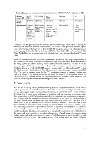
phase). Table 1 summarizes the parameters used to compare and contrast the accelerators.
Table 1: Accelerators and their performance metrics
Accelerator
Name /
Parameter
Intel
Xeon Phi
7290F
NVidia
Titan Xp
DLAU - FPGA TPU (ASICs) PuDianNao
Process
technology
14nm 16 nm N/A 28 nm 65 nm
Area N/A 471 mm N/A, TMMU
takes most of
the area as it
utilize the
highest number
of lookup table
and flipflops
United buffer takes :
29%
Matrix Multiply
Unit:
24%
2 DRAMs each
takes
3%
Host Interface takes
2%
Accumulators 6%
Activation pipeline
5%
Control 2%
Misc I/O 6%
PCIe Interface 3%
3.51 mm2](https://image.slidesharecdn.com/8421mlaij02-220122072044/85/A-SURVEY-OF-NEURAL-NETWORK-HARDWARE-ACCELERATORS-IN-MACHINE-LEARNING-14-320.jpg)
![Machine Learning and Applications: An International Journal (MLAIJ) Vol.8, No.4, December 2021
26
REFERENCES
[1] Li, Zhen, et al. "A survey of neural network accelerators." Frontiers of Computer Science: 1-16.
[2] Wang, Chao, et al. "DLAU: A scalable deep learning accelerator unit on FPGA." IEEE Transactions
on ComputerAided Design of Integrated Circuits and Systems 36.3 (2017): 513-517.
[3] Reagen, Brandon, et al. "Minerva: Enabling low-power, highly-accurate deep neural network
accelerators." Proceedings of the 43rd International Symposium on Computer Architecture. IEEE
Press, 2016.
[4] Zhang, Qian, et al. "ApproxEigen: An approximate computing technique for large-scale
eigendecomposition." Proceedings of the IEEE/ACM International Conference on Computer-Aided
Design. IEEE Press, 2015.
[5] Cruz, Joseph A., and David S. Wishart. "Applications of machine learning in cancer prediction and
prognosis." Cancer informatics 2 (2006): 59.
[6] Zhang, Shijin, et al. "Cambricon-X: An accelerator for sparse neural networks." Microarchitecture
(MICRO), 2016 49th Annual IEEE/ACM International Symposium on. IEEE, 2016.
[7] Gao, Mingyu, et al. "TETRIS: Scalable and Efficient Neural Network Acceleration with 3D
Memory." Proceedings of the Twenty-Second International Conference on Architectural Support for
Programming Languages and Operating Systems. ACM, 2017.
[8] Andri, Renzo, et al. "YodaNN: An Architecture for Ultra-Low Power Binary-Weight CNN
Acceleration." IEEE Transactions on Computer-Aided Design of Integrated Circuits and
Systems(2017).
[9] Guan, Yijin, et al. "FP-DNN: An Automated Framework for Mapping Deep Neural Networks onto
FPGAs with RTL-HLS Hybrid Templates." Field-Programmable Custom Computing Machines
(FCCM), 2017 IEEE 25th Annual International Symposium on. IEEE, 2017.
[10] Chen, Yunji, et al. "Dadiannao: A machine-learning supercomputer." Proceedings of the 47th Annual
IEEE/ACM International Symposium on Microarchitecture. IEEE Computer Society, 2014.
[11] Sze, Vivienne, et al. "Efficient processing of deep neural networks: A tutorial and survey." arXiv
preprint arXiv:1703.09039 (2017).
[12] Chen, Yunji, et al. "DianNao family: energy-efficient hardware accelerators for machine learning."
Communications of the ACM 59.11 (2016): 105-112.
[13] Compton, Katherine, and Scott Hauck. "Automatic design of area-efficient configurable ASIC cores."
IEEE Transactions on Computers 56.5 :662-672.
[14] Ha, Chang-Soo, et al. "ASIC design of IPSec hardware accelerator for network security." Advanced
System Integrated Circuits 2004. Proceedings of 2004 IEEE Asia-Pacific Conference on. IEEE, 2004.
[15] Kuon, Ian, and Jonathan Rose. "Measuring the gap between FPGAs and ASICs." IEEE Transactions
on computeraided design of integrated circuits and systems 26.2 (2007): 203-215.
[16] Wu, Yonghui, et al. "Google's neural machine translation system: Bridging the gap between human
and machine translation." arXiv preprint arXiv:1609.08144 (2016).
[17] TechPowerUp. (2017). NVIDIA TITAN Xp. [online] Available at:
https://www.techpowerup.com/gpudb/2948/titan-xp [Accessed 24 Dec. 2017].
[18] Vanhoucke, Vincent, Andrew Senior, and Mark Z. Mao. "Improving the speed of neural networks on
CPUs." Proc. Deep Learning and Unsupervised Feature Learning NIPS Workshop. Vol. 1.
[19] Shao, Yakun Sophia, et al. "Co-designing accelerators and soc interfaces using gem5-aladdin."
Microarchitecture (MICRO), 2016 49th Annual IEEE/ACM International Symposium on. IEEE,
2016.
[20] Jouppi, Norman P., et al. "In-datacenter performance analysis of a tensor processing unit."
Proceedings of the 44th Annual International Symposium on Computer Architecture. ACM, 2017
[21] Nickolls, John, and William J. Dally. "The GPU computing era." IEEE micro 30.2.
[22] Kołodziej, J., Khan, S. and Burczy'nski, T. (2012). Advances in Intelligent Modelling and Simulation.
Berlin, Heidelberg: Springer Berlin Heidelberg.
[23] Kindratenko, Volodymyr V., et al. "GPU clusters for high-performance computing." Cluster
Computing and Workshops, 2009. CLUSTER'09. IEEE International Conference on. IEEE.
[24] Neil, Daniel, and Shih-Chii Liu. "Minitaur, an event-driven FPGA-based spiking network
accelerator." IEEE Transactions on Very Large Scale Integration (VLSI) Systems 22.12 (2014):
2621-2628.](https://image.slidesharecdn.com/8421mlaij02-220122072044/85/A-SURVEY-OF-NEURAL-NETWORK-HARDWARE-ACCELERATORS-IN-MACHINE-LEARNING-16-320.jpg)
![Machine Learning and Applications: An International Journal (MLAIJ) Vol.8, No.4, December 2021
27
[25] Shao, Yakun Sophia, and David Brooks. "Energy characterization and instruction-level energy model
of Intel's Xeon Phi processor." Proceedings of the 2013 International Symposium on Low Power
Electronics and Design. IEEE Press, 2013.
[26] Chrysos, George. "Intel® Xeon Phi™ coprocessor-the architecture." Intel Whitepaper 176 (2014).
[27] Borkar, Shekhar, et al. "Platform 2015: Intel processor and platform evolution for the next decade."
Technology 1 (2005).
[28] NVIDIA. (2017). NVDIA Developer Resources for Deep Learning and AI. [online] Available at:
https://www.nvidia.com/en-us/deep-learning-ai/developer/ [Accessed 24 Dec. 2017].
[29] Tom's Hardware. (2017). How We Test: Nvidia Titan Xp 12GB. [online] Available at:
http://www.tomshardware.com/reviews/nvidia-titan-xp,5066-2.html [Accessed 24 Dec. 2017].
[30] Intel. (2017). Intel® Xeon Phi™ Processor Competitive Performance. [online] Available at:
https://www.intel.com/content/www/us/en/benchmarks/server/xeon-phi/xeon-phi-competitive-
performance.html [Accessed 4 Dec. 2017].
[31] Guoteng, Pan, et al. "Design and Implementation of a DDR3-based Memory Controller." Intelligent
System Design and Engineering Applications (ISDEA), 2013 Third International Conference on.
IEEE, 2013.
[32] Smith, R. (2017). The NVIDIA GeForce GTX 1080 Ti Founder's Edition Review: Bigger Pascal for
Better Performance. [online] Anandtech.com. Available at:
https://www.anandtech.com/show/11180/the-nvidiageforce-gtx-1080-ti-review/3 [Accessed 4 Dec.
2017].
[33] Software.intel.com. (2017). Optimizing Memory Bandwidth in Knights Landing on Stream Triad |
Intel® Software. [online] Available at: https://software.intel.com/en-us/articles/optimizing-memory-
bandwidth-inknights-landing-on-stream-triad [Accessed 4 Dec. 2017].
[34] Liu, Daofu, et al. "Pudiannao: A polyvalent machine learning accelerator." ACM SIGARCH
Computer Architecture News. Vol. 43. No. 1. ACM, 2015.
[35] Intel. (2017). Intel® Many Integrated Core Architecture - Advanced. [online] Available at:
https://www.intel.com/content/www/us/en/architecture-and-technology/many-integrated-core/intel-
manyintegrated-core-architecture.html [Accessed 4 Dec. 2017].
[36] TechPowerUp. (2017). Intel Xeon Phi SE10X. [online] Available at:
https://www.techpowerup.com/gpudb/1891/xeon-phi-se10x [Accessed 4 Dec. 2017].
[37] Intel.com. (2017). Intel Xeon Phu coprosessor [online] Available at :
https://www.intel.com/content/dam/www/public/us/en/documents/datasheets/xeon-phi-
coprocessordatasheet.pdf [Accessed 4 Dec. 2017].
[38] Software.intel.com. (2017). Intel. [online] Available at: http://software.intel.com/en-us/intel-xeon-
phicoprocessor-workshop [Accessed 4 Dec. 2017].
[39] Zedboard.org. (2017). ZedBoard | Zedboard. [online] Available at:
http://zedboard.org/product/zedboard [Accessed 4 Dec. 2017].
[40] Google Cloud Platform. (2017). Cloud TPUs - ML accelerators for TensorFlow | Google Cloud
Platform. [online] Available at: https://cloud.google.com/tpu/ [Accessed 4 Dec. 2017].
[41] Software.intel.com. (2017). How Intel® Xeon Phi™ Processors Benefit Machine Learning/Deep
Learning Apps and Frameworks | Intel® Software. [online] Available at:
https://software.intel.com/enus/blogs/2016/06/20/how-xeon-phi-processors-benefit-machine-and-
deep-learning-apps-frameworks [Accessed 24 Dec. 2017].
[42] Intel.com. (2017). [online] Available at:
https://www.intel.com/content/dam/www/public/us/en/documents/datasheets/xeon-phi-coprocessor-
x200family-datasheet.pdf [Accessed 24 Dec. 2017].
[43] Chen, Tianshi, et al. "BenchNN: On the broad potential application scope of hardware neural network
accelerators." Workload Characterization (IISWC), 2012 IEEE International Symposium on. IEEE,
2012.
[44] Song, Linghao, et al. "PipeLayer: A pipelined ReRAM-based accelerator for deep learning." High
Performance Computer Architecture (HPCA), 2017 IEEE International Symposium on. IEEE, 2017.
[45] Shi, Weijing, et al. "Algorithm and hardware implementation for visual perception system in
autonomous vehicle: A survey." Integration, the VLSI Journal 59 (2017): 148-156.
[46] Nurvitadhi, Eriko, et al. "Can FPGAs beat GPUs in accelerating next-generation deep neural
networks?." Proceedings of the 2017 ACM/SIGDA International Symposium on Field-Programmable
Gate Arrays. ACM, 2017.](https://image.slidesharecdn.com/8421mlaij02-220122072044/85/A-SURVEY-OF-NEURAL-NETWORK-HARDWARE-ACCELERATORS-IN-MACHINE-LEARNING-17-320.jpg)
![Machine Learning and Applications: An International Journal (MLAIJ) Vol.8, No.4, December 2021
28
[47] Najafi, Mohammadreza, et al. "Hardware Acceleration Landscape for Distributed Real-time
Analytics: Virtues and Limitations." Distributed Computing Systems (ICDCS), 2017 IEEE 37th
International Conference on. IEEE, 2017.
[48] James, Conrad D., et al. "A historical survey of algorithms and hardware architectures for neural-
inspired and neuromorphic computing applications." Biologically Inspired Cognitive Architectures
(2017).
[49] Shafique, Muhammad, et al. "Adaptive and Energy-Efficient Architectures for Machine Learning:
Challenges, Opportunities, and Research Roadmap." VLSI (ISVLSI), 2017 IEEE Computer Society
Annual Symposium on. IEEE, 2017.
[50] Lu, Chien-Ping. "AI, Native Supercomputing and The Revival of Moore's Law." arXiv preprint
arXiv:1705.05983 (2017).
[51] Nurvitadhi, Eriko, et al. "Accelerating recurrent neural networks in analytics servers: comparison of
FPGA, CPU, GPU, and ASIC." Field Programmable Logic and Applications (FPL), 2016 26th
International Conference on. IEEE, 2016.
[52] FPGA, N. (2017). Nallatech 385 – with Stratix V A7 FPGA - Nallatech. [online]
Nallatech. Available at: http://www.nallatech.com/store/fpga-accelerated-computing/pcie-accelerator-
cards/385-a7/ [Accessed 27 Dec. 2017].
[53] Quora.com. (2017). Are neural networks the future of AI? How important are they? | Artificial
Intelligence. [online] Available at: https://www.quora.com/Are-neural-networks-the-future-of-AI-
How-important-are-they [Accessed 27 Dec. 2017].
[54] Reuther, Albert, et al. "Survey of machine learning accelerators." 2020 IEEE High Performance
Extreme Computing Conference (HPEC). IEEE, 2020.](https://image.slidesharecdn.com/8421mlaij02-220122072044/85/A-SURVEY-OF-NEURAL-NETWORK-HARDWARE-ACCELERATORS-IN-MACHINE-LEARNING-18-320.jpg)
A SURVEY OF NEURAL NETWORK HARDWARE ACCELERATORS IN MACHINE LEARNING
- 1. Machine Learning and Applications: An International Journal (MLAIJ) Vol.8, No.4, December 2021 DOI:10.5121/mlaij.2021.8402 11 A SURVEY OF NEURAL NETWORK HARDWARE ACCELERATORS IN MACHINE LEARNING Fatimah Jasem and Manar AlSaraf Department of Computer Engineering, Kuwait University, Kuwait ABSTRACT The use of Machine Learning in Artificial Intelligence is the inspiration that shaped technology as it is today. Machine Learning has the power to greatly simplify our lives. Improvement in speech recognition and language understanding help the community interact more naturally with technology. The popularity of machine learning opens up the opportunities for optimizing the design of computing platforms using well- defined hardware accelerators. In the upcoming few years, cameras will be utilised as sensors for several applications. For ease of use and privacy restrictions, the requested image processing should be limited to a local embedded computer platform and with a high accuracy. Furthermore, less energy should be consumed. Dedicated acceleration of Convolutional Neural Networks can achieve these targets with high flexibility to perform multiple vision tasks. However, due to the exponential growth in technology constraints (especially in terms of energy) which could lead to heterogeneous multicores, and increasing number of defects, the strategy of defect-tolerant accelerators for heterogeneous multi-cores may become a main micro-architecture research issue. The up to date accelerators used still face some performance issues such as memory limitations, bandwidth, speed etc. This literature summarizes (in terms of a survey) recent work of accelerators including their advantages and disadvantages to make it easier for developers with neural network interests to further improve what has already been established. KEYWORDS Artificial Intelligence, ASIC, Convolutional Neural Network, CPU, Deep Learning, Deep Neural Network, FPGA, GPU, hardware accelerators, Intel, Machine Learning, Nvidia, Performance 1. INTRODUCTION AND RELATED WORK Designing a system with the ability to compute on their knowledge from input data to make it perform accordingly is the domain called Machine Learning (ML). [1] In other words, it has the ability to solve complex computations in many networks and make crucial decisions in the form of deep learning. The process of deep learning uses a multi-layer neural network to identify features, which are a combination of unclear abstractions. [2] A neural network is not only a complex system with large amount of neurons, but a complex adaptive nonlinear information processing system which computes on its input through various processing units that have the ability to self-organize, self-adapt and have real-time learning techniques. Neural networks purpose is to estimate uncertainty of inputs to define features. Early neural networks algorithms were conducted on CPU/GPU; however, with the exponential increase in the size of the networks, single CPU/GPU is not enough to handle a network. Therefore, more powerful processors are produced or multiple processors are used for a single network. The use of ML is growing exponentially around the world, and its users are expecting optimal results and high performance of functionality. Machine learning is highly used in medical practices. Advances in medical imaging enabled by machine learning can increase the accuracy of medical diagnosis and expand access to care ultimately saving lives. In addition, machine
- 2. Machine Learning and Applications: An International Journal (MLAIJ) Vol.8, No.4, December 2021 12 learning can be applied to cancer prognosis and prediction, which in the near future, may be used as personalized, predictive medicine to avoid or minimize cancer diagnosis. [5]. However, its architecture still faces some problems due to the increasing size of the neural networks for obtaining higher accuracy, which may reduce the overall performance of the networks in terms of power and speed in addition to overhead costs. [7] Neural networks in its several forms are one class of algorithms used for ML. Some examples of neural networks include Artificial Neural Networks (ANN), Convolutional Neural Networks (CNN), and Deep Neural Networks (DNN). [1] CNN have been giving accurate results in difficult tasks such as image and speech recognition. Also, more complicated applications such as face detection. However, CNN are not completely able to neglect the power constraints of mobile and Internet of Things (IoT) devices, which are exponentially increasing its availability in the market. Furthermore, replacing all the CNN computations from the IoT devices to data servers requires high power consumption due to the transmission of data streams (high bandwidth is required) [8]. DNN algorithms have gained extreme popularity in the past decade for its high achievement in everyday applications such as speech recognition, computer vision, and natural language processing. The success of DNN can be summarized under three main points namely, availability of massive datasets, access to parallel computational resources and improvements allowing DNN modifications to data [3]. However, DNNs are identified as computationally and memory intensive as their architectures are made of multiple layers with extremely large numbers of connections made of neurons, which increases complexity. [6] Thus, it is somewhat challenging to use DNN in large-scale data centers and real-time embedded systems. [9] A wide variety of hardware accelerators have been proposed for ML applications which will be explained in the next section. 2. RELATED WORK Minerva, a highly-accurate deep neural network accelerator produced by Reagen et al. is designed and built to optimize hardware accelerators by achieving minimal power consumption; keeping in mind maintaining high prediction accuracy. [3] Minerva reduces overall power consumption across five diverse machine learning datasets by optimizing data types, reducing unnecessary computations and lowering SRAM voltages. Zhang et al. proposed ApproxEigen, a computing technique for large-scale eigen-decomposition to find finite number of eigenvalues and eigenvectors for positive semi-definite symmetric matrices. This method can be applied in search engines where less energy is consumed and within high quality restrictions. [4] Zhang et al. proposed an accelerator named Cambricon-X that is not only effective in dense neural networks, but also sparse neural networks. This accelerator is able to perform more than 15 output neurons with sparse connections simultaneously and increase accuracy by developing and manipulating abnormality of neural networks. This accelerator is based on the Processing Elements (PE) architecture which in return, achieves 7.23x and 6.43 better performance and energy efficiency respectively than the general DianNao accelerator. [6] Gao et al. created Tetris, a scalable architecture with #D-stacked memory for neural network inference. The relatively high performance and low energy consumption is achieved in this type of architecture by rebalancing the use of area for processing elements and SRAM buffers in addition to in-memory accumulation features. [7]
- 3. Machine Learning and Applications: An International Journal (MLAIJ) Vol.8, No.4, December 2021 13 Albert Reuther in his paper [54] mentioned the importance of machine learning accelerators focusing on the CPU and GPU accelerators, creating a benchmark for testing them. In addition to that he revealed some new accelerators that will be announced in the future such as: Cloud AI 100 accelerators created by Qualcomm, CloudBlazer T10 announced by Enflame company and Maxion CPU AI processor built by Esperanto. Reuther gave a look at the future of machine learning accelerators. Since there’s an absence in voltage scaling, only some transistors on a chip will be used simultaneously in the future, which is known as coined Dark Silicon. This mechanism risks many-cores and massive onchip parallelism due to simultaneously tracking. Therefore, there’s a new mechanism named customization which solves the above mentioned problem. This mechanism involves embedding a chip with accelerators for more efficient execution (instead of dividing each algorithm of a program into smaller algorithms, [43] Hence, the use of hardware accelerators is an essential step towards a brighter future. As a result, to reduce the above mentioned problems, some accelerators have been implemented such as Field-Programmable Gate Array (FPGA), Application Specific Integrated Circuit (ASIC) and Graphic Processing Unit (GPU). The FPGA and ASIC have somehow a better performance in terms of power consumption compared to the GPU; however, they both have limited computing resources, memory, and I/O bandwidths. [2] Although these may be considered disadvantages and may reduce the performance of the accelerators, it is still possible to use them in several applications such as Siri, and Google now in Apple, iPhoto or Google Picasa etc. [10] The main purpose of this paper is to compare the proposed architectures of recent designed accelerators in machine learning and evaluate their performance. The rest of this paper is structured as follows. First, Section 2 and 3 briefly introduces CNNs and DNNs including their implementations then reviews the different type of accelerators. Section 4 evaluates the accelerators of machine learning in various performance metrics. Finally, a conclusion is discussed in Section 5. 3. BACKGROUND In this section, we present an overview of two classes of neural networks, namely CNN and DNN including their architecture with all the layers and the functions. Moreover, how the input is generated and the output is retrieved using the components of these neural networks are also reported. In addition, some simple applications that use these types of neural networks are mentioned. 3.1. CNN CNN has the most suitable architecture for image applications and the applications based on the implicit translation invariance properties of their convolutional layers [10]. CNN are composed of multiple layers where each layer generates a higher level abstraction of input data these abstractions are called feature map (fmap) which preserve exclusive information. CNN are able to have high performance by employing a very deep hierarchy of layers. Each convolutional layer in the architecture of the CNN is composed of high dimensional convolutions. This convolution is based on a set of 2D input feature maps (ifmaps) named as a channel. The results of the convolutional layer at each point are added to the filtering results. The result of this addition is one channel of output feature map (ofmap). More output channels can be created on the same input by stacking other 2D filters. To improve the reuse of the filters weights, multiple stacks of input features may be processed together as a batch.
- 4. Machine Learning and Applications: An International Journal (MLAIJ) Vol.8, No.4, December 2021 14 3.2. DNN DNNs can be used in a wide range of applications such as speech recognition and web search regardless of its complexity in the design of the conventional layer. For DNN’s to be used in AI systems, it must improve the energy efficiency and throughput without having drawbacks in performance or increasing the hardware cost [11]. DNN’s architecture is made of four types of layers which are: pooling layers (POOL), convolutional layers (CONV), classifier layers (CLASS), and local response normalization layers (LRN). The POOL, CONV, LRN layers may alternate in their positions; however, the CLASS layers are always at the end of the sequence. The CONV layer is responsible for the implementation of a set of filters to recognize the characteristics elements of the input data. The filter is defined by co-efficient that form a kernel which are further used in a learning technique to form the layer weights. POOL layers: The POOL layer is responsible for the computation of the maximum or average of the neighbor points to further analyze the input data. By doing such computation, the input dimensionality is reduced to allow larger scale features to be computed and easier to be identified in the next layers. LRN: The LRN layer is responsible for the competition between neurons at the same location, but different neighbor feature maps. CLASS: The CLASS layer is simply the result of the whole process including all other three layers (CONV, POOL, LRN) put together. This layer has the lowest number of inputs due to the dimensionality reduction of the pooling layers. The main role of this layer is to combine the features form the previous layers with their outputs. [10] 3.3. Energy-Efficient Hardware Accelerators In this section, we present different types of accelerators that are used to enhance neural networks in the past years. Few of these accelerators may be classified into four main categories, DianNao Family, Field Programmable Gate Array (FPGA), Application Specific Integrated Circuit (ASIC) and general-purpose processors. Figure 1 shows the structure and breakdown of the accelerators mentioned in this paper. Figure 1. Accelerator breakdown 3.3.1. DianNao Family The DianNao family accelerators are a series of hardware accelerators designed for ML (especially neural networks), with a special emphasis on the impact of memory on the accelerator design, performance, and energy.
- 5. Machine Learning and Applications: An International Journal (MLAIJ) Vol.8, No.4, December 2021 15 3.3.1.1. DianNao: Neural Network Accelerators DianNao is the first member in the DianNao family. Its purpose is to fully utilize arithmetic elements of data in memory. However, its main concern is to balance between minimal memory transfers and higher performance for neural networks depending on the number of arithmetic units, memory policy, and the structure and amount of on-chip RAMs. The block diagram of DianNao is shown in Figure 2. Figure 2. Block diagram of DianNao accelerator The architecture of this accelerator is advantageous in several ways. First, multiple outputs are computed simultaneously to exploit spatial locality (by implementing Direct memory access) of data and reduce the number of accesses to buffers. Second, the storage of data is divided into the three buffers which is beneficial as it avoids data conflicts and allows reuse input neurons in the input buffer. In addition, each of these buffers have different data types and; therefore, have different characteristics (read width and different distance); hence, splitting the buffers is needed to adjust the memory to the corresponding read/write width. [12] As shown in the figure DianNao the synaptic weights buffer (SB) is connected to a computational block performing the hidden synapses and neurons computations which called the Neural Functional Unit (NFU). The computations at the NFU can be executed in either two or three stages depending on the layer type. 3.3.1.2. DaDianNao: Machine Learning Super Computer Accelerators Nowadays, there is an increase in interest towards large neural networks. Although the above mentioned accelerator can execute neural networks at more than one scale, it still needs a storage for the neuron values in main memory when dealing with larger neural networks. Accessing main memory more frequently limit the performance and energy efficiency of DianNao. In DaDianNao having the following design principles solves this issue. The first step is to create a new design where synapses are always stored nearby the neurons to save time and energy since there is less data movements. This type of design can be used when there is no main memory. The second step is to create a symmetric architecture where each node mark is massively biased towards storage rather than computations. The third step is to only transfer values with less number of
- 6. Machine Learning and Applications: An International Journal (MLAIJ) Vol.8, No.4, December 2021 16 layers in terms of magnitude and bandwidth (neurons rather than synapses values). The fourth and last step is to break down the storage into smaller ones to allow high internal bandwidth. [10] The DaDianNao’s design is based on a set of nodes, one per chip, identical and arranged in mesh topology. Each node contains significant storage and neural computational units (the classic pipeline of multipliers, added tree and nonlinear functions implemented via linear interpolation), which is called the NFU to be consistent with the DianNao accelerators. The key characteristics of the nodes architecture in DaDianNao is designed as follows: Tile-based organization: All functional units (adders, multipliers) are put together in a single computational block (NFU). However, if the NFU is significantly scaled up the data movements between it and the onchip storage will require a very high internal bandwidth resulting in a wiring overhead. To solve the problem, a tile-based organization is applied for each node. Each tile consists of NFU and 4 RAM banks to store synapses between neurons as shown in Figure 3. [12] Figure 3. Tile organization 3.3.1.3. PuDianNao: Polyvalent Machine Learning Accelerators Neural network accelerators in machine learning field have been performing effectively in some of the applications such as pattern recognition. However, users need an accelerator that is more applicable in different domains for better performance and higher accuracy. Hence, The PuDianNao accelerator could be used which is known for its various representative ML algorithms (i.e., k-nearest neighbors, k-means, linear regression, vector machine, deep neural network and classification tree). The architecture design of PuDianNao design is divided into two main parts, namely, execution unit and memory hierarchy that are responsible for the computations and structure characteristics of machine learning, respectively. [1] The main components of this type of accelerator are functional units, data buffers, a control module, instruction buffer and a DMA. The role of a functional unit is to complete the most recurrent operations in a manner way. The first component of this design (functional unit) is divided into a machine learning unit (MLU) that is used for supporting computational computations and an arithmetic logic unit (ALU). The architecture of the PuDianNao is shown in Figure 4. [12]
- 7. Machine Learning and Applications: An International Journal (MLAIJ) Vol.8, No.4, December 2021 17 Figure 4. Architecture of PuDianNao accelerator 3.3.2. Field-Programmable Gate Array Other than the accelerators described previously in this paper, an FPGA can also be used to accelerate computer intensive applications like CNNs as it provides large amount of logic resources. [1] Some advantages of FPGAs include its programmability and configurability that allows a custom design to be evaluated in a short period of time; hence, it reduces the time and expenses to develop such a design. However, FPGAs have a lower performance-energy efficient than Application Specific Integrates Circuit (ASIC). In addition, most FPGAs available today focus on implementing a particular deep learning algorithm efficiently, but their architectures cannot be modified with change in network size or network topologies. [2] One The main accelerator that are implemented using FPGAs is called DLAU. DLAU is a scalable accelerator implemented using FPGA as the hardware platform. [2] This accelerator focuses on improving the performance and maintain low power cost by employing three pipelined processing units to enhance the overall throughput and make full usage of tile techniques to apply locality for machine learning applications. The processing units are as follows: - Tiled Matrix Multiplication Unit (TMMU) purpose is to handle the multiplication and accumulation operations. In addition, it can explore data locality of the weights and is responsible for the Part sum. - Part Sum Accumulation Unit (PSAU) purpose is to accumulate the part sum produced by the previous processing unit (TMMU). Once there are no more values to accumulate, the PSAU sends the result to the AFAU. - Activation Function Acceleration Unit (AFAU) purpose is to implement the activation function with almost no accuracy loss. DLAU architecture is made of four basic components namely, embedded processor, DDR3 memory controller, a DMA module, and the DLAU accelerator itself.
- 8. Machine Learning and Applications: An International Journal (MLAIJ) Vol.8, No.4, December 2021 18 A. Embedded processor: Provides an interface to the users and allows communication with the DLAU. Transfers the weight matrix and input data to internal BRAM blocks, to trigger the DLAU accelerator and return the final output to the user. B. DLAU accelerator: Accommodates different applications as it is flexible and can adapt to different scenarios. 3.3.3. Applications Specific Integrated Circuits The application specific integrated circuits (ASICs) is known for its ease of use in terms of flexibility and customization in design. An ASIC is meant to develop hardware to solve a problem by building gates to emulate the logic. These chips are best at performance regardless of its little programmability at a given power and cost budget. In order to meet the specific needs of consumers, ASICs in batch production and universal integrated circuits used to be smaller volume, lower power consumption, reliability improved, higher performance, security enhanced and lower cost (14). This type of design started in 1990s in many useful applications (i.e. mobile phones). Also, its price was reduced with time for such applications. [13] ASICs are known for its highest computation in efficiency of all other types for targeted applications. They are harder in computation compared to GPUs and FPGAs. [15] Another disadvantage over the others is its high cost when needed to be built and therefore might become old-fashioned as algorithmic advances become available. [14] At the meantime, only Google have developed an ASIC for M. however, some other startups are creating their own ASIC for this market over the next coming years. [16] Google Tensor Processing Unit (TPU) In May 2016, Google working labour announced the Tensor Processing Unit (TPU) which is a custom ASIC that is created only for ML. TPU is specifically used in ML applications which allows the chip to accept reduced computational precision, hence, fewer transistors per operation are required. Therefore, Google allows more operations per second into the silicon, use enhanced ML models and apply these models more quickly, so users get more accurate results faster. A TPU can fit into a hard disk drive slot in Google’s data center racks. [16] The TPU ASIC is built on a 28nm process, runs at 700MHz and consumes 40W when running. Because Google needed to deploy the TPU to Google's existing servers as fast as possible, they chose to package the processor as an external accelerator card that fits into an SATA hard disk slot for drop-in installation. The TPU is connected to its host via a PCIe Gen3 x16 bus that provides 12.5GB/s of effective bandwidth. [20] The TPU includes the following computational resources: - Matrix Multiplier Unit (MXU): 65,536 8-bit multiply-and-add units for matrix operations - Unified Buffer (UB): 24MB of SRAM that work as registers - Activation Unit (AU): Hardwired activation functions In the case of the TPU, Google designed its MXU as a matrix processor that processes large number of operations at a single clock cycle. To implement such a large-scale matrix processor, the MXU uses a systolic array as its architecture rather than typical CPUs and GPUs architectures. CPUs are designed to run almost any calculation as they are considered general-purpose computers. To implement this generality, CPUs store values in registers, and a program instructs the Arithmetic Logic Units (ALUs) which registers to read, the operation to perform (such as an addition, multiplication or logical AND) and the register into which to put the result. A program consists of a sequence of these
- 9. Machine Learning and Applications: An International Journal (MLAIJ) Vol.8, No.4, December 2021 19 read/operate/write operations. All of these features that support generality (registers, ALUs and programmed control) have costs in terms of power and chip area. For an MXU, however, matrix multiplication needs to use the inputs several times to reach the final output. The input value is read only once, but used for many different operations without storing it back to a register. Wires only connect spatially adjacent ALUs, which makes them short and energy-efficient. The ALUs perform only multiplications and additions in fixed patterns, which simplifies their design. The design is called systolic due to the data having a wave flow just like the way that the heart pumps blood. This is an advantage as the power is optimized and area consumption is more efficient in performing matrix multiplications. From an engineer point of view, this architecture limits number of registers, controls and allows operational flexibility in exchange for efficiency and allows higher operation density. The TPU Matrix Multiplication Unit has a systolic array mechanism that contains 256 × 256 = total 65,536 ALUs. That means a TPU can process 65,536 multiply-and-adds for 8-bit integers every cycle. Because a TPU runs at 700MHz, a TPU can compute 65,536 × 700,000,000 = 46 × 1012 multiply-and-add operations or 92 Teraops per second (92 × 1012) in the matrix unit. [20]. Figure 5 shows the components of the TPU die and what percentage each components takes from the overall area of the die. Figure 5. TPU Die component 3.3.4. CPU/GPU Accelerators and Processors Training and prediction phase of neural networks are performed on general-purpose processors like CPU and Graphic Processing Units (GPU). There are many types of tools, which provide relatively complete programming environment for neural networks on CPU/GPU. [1] GPUs have been the subject of extensive research during the last few years and have been successfully applied to general-purpose applications out of the graphical domain. The GPUs can complete many floating point operations per second on their large bandwidth on-board memory. [17] Compared with the GPU, CPU clusters waste a lot of resources on communication between cores even if they are candidates for sparse or networks beyond memory volume of GPU. GPUs employ the fundamentally different SPMD (Single Program Multiple Data) architectures and are specialized for intense highly parallel computations. Considering these properties of algorithms, GPUs exceed CPUs in CNNs and DNNs. GPUs have not only more generality, but also higher performance than CPUs. Researchers are conducted to fully explore how faster GPUs are able to accelerate machine learning algorithms over CPUs. [1]
- 10. Machine Learning and Applications: An International Journal (MLAIJ) Vol.8, No.4, December 2021 20 3.3.4.1. NVidia Titan Xp GPU Titan Xp is considered the fastest accelerator among all other accelerators for DNN training on a desktop PC based on the NVIDIA Pascal architecture [28]. It was launched in April 2017. The TITAN Xp is a highend graphics card by NVIDIA. Created on a 16 nm process, and based on the GP102 graphics processor, in its GP102-450-A1 variant, the chip supports DirectX 12.0. The GP102 graphics processor is a large chip with a die area of 471 mm² and 12,000 million transistors. It contains 3840 shading units, 240 texture mapping units and 96 ROPs. NVIDIA has placed 12,288 MB GDDR5X memory on the card, which is connected using a 384-bit memory interface. The GPU is operating at a frequency of 1405 MHz, which can be boosted up to 1582 MHz, memory is running at 1426 MHz [17]. This chip is a dual-slot card, which can draw power from 1x 6-pin + 1x 8-pin power connectors, with power draw rated at 250 W. Display outputs include: 1x DVI, 3x Display Port. TITAN Xp is linked to the rest of the system using a PCIe 3.0 x 16 interfaces. The card measures 267 mm in length, and features a dual-slot cooling solution. All 30 of the processor’s SMs are enabled, yielding 3840 CUDA cores and 240 texture units. Using the appropriate equipment to calculate compute performance, Titan Xp measured a rate of roughly 10.8 TFLOPS [29]. 3.3.4.2. Intel Processors Xeon Phi CPU Nowadays, most processors being created exploit thread level parallelism (TLP) for seeking higher performance. Hence, multicore/multithread processors are immensely entering the market and are becoming the dominant architectures used in many applications such as mobile platforms and other high performance computing (HPC) systems. In addition, as technology increases, the number of transistors available will continue to grow generation after generation. To fully utilize those transistors and further make full potential of TLP, architecture developers’ will further design multicore chips. [25] The Software developers of Xeon Phi created an instruction level energy model to evaluate and optimize the energy – efficient software. To create such model, energy consumption of the processor was characterized under three main categories by showing how energy per instruction scales with number of cores, number of threads per core and different instruction types to further optimize the energy efficiency. This architecture can test the energy consumption using software code which is an important step for software developers and allows them to minimize energy cost. In addition, this model only needs performance counter statistics as input, which existing software profiling tools already provide to verify the energy consumption. [25] Intel processors work in such a way that tasks are broken down into many concurrent operations and are distributed among many small processing units. This technique achieves higher performance by executing many operations in parallel at more reasonable clock rates rather than carrying out a few tasks in a serial manner at an extremely high frequency. This is achieved by activating only the cores needed for a given task, while idle cores are powered down. This controlled processing resources allows the chip to use only dedicated power. The advantages of such Intel architectures is the reduction in leakage current, reduced mismatches between core performance and memory speed. Also, bottlenecks are also reduced. Moreover, Intel are trying to create new processors that allow dynamic reconfiguration of the cores, interconnects and caches to meet diverse and changing requirements due to growing technology. [27] The coprocessor of the Intel Xeon Phi family has the following features: - A processor with up to 72 cores and 16 GB high bandwidth on package MCDRAM memory. - Intel C610 Series Platform Controller Hub (PCH) with x4 DMI PECI
- 11. Machine Learning and Applications: An International Journal (MLAIJ) Vol.8, No.4, December 2021 21 - Non-transparent Bridge (NTB) linking the processor to the edge connector. - X16 PCI Express Gen3 interface with SMBus management interface. - SMC, thermal sensors, - More than 12V power monitoring and on-board fan PID controller on the active SKU - Coprocessor-level RAS features and recovery capabilities. - On-board flash device [42] 3.3.5. Others Some other accelerators are listed below which do not fit under a specific category: 3.3.5.1. Cambricon X As mentioned in all the sections above, Neural networks (NNs) are useful in a many different applications. For example, image recognition and automatic translation. NNs can be both computationally and memory intensive, as it they have a very deep structure, with multiple layers of neurons and connections (i.e., synapses). There are also sparse NNs which are an effective solution to reduce the amount of computation and memory required. Although existing NN accelerators can professionally process dense and regular networks, they cannot benefit from the reduction of synaptic weights. Cambricon X is an accelerator that uses a multiple processing elements (PE) architecture companied with a buffer controller (BC), so as to manage the irregularity of NN models. Specifically, the BC integrates an efficient indexing module to select the dedicated neurons only from the neuron buffers, and then transfer such neurons to connected PEs with less bandwidth requirement. After receiving such neurons, the PEs can perform efficient computations with locally stored compressed synapses. Moreover, due to irregular distribution of synapses, multiple PEs can work in an asynchronous system to enhance overall performance. [6] Cambricon X architecture shown in Figure 6, consists of a control processor (CP), a buffer controller (BC), two neural buffers (NBin and NBout), a direct memory access module (DMA) and a computation unit (CU) which contains multiple processing elements (PEs). All the PEs are connected as a Fat-tree topology in order to avoid bottleneck. The BC selects needed neurons for each PE from local neuron buffers based on the loaded instructions, which are decoded by the CP, and transfers those neurons to PEs for efficient local computation. The advantage of this architecture is the indexing unit in the BC. [6]
- 12. Machine Learning and Applications: An International Journal (MLAIJ) Vol.8, No.4, December 2021 22 Figure 6. Cambricon-X accelerator architecture and buffer controller architecture Since hardware cost is always on the top of the designer’s mind, this design uses 16-bit fixed- point arithmetic units rather than conventional 32-bit floating-point units to reduce hardware cost. The BC is designed to transfer dedicated neurons to PEs, allowing computations on PEs, and performing less computation-intensive tasks. The architecture of the BC consists of a module used to index data for computation based on connections (Indexing Module, IM), and the specialized function units for the BC (BCFU). At first, inputs are fetched from NBin based on the control signals decoded from instructions. Then, either the needed neurons are selected from the inputs and transferred to each PE or the inputs are directly fed into the BCFU. 3.3.5.2. Tetris with 3D memory TETRIS is an NN accelerator optimized to be used with state of-the-art 3D memory stacks. The architecture used allows for near-data processing to transfer parts of the NN computations into the memory system. Micron’s Hybrid Memory Cube (HMC) is used as the 3D memory. The hardware architecture of TETRIS is built such that the HMC is stacked vertically and divided into sixteen 32-bit-wide vaults, which is similar to conventional DDRx channels and can be accessed independently. The vault channel bus uses TSVs to connect all DRAM dice to the base logic die. Each DRAM die contains two banks per vault. Each bank is an array of DRAM cells. In the terms of data access, the global data lines transfers data locally (DRAM cell arrays) to the universal sense-amplifiers (SAs) at the bottom of the bank, which strengthens it and send it back to the channel TSV data bus to its final destination. Although accesses to different banks can overlap at some point, all banks in a vault share the same TSVs. [7]
- 13. Machine Learning and Applications: An International Journal (MLAIJ) Vol.8, No.4, December 2021 23 4. EVALUATION In order to evaluate the overall performance of the mentioned accelerators in the previous section, we have surveyed the available specifications of all the accelerators in more than one parameter. This section contains a discussion of the performance, architecture, memory bandwidth, the process technology, the area and the power of each type of accelerator. Furthermore, future trends 4.1. Architecture/Performance Discussion Measuring the performance can be very critical for neural accelerators, because of the varying testing benchmarks and applications. However, this section shall briefly distinguish between the different accelerators and shall aid in the decision of which accelerator should be used in each field. Starting off with the GPUs, they are used for graphic processing tasks. For example, GPUs are driven by the real-time performance requirements for complex and high-resolution 3D scenes in computer games where a high number of instructions are executed in parallel due to enhancement of the GPUs in the past decade. In addition, general purpose GPUs are used in high performance computing (HPC). Furthermore, it has been achieving high performance in scientific applications also due to its thousands of parallel processors. These processors can achieve higher throughput than CPUs when running parallel algorithms. Many of the ML algorithms require architectures similar to GPUs’ architecture due to the need of highly parallel executions. For example, CNNs’ evaluation is controlled by the convolutional operations between the neuron layers and a number of spatial filters, which can be accelerated, with the use of GPUs. Therefore, some deep learning tools (such as OpenCV and Caffe) have taken advantage of GPU to improve the overall performance. This is why many autonomous vehicles use GPUs; however, GPUs consume high energy and has high power consumption. Some GPU chips can improve their power efficiency by optimizing its computing cores, reorganizing its GPU architecture, improving memory compression, and adopting minimal process technology. [45] As compared to GPUs and CPUs, FPGAs improve the computing efficiency and reduces energy consumption. FPGA-based design is often described by hardware description language (HDL) such as VHDL. The design is specified at register-transfer level (RTL) by registers and combinational logics between the registers. FPGAs are low-level abstractions and the designers must be very precise when designing the hardware architecture and maintain the massive concurrency between different hardware modules. Nowadays, with the advance of high-level synthesis, FPGA designers can use high-level specifications. This advance reduces the overall cost and shortens the time-to-market. If an FPGA is appropriately optimized, it would be more energy efficient than both CPUs and GPUs for a variety of computer vision algorithms such as optical flow, local image feature extraction etc. The energy efficiency conclusion is measured in terms of the throughput over the power consumed. [45] Also, the FPGAs are somehow different than GPUs where FPGAs have a pipelined hardware architecture and the latter has a massive parallel SIMD architectures to enhance their throughput. [2] With the newest accelerators, ASICs have demonstrated better performance and utilization compared to FPGAs due to its truly custom implementations that leads to higher efficiency. ASIC accelerators contains simply just the necessary FMA hardware units needed whereas the FPGAs use only around 70 % of the DSPs available (utilization) due to routing constraints. Results show that ASICs are approximately 7 times more efficient when using the same process technology than FPGAs. [51] Other than the performance and hardware complexity, the price of the accelerator is a critical issue for
- 14. Machine Learning and Applications: An International Journal (MLAIJ) Vol.8, No.4, December 2021 24 accelerator developers. For example, Intel Xeon Phi 7290F costs $3368, which is considered very expensive for beginners. [42] NVidia Titan Xp is almost 1/3 of Intel’s accelerator price ($1200). [28] As of the DLAU- FPGA accelerator, the hardware cost depends only on the tile size, which saves significant number of hardware resources. [2] However, the newest FPGA accelerator types with their new enhancements are becoming extremely expensive. For example, the newest FPGA costs $4995. [52] Google’s TPU cloud did not announce the official cost; however, they offered cloud services training prices. GPUs are almost the same as multi-core CPUs but with two differences. First, GPUs have better throughput whereas CPUs are greater in speed. Also, CPU improves the execution of a single instruction thread whereas GPUs take the opposite route obtaining benefits from a larger number of threaded streams. The second difference is how threads are scheduled. The operating system allows threads over different cores of a CPU in a pre-emptive manner; whereas, GPUs have dedicated hardware for the cooperative scheduling of threads. [22] 4.2. Other Performance Metrics and What Do they Represent Memory bandwidth is an important performance metrics as it shows the rate at which data can be read or stored from memory. Developers of applications need to consider this type of specification if the speed is a crucial factor. In addition, the higher the memory bandwidth available, the less likely a bottleneck would occur. Moreover, the size of the process technology matters as the smaller the size of the components needed on a chip; the more transistors will fit. Hence, parallelism can be exploited more efficiently which results in a faster execution. Other than the cost of production, the area of the chip is fundamental for efficiency in more than one perspective. As the smaller the die size, the more dies can be equipped on a chip. Lastly, power is considered the main factor in deciding how much components you can build on a chip; therefore, it is very important to determine the power consumption of each accelerator (i.e. in the designing phase). Table 1 summarizes the parameters used to compare and contrast the accelerators. Table 1: Accelerators and their performance metrics Accelerator Name / Parameter Intel Xeon Phi 7290F NVidia Titan Xp DLAU - FPGA TPU (ASICs) PuDianNao Process technology 14nm 16 nm N/A 28 nm 65 nm Area N/A 471 mm N/A, TMMU takes most of the area as it utilize the highest number of lookup table and flipflops United buffer takes : 29% Matrix Multiply Unit: 24% 2 DRAMs each takes 3% Host Interface takes 2% Accumulators 6% Activation pipeline 5% Control 2% Misc I/O 6% PCIe Interface 3% 3.51 mm2
- 15. Machine Learning and Applications: An International Journal (MLAIJ) Vol.8, No.4, December 2021 25 Memory Bandwidth 115.2 GB/s 547.6 GB/s N/A DDR3 34 GB/s N/A Power (TDP) 260 Watt 250 Watt 234 mWatt 75 Watt 596 mWatt Performance Processor base frequency is 1.50 GHZ (1.5 billion cycles per second) Floatingpoint performance: 12,150 GFLOPS Computes 32 hardware neurons with 32 weights every cycle. The clock cycle is 200MHz 180 teraflops 1.056 trillion operation per second The Intel Xeon Phi processor has the smallest process technology, which refers to having the possibility of maximum number of transistors. The Nvidia Titan processor has the highest bandwidth referring to fast delivery of data. The DLAU dissipates least power when operating at base frequency. In fact, the DLAU dissipates x1000 less than the Intel Xeon Phi and the Nvidia Titan. The PuDianNao is also considered to dissipate low power compared to both CPUs and GPUs. As for the memory limitations and issues; the DianNao Accelerates force loop tiling to minimize the memory access which efficiently accommodates large neural networks. Overall in DianNao the titling techniques reduces memory bandwidth for over 50% reduction. For Intel Xeon the memory supports ECC memory which can detect and correct types of internal data corruption. The Titan Xp uses a 12 GB of GDDR5X memory operating at 1.426 GHz, and uses 384 bit bus, the effective memory bandwidth is 547.58 GB/s that causes a maximum power draw around 250 Watt. The required memory usage for the TPU exceeds the amount of memory required on a GPU or CPU due to the padding used when designing the layers of the accelerator. Finally the DLAU accelerators relies of buffers, and pipelines to minimize memory transfer operations, and reuse the computing units to implement the large size neural networks. 5. CONCLUSION With the rise of the big data era, the Internet daily produces a huge amount of data that is needed with deep learning and artificial intelligence. In addition to the exponential growth of the smart phones technologies, more complicated neural networks are applied to solve several problems. Therefore, how to speed up the techniques of neural network are becoming an important issue; thus, investigating in it will help understanding how it works and what architectures the designers use to keep up with the growth in the machine learning field. In this article, we introduced two of the most famous neural networks with their implementations. Furthermore, we described in details some of the accelerators used to enhance the neural networks. The accelerators include their architectures configuration and how they are implemented in such a way to ensure a speed up. Finally, the accelerators used have been evaluated in more than one perspective and compared and contrasted among them, which makes it easier for developers to choose among the most suitable accelerator depending on which metric is crucial and which metric can be tolerated. For the future work we are planning to investigate of more types of accelerators with new aspects that include testing each and observe the performance of each. In addition to testing the affect of each components on the performance for example the sizes of the buffers, inputs and number of layers.
- 16. Machine Learning and Applications: An International Journal (MLAIJ) Vol.8, No.4, December 2021 26 REFERENCES [1] Li, Zhen, et al. "A survey of neural network accelerators." Frontiers of Computer Science: 1-16. [2] Wang, Chao, et al. "DLAU: A scalable deep learning accelerator unit on FPGA." IEEE Transactions on ComputerAided Design of Integrated Circuits and Systems 36.3 (2017): 513-517. [3] Reagen, Brandon, et al. "Minerva: Enabling low-power, highly-accurate deep neural network accelerators." Proceedings of the 43rd International Symposium on Computer Architecture. IEEE Press, 2016. [4] Zhang, Qian, et al. "ApproxEigen: An approximate computing technique for large-scale eigendecomposition." Proceedings of the IEEE/ACM International Conference on Computer-Aided Design. IEEE Press, 2015. [5] Cruz, Joseph A., and David S. Wishart. "Applications of machine learning in cancer prediction and prognosis." Cancer informatics 2 (2006): 59. [6] Zhang, Shijin, et al. "Cambricon-X: An accelerator for sparse neural networks." Microarchitecture (MICRO), 2016 49th Annual IEEE/ACM International Symposium on. IEEE, 2016. [7] Gao, Mingyu, et al. "TETRIS: Scalable and Efficient Neural Network Acceleration with 3D Memory." Proceedings of the Twenty-Second International Conference on Architectural Support for Programming Languages and Operating Systems. ACM, 2017. [8] Andri, Renzo, et al. "YodaNN: An Architecture for Ultra-Low Power Binary-Weight CNN Acceleration." IEEE Transactions on Computer-Aided Design of Integrated Circuits and Systems(2017). [9] Guan, Yijin, et al. "FP-DNN: An Automated Framework for Mapping Deep Neural Networks onto FPGAs with RTL-HLS Hybrid Templates." Field-Programmable Custom Computing Machines (FCCM), 2017 IEEE 25th Annual International Symposium on. IEEE, 2017. [10] Chen, Yunji, et al. "Dadiannao: A machine-learning supercomputer." Proceedings of the 47th Annual IEEE/ACM International Symposium on Microarchitecture. IEEE Computer Society, 2014. [11] Sze, Vivienne, et al. "Efficient processing of deep neural networks: A tutorial and survey." arXiv preprint arXiv:1703.09039 (2017). [12] Chen, Yunji, et al. "DianNao family: energy-efficient hardware accelerators for machine learning." Communications of the ACM 59.11 (2016): 105-112. [13] Compton, Katherine, and Scott Hauck. "Automatic design of area-efficient configurable ASIC cores." IEEE Transactions on Computers 56.5 :662-672. [14] Ha, Chang-Soo, et al. "ASIC design of IPSec hardware accelerator for network security." Advanced System Integrated Circuits 2004. Proceedings of 2004 IEEE Asia-Pacific Conference on. IEEE, 2004. [15] Kuon, Ian, and Jonathan Rose. "Measuring the gap between FPGAs and ASICs." IEEE Transactions on computeraided design of integrated circuits and systems 26.2 (2007): 203-215. [16] Wu, Yonghui, et al. "Google's neural machine translation system: Bridging the gap between human and machine translation." arXiv preprint arXiv:1609.08144 (2016). [17] TechPowerUp. (2017). NVIDIA TITAN Xp. [online] Available at: https://www.techpowerup.com/gpudb/2948/titan-xp [Accessed 24 Dec. 2017]. [18] Vanhoucke, Vincent, Andrew Senior, and Mark Z. Mao. "Improving the speed of neural networks on CPUs." Proc. Deep Learning and Unsupervised Feature Learning NIPS Workshop. Vol. 1. [19] Shao, Yakun Sophia, et al. "Co-designing accelerators and soc interfaces using gem5-aladdin." Microarchitecture (MICRO), 2016 49th Annual IEEE/ACM International Symposium on. IEEE, 2016. [20] Jouppi, Norman P., et al. "In-datacenter performance analysis of a tensor processing unit." Proceedings of the 44th Annual International Symposium on Computer Architecture. ACM, 2017 [21] Nickolls, John, and William J. Dally. "The GPU computing era." IEEE micro 30.2. [22] Kołodziej, J., Khan, S. and Burczy'nski, T. (2012). Advances in Intelligent Modelling and Simulation. Berlin, Heidelberg: Springer Berlin Heidelberg. [23] Kindratenko, Volodymyr V., et al. "GPU clusters for high-performance computing." Cluster Computing and Workshops, 2009. CLUSTER'09. IEEE International Conference on. IEEE. [24] Neil, Daniel, and Shih-Chii Liu. "Minitaur, an event-driven FPGA-based spiking network accelerator." IEEE Transactions on Very Large Scale Integration (VLSI) Systems 22.12 (2014): 2621-2628.
- 17. Machine Learning and Applications: An International Journal (MLAIJ) Vol.8, No.4, December 2021 27 [25] Shao, Yakun Sophia, and David Brooks. "Energy characterization and instruction-level energy model of Intel's Xeon Phi processor." Proceedings of the 2013 International Symposium on Low Power Electronics and Design. IEEE Press, 2013. [26] Chrysos, George. "Intel® Xeon Phi™ coprocessor-the architecture." Intel Whitepaper 176 (2014). [27] Borkar, Shekhar, et al. "Platform 2015: Intel processor and platform evolution for the next decade." Technology 1 (2005). [28] NVIDIA. (2017). NVDIA Developer Resources for Deep Learning and AI. [online] Available at: https://www.nvidia.com/en-us/deep-learning-ai/developer/ [Accessed 24 Dec. 2017]. [29] Tom's Hardware. (2017). How We Test: Nvidia Titan Xp 12GB. [online] Available at: http://www.tomshardware.com/reviews/nvidia-titan-xp,5066-2.html [Accessed 24 Dec. 2017]. [30] Intel. (2017). Intel® Xeon Phi™ Processor Competitive Performance. [online] Available at: https://www.intel.com/content/www/us/en/benchmarks/server/xeon-phi/xeon-phi-competitive- performance.html [Accessed 4 Dec. 2017]. [31] Guoteng, Pan, et al. "Design and Implementation of a DDR3-based Memory Controller." Intelligent System Design and Engineering Applications (ISDEA), 2013 Third International Conference on. IEEE, 2013. [32] Smith, R. (2017). The NVIDIA GeForce GTX 1080 Ti Founder's Edition Review: Bigger Pascal for Better Performance. [online] Anandtech.com. Available at: https://www.anandtech.com/show/11180/the-nvidiageforce-gtx-1080-ti-review/3 [Accessed 4 Dec. 2017]. [33] Software.intel.com. (2017). Optimizing Memory Bandwidth in Knights Landing on Stream Triad | Intel® Software. [online] Available at: https://software.intel.com/en-us/articles/optimizing-memory- bandwidth-inknights-landing-on-stream-triad [Accessed 4 Dec. 2017]. [34] Liu, Daofu, et al. "Pudiannao: A polyvalent machine learning accelerator." ACM SIGARCH Computer Architecture News. Vol. 43. No. 1. ACM, 2015. [35] Intel. (2017). Intel® Many Integrated Core Architecture - Advanced. [online] Available at: https://www.intel.com/content/www/us/en/architecture-and-technology/many-integrated-core/intel- manyintegrated-core-architecture.html [Accessed 4 Dec. 2017]. [36] TechPowerUp. (2017). Intel Xeon Phi SE10X. [online] Available at: https://www.techpowerup.com/gpudb/1891/xeon-phi-se10x [Accessed 4 Dec. 2017]. [37] Intel.com. (2017). Intel Xeon Phu coprosessor [online] Available at : https://www.intel.com/content/dam/www/public/us/en/documents/datasheets/xeon-phi- coprocessordatasheet.pdf [Accessed 4 Dec. 2017]. [38] Software.intel.com. (2017). Intel. [online] Available at: http://software.intel.com/en-us/intel-xeon- phicoprocessor-workshop [Accessed 4 Dec. 2017]. [39] Zedboard.org. (2017). ZedBoard | Zedboard. [online] Available at: http://zedboard.org/product/zedboard [Accessed 4 Dec. 2017]. [40] Google Cloud Platform. (2017). Cloud TPUs - ML accelerators for TensorFlow | Google Cloud Platform. [online] Available at: https://cloud.google.com/tpu/ [Accessed 4 Dec. 2017]. [41] Software.intel.com. (2017). How Intel® Xeon Phi™ Processors Benefit Machine Learning/Deep Learning Apps and Frameworks | Intel® Software. [online] Available at: https://software.intel.com/enus/blogs/2016/06/20/how-xeon-phi-processors-benefit-machine-and- deep-learning-apps-frameworks [Accessed 24 Dec. 2017]. [42] Intel.com. (2017). [online] Available at: https://www.intel.com/content/dam/www/public/us/en/documents/datasheets/xeon-phi-coprocessor- x200family-datasheet.pdf [Accessed 24 Dec. 2017]. [43] Chen, Tianshi, et al. "BenchNN: On the broad potential application scope of hardware neural network accelerators." Workload Characterization (IISWC), 2012 IEEE International Symposium on. IEEE, 2012. [44] Song, Linghao, et al. "PipeLayer: A pipelined ReRAM-based accelerator for deep learning." High Performance Computer Architecture (HPCA), 2017 IEEE International Symposium on. IEEE, 2017. [45] Shi, Weijing, et al. "Algorithm and hardware implementation for visual perception system in autonomous vehicle: A survey." Integration, the VLSI Journal 59 (2017): 148-156. [46] Nurvitadhi, Eriko, et al. "Can FPGAs beat GPUs in accelerating next-generation deep neural networks?." Proceedings of the 2017 ACM/SIGDA International Symposium on Field-Programmable Gate Arrays. ACM, 2017.
- 18. Machine Learning and Applications: An International Journal (MLAIJ) Vol.8, No.4, December 2021 28 [47] Najafi, Mohammadreza, et al. "Hardware Acceleration Landscape for Distributed Real-time Analytics: Virtues and Limitations." Distributed Computing Systems (ICDCS), 2017 IEEE 37th International Conference on. IEEE, 2017. [48] James, Conrad D., et al. "A historical survey of algorithms and hardware architectures for neural- inspired and neuromorphic computing applications." Biologically Inspired Cognitive Architectures (2017). [49] Shafique, Muhammad, et al. "Adaptive and Energy-Efficient Architectures for Machine Learning: Challenges, Opportunities, and Research Roadmap." VLSI (ISVLSI), 2017 IEEE Computer Society Annual Symposium on. IEEE, 2017. [50] Lu, Chien-Ping. "AI, Native Supercomputing and The Revival of Moore's Law." arXiv preprint arXiv:1705.05983 (2017). [51] Nurvitadhi, Eriko, et al. "Accelerating recurrent neural networks in analytics servers: comparison of FPGA, CPU, GPU, and ASIC." Field Programmable Logic and Applications (FPL), 2016 26th International Conference on. IEEE, 2016. [52] FPGA, N. (2017). Nallatech 385 – with Stratix V A7 FPGA - Nallatech. [online] Nallatech. Available at: http://www.nallatech.com/store/fpga-accelerated-computing/pcie-accelerator- cards/385-a7/ [Accessed 27 Dec. 2017]. [53] Quora.com. (2017). Are neural networks the future of AI? How important are they? | Artificial Intelligence. [online] Available at: https://www.quora.com/Are-neural-networks-the-future-of-AI- How-important-are-they [Accessed 27 Dec. 2017]. [54] Reuther, Albert, et al. "Survey of machine learning accelerators." 2020 IEEE High Performance Extreme Computing Conference (HPEC). IEEE, 2020.