SlideShare a Scribd company logo
1
Module-3-CircuitCharacterizationandPerformanceEstimation
VLSI Design and Testing (BEC602)
Department of Electronics and Communication Engg.
VLSI Design and Testing(BEC602)
Circuit Characterization and Performance Estimation
1 Introduction
 An MOS structure is created by superimposing multiple layers of conducting, insulating,
and transistor-forming materials.
 A conventional silicon gate MOS device consists of a gate-forming region and a
source/drain-forming region, which includes diffusion, polysilicon, and metal
layers separated by insulating layers.
 Each of these layers exhibits resistance and capacitance, which are fundamental in
determining the performance of a circuit or system.
 While these layers also have inductive characteristics, for simplicity, we assume their
effects to be negligible.
 We will focus on developing simple models to analyze system behavior and estimate key
performance metrics such as signal delays and power dissipation.
 These models help in understanding the design and optimization of MOScircuits.
 The key areas to be considered are
1. Resistance and Capacitance Calculations
– Each layer in an MOS structure has a specific resistance and capacitance.
– These parameters impact signal integrity and circuit speed.
2. Delay Estimations
– Delays arise due to the resistance-capacitance (RC) time constant of interconnects.
– Understanding delays is essential for high-speed circuit design.
3. Determination of Conductor Size for Power and Clock Distribution
– Proper conductor sizing ensures minimal power loss and maintains signal integrity.
– Efficient clock distribution minimizes skew and ensures synchronization across the
circuit.
4. Power Consumption
– Includes both dynamic power and static power.
– Optimization is necessary for energy-efficient circuit design.
5. Charge Storage Mechanism
– MOS capacitors store charge, playing a crucial role in logic transitions and
memory operations.
2
Module-3-CircuitCharacterizationandPerformance
Estimation
VLSI Design and Testing (BEC602)
6. Effects of Scaling
– As MOS devices scale down, resistance, capacitance, and power consumption change.
– Scaling impacts device performance and requires careful consideration in design.
 By understanding these concepts, we can develop accurate models to optimize MOS
circuits for improved performance and efficiency.
2 Resistance Estimation
Sheet Resistance
 The resistance R of a uniform slab of conducting material is given by:
(1)
where:
ρ=resistivity of the material,
t=thickness of the conductor,
l=conductor length,
w=conductor width.
 This equation can be rewritten using sheet resistance Rs (measured in ohms per square) as:
(2)
 Thus, the resistance of a thin conducting layer can be calculated by multiplying the sheet
resistance Rs by the length-to-width ratio of the conductor. Consider the following figure:
3
Module-3-CircuitCharacterizationandPerformance
Estimation
VLSI Design and Testing (BEC602)
Figure1: Determination of layer resistance
For smaller conductor
For bigger conductor
 This illustrate show different conductor geometries can have the same resistance if their
length-to-width ratios are equivalent. This demonstrates the utility of sheet resistance in
simplifying resistance calculations.
Typical Sheet Resistance Values:
 Table below presents typical sheet resistances for materials used in 3µm to 5µm MOS
processes.
Table1:Typical Sheet Resistances for Conductors
Material Min(Ω)/sq) Typical(Ω/sq) Max(Ω/sq)
Metal(Al) 0.03 0.05 0.08
Silicides 2 3 6
Diffusion(n+ and p+) 10 25 50
Polysilicon 15 50 100
 For metals, the resistivity is primarily determined by material properties.
 However, for polysilicon and diffusion layers, the resistivity varies based on the
doping concentration introduced during implantation.
 Accurate resistance estimation requires knowledge of process parameters.
Channel Resistance in MOS Transistors
 Although the voltage-current characteristics of an MOS transistor are nonlinear,an
approximate channel resistance can be used for performance estimation.
 The channel resistance Rc in the linear region is:
 For both n-channel and p-channel MOSFETs, k typically ranges from 5,000 to 30,000
Ω/sq.
4
Module-3-CircuitCharacterizationandPerformance
Estimation
VLSI Design and Testing (BEC602)
 The above equation shows that channel resistance depends on the surface mobility of
majority carriers (electrons in n-MOS, holes in p-MOS).
 Since mobility is a temperature-dependent parameter, the channel resistance and
consequently switching time and power dissipation vary with temperature.
 The resistance increases by approximately +0.25% per◦
C above 25◦
C.
Resistance of Non-Rectangular Regions
 In VLSI layouts, conducting paths often take non-rectangular shapes, such as bends
or junctions.
 The resistance of such regions is more complex to calculate than for simple rectangles.
 A common approach is to divide a complex shape into simpler rectangular sections
and calculate resistance accordingly.
 Figure below presents standard resistance values for commonly encountered VLSI layout
shapes.
Figure2: Resistance of commonly encountered shapes.
 These values serve as useful approximations when designing complex circuits.
 Figure below illustrates practical layout geometries encountered in integrated circuit design.
5
Module-3-CircuitCharacterizationandPerformance
Estimation
VLSI Design and Testing (BEC602)
Figure3: Examples of non-rectangular layout shapes in practical VLSI designs.
 These shapes often require careful estimation of resistance due to their irregular dimensions.
 Table below presents resistance values for commonly encountered layout shapes.
Table2: Resistance of Non-Rectangular Shapes
Shape Ratio Resistance(Ω)
A 1 1
A 5 5
B 1 2.5
B 1.5 2.55
B 2 2.6
B 3 2.75
C 1.5 2.1
C 2 2.25
C 3 2.5
C 4 2.65
D 1 2.2
D 1.5 2.3
D 2 2.3
D 3 2.6
E 1.5 1.45
E 2 1.8
E 3 2.3
E 4 2.65
6
Module-3-CircuitCharacterizationandPerformance
VLSI Design and Testing (BEC602)
 These values can also be used to estimate the effective W/L ratio for irregular
MOS transistors.
 However, special attention must be given to the placement of the source and drain
in such layouts.
Contact and Via Resistance
 Contacts and vias also introduce resistance, which increases as their size decreases.
 Typical values for modern processes range from 0.25 Ω to 100 Ω.
 Careful design is required to minimize resistance and ensure proper signal transmission.
Key Take aways
1. Resistance Calculation:
 For rectangular conductors: R=Rs(l/w).
 For MOSFET channels: Rc=k(l/w).
2. Process Dependency:
 Metal resistance is fixed, while diffusion and polysilicon resistance depend on
dopant concentration.
 Channel resistance varies with temperature (+0.25 %per◦
C).
3. Non-Rectangular Resistance:
 Divide complex shapes into simpler regions for easier calculation.
 Effective W/L ratio must be carefully estimated for non-rectangular MOSFETs.
4. Contacts and Vias:
 Have non-negligible resistance, which increases with decreasing size.
 These principles are essential for accurate resistance estimation in VLSI design and layout.
3 Capacitance Estimation
 The dynamic response of MOS systems, particularly the switching speed, is significantly
influenced by the parasitic capacitances associated with MOS devices and
interconnections.
 These capacitances arise from metal, polysilicon, and diffusion wires(often referred to as
“runners”) in combination with transistor and conductor resistances.
 The total load capacitance at the output of a nMOS gate consists of the following components:
1. Gate Capacitance: Due to other inputs connected to the output of the gate.
7
Module-3-CircuitCharacterizationandPerformance
VLSI Design and Testing (BEC602)
2. Diffusion Capacitance: Arises from the drain regions connected to the output.
3. Routing Capacitance: Results from the connections between the output and other
inputs.
 Understanding the sources and variations of these parasitic loads is crucial in MOS
circuit design, where system performance is largely dictated by switching speed.
 To analyze this, we first examine the characteristics of an MOS capacitor before
estimating the MOS transistor gate capacitance, source/drain capacitance, and routing
capacitance.
MOS Capacitor Characteristics
 The capacitance-voltage characteristics of an MOS structure depend on the state
of the semiconductor surface. As the gate voltage (VG) varies, the surface can be
in one of the following three states:
1. Accumulation
2. Depletion
3. Inversion
 Figure below illustrates the MOS structure.
Figure4: MOS capacitor structure
Accumulation Mode
 In a p-substrate MOS capacitor, an accumulation layer forms when VG<0 (for an
n-substrate, this occurs when VG>0).
 The negative charge on the gate attracts holes to the silicon surface, forming a high
concentration of charge carriers.
 Under these conditions, the MOS structure behaves like a parallel plate capacitor, where:
8
Module-3-CircuitCharacterizationandPerformance
VLSI Design and Testing (BEC602)
– The gate conductor forms one plate.
– The accumulated hole layer in the p-substrate (or electron layer in an n-substrate)
forms the second plate.
 Since the accumulation layer is directly connected to the substrate, the gate capacitance
can be approximated as:
Depletion Mode
 When a small positive voltage is applied to an n-device gate with respect to the p-
substrate, a depletion layer forms.
 The positive gate voltage repels holes, leaving behind a negatively charged region depleted
of carriers.
 A similar effect occurs in an n-substrate device for a small negative gate voltage.
 The charge density per unit area in the depletion region depends on:
– Doping concentration(N)
– Electronic charge(q)
– Depletion layer depth(d)
 As the gate-to-substrate voltage increases, the depletion depth (d) also increases, causing a
decrease in capacitance.
 The depletion capacitance is given by:
 Since the depletion capacitance is in series with the gate oxide capacitance, the total capacitance in
depletion mode is:
This equation shows that as d increases, the total gate-to-substrate capacitance decreases.
9
Module-3-CircuitCharacterizationandPerformance
VLSI Design and Testing (BEC602)
Inversion Mode
 As the gate voltage increases further, minority carriers (electrons for a p-substrate)
accumulate at the surface, forming an inversion layer that effectively turns the surface into
an n-type channel.
 This results in a high-conductivity layer under the gate.
 At low frequencies(<100Hz), the capacitance returns to Co.
 At higher frequencies, the limited supply of minority carriers prevents the charge
from following rapid gate voltage variations. Consequently, the dynamic capacitance
remains at the depletion value, given by:
 Figure below illustrates the variation of dynamic gate capacitance as a function of gate
voltage.
Figure 5: MOS capacitance variation as a function of Vgs
MOS Device Capacitances
 So far, we have considered the MOS gate in isolation.
 However, in practical MOS transistors, several parasitic capacitances exist due to the
physical structure of the device.
 Figure below presents a diagrammatic representation of these parasitic capacitances.
 For simplicity, we assume that the overlap of the gate over the drain and source is negligible.
 This is a valid first-order approximation in self-aligned silicon gate processes.
10
Module-3-CircuitCharacterizationandPerformance
VLSI Design and Testing (BEC602)
Figure6: Representation of parasitic capacitance for an MOS transistor
Capacitive Components in MOS Transistor
 The following capacitances are identified:
o Cgs and Cgd: Gate-to-channel capacitances, which are lumped at the source and drain
regions of the channel.
Csb and Cdb: Source and drain diffusion capacitances to the bulk (or substrate).
Cgb: Gate-to-bulk capacitance.
 It is possible to represent this model using circuit symbols, as shown in figure below.
Figure7: Circuit symbols for parasitic capacitance
 The total gate capacitance (Cg) of an MOS transistor is given by:
Gate Capacitance in Different Operating Regions
 The behavior of the gate capacitance depends on the region of operation of the MOS
transistor.
 The capacitance values can be approximated using simple models in each region:
11
Module-3-CircuitCharacterizationandPerformance
VLSI Design and Testing (BEC602)
1. Off Region(VGS<Vt):
 When the MOS transistor is “OFF”, there is no conducting channel, meaning
Cgs=Cgd=0.
 The gate-to-bulk capacitance (Cgb) can be modeled as the series combination of the gate
oxide capacitance (Co) and the depletion capacitance (Cdep), as discussed earlier.
2. Linear Region( VGS>Vt , VDS<VGS−Vt):
 In this region, the depletion layer depth remains relatively constant.
 Consequently, Cgb remains constant.
 As a conducting channel forms, the gate-to-channel capacitances Cgs and Cgd become
significant.
 These capacitances depend on the gate voltage and can be estimated as:
3. Saturation Region (VGS>Vt,VDS>VGS−Vt):
 In this region, the channel is heavily inverted, and the drain end of the channel is pinched
off. This causes Cgd to be approximately zero, while Cgs increases to:
 The behavior of the input capacitances in the three regions of operation is summarized
in table below.
Table3: Approximation of intrinsic MOS gate capacitance in different regions.
12
Module-3-CircuitCharacterizationandPerformance
VLSI Design and Testing (BEC602)
13
Module-3-CircuitCharacterizationandPerformance
VLSI Design and Testing (BEC602)
Effect of Gate Overlap
 If the gate overlaps the drain and source (as in a metal gate process), then a fixed
parasitic capacitance due to the overlap area and separation must be added to Cgs and
Cgd.
 Despite the voltage dependence of some capacitance components, the overall gate
capacitance (Cg) for an n-device is approximately equal to the intrinsic “gate-oxide”
capacitance (Co) for all gate voltage values, except near the threshold voltage(Vt), as
illustrated in figure below.
Figure8: Total gate capacitance as a function of Vgs
 Since transistors in digital circuits transition through this threshold region rapidly, a
conservative approximation is:
Cg ≈ Cox A
Where Cox is the “thin oxide” capacitance per unit area, given by:
Cox
=
ϵSiO2
ϵ0
t
ox
 For a thin-oxide thickness in the range of 500–1000 Å and a relative permittivity of SiO2
(ϵSiO2=4), the capacitance per unit area is:
14
Module-3-CircuitCharacterizationandPerformance
VLSI Design and Testing (BEC602)
Diffusion Capacitance
 In MOSFETs, the source and drain regions are formed by shallow n+
and p+
diffusions.
 These diffusion regions also act as interconnects in some layouts.
 All diffusion regions have capacitance to the substrate (or well), known as diffusion
capacitance (Cd).
 Cd arises due to the reverse-biased junction between diffusion and substrate.
 It depends on:
– Voltage across the junction (Vj)
– Area of the depletion region:
* Base area (horizontal)
* Side wall area (vertical, due to diffusion depth)
Capacitance Model
Let:
Cja= Capacitance per unit area (pF/µm2
)
Cjp= Capacitance per unit periphery (pF/µm)
a= Width of diffusion region (µm)
b= Length of diffusion region (µm) Then the total diffusion capacitance is:
Cd=Cja (ab)+ Cjp (2a+2b)
15
Module-3-CircuitCharacterizationandPerformance
VLSI Design and Testing (BEC602)
Figure9: Area and peripheral components of diffusion capacitance
Note: As dimensions scale down, the peripheral (sidewall) capacitance becomes increasingly
significant.
16
Module-3-CircuitCharacterizationandPerformance
VLSI Design and Testing (BEC602)
Example Calculation
Given:
Cja=1×10⁻⁴
pF/µm2
, Cjp= 9×10⁻⁴
pF/µm
a=10µm, b=8µm
Cd=(1×10⁻⁴
)(10×8)+(9×10⁻⁴
)[(2×10)+(2×8)]
=8×10⁻³
+32.4×10−3
=
Voltage Dependence
 The junction capacitance varies with junction voltage Vj:
Typical Values
Table4: Typical diffusion capacitance values
Device Type Cja (pF/µm2
) Cjp (pF/µm)
n-device / wire
p-device/wire
1×10⁻⁴
1×10⁻⁴
9×10⁻⁴
8×10⁻⁴
Routing Capacitance
 Routing capacitance arises between interconnect layers (e.g.,metal, poly) and the substrate
or other layers.
 It is crucial in estimating interconnect delay and dynamic power consumption.
Parallel Plate Model Approximation
 Capacitance between layers can be estimated using the parallel-plate capacitor model:
A
C=ε
t
Where:
C= Capacitance (F)
ε= Dielectric constant of the insulating material
A= Overlapping area of the plates
t= Thickness of the dielectric (insulator)
40.4fF
17
Module-3-CircuitCharacterizationandPerformance
VLSI Design and Testing (BEC602)
Limitations of the Model
 The parallel-plate model ignores fringing fields.
 Fringing fields increase the effective area and hence increase the capacitance.
 Actual capacitance can be upto twice than predicted.
 Inter layer capacitance (e.g.,metal-to-poly) is also enhanced by fringing effects.
Figure10: Effect of fringing fields on capacitance
Scaling and Fringing
 With technology scaling, wire widths (w) and heights reduce less than separations (l).
 Thus, fringing fields become more prominent in deep submicron technologies.
 A fringing factor between 1.5 and 3 is typically used in modern processes.
Physical Layout vs. Drawn Layout
 Another source of error in capacitance estimation arises from differences between the
drawn layout (on mask) and the actual fabricated geometry.
 This is particularly pronounced for diffusion regions.
 The difference can be modeled:
– Analytically (using process parameters)
– Empirically (using experimental data)
18
Module-3-CircuitCharacterizationandPerformance
VLSI Design and Testing (BEC602)
Figure11: Effect of processing on drawn geometry
Distributed RC Effects
 Long interconnect wires exhibit distributed resistance and capacitance.
 This leads to signal delay that cannot be accurately modeled by lumped RC alone.
 This is especially critical for long polysilicon lines due to their high resistivity.
Modeling with Distributed RC
 Along wire can be modeled as a chain of small RC sections as shown in figure below.
Figure12: Representation of long wire interms of distributed RC sections
 For node voltage Vi, the differential equation is:
dV
rc =
dt
d2
V
dx2
Where:
r= resistance per unit length
c= capacitance per unit length
x= distance from the input
 This is the well-known diffusion equation.
19
Module-3-CircuitCharacterizationandPerformance
VLSI Design and Testing (BEC602)
Delay Estimation
1. Step Response Delay: Propagation time for a step input over wire of length l is:
tx=k·l2
2. Discrete RC Chain Approximation: For n RC sections:
RC n(n+1)
tn=
2
As n becomes very large (i.e., the individual sections become very small),this reduces to:
rc·l2
tl= 2
Example: 2 mm Poly Bus
Figure13: Segmentation of polysilicon line
Given:
r=12Ω/µm
c=4×10⁻⁴
pF/µm
l= 1000µm
With a buffer delay tbuf, the total delay for two segments:
tp,seg=2.4ns+tbuf
Without segmentation (i.e., full 2mm wire):
tp=9.6ns
Optimization Techniques
 Segmentation: Break the line and insert buffers to reduce delay.
 Wider Poly: Reduces r, increases c—may be useful in some cases.
 Use Metal Instead of Poly: Second metal layer can replace high-r poly for long connections.
 Silicides: Use of low-resistance materials like molybdenum or tantalum (2–4Ω/sq).
20
Module-3-CircuitCharacterizationandPerformance
VLSI Design and Testing (BEC602)
Compact RC Model
 Compact RC Model is shown in figure below.
Figure14: Simple model for RC delay calculation
 It includes:
– Rs: Driver output resistance
– Cl: Receiver input capacitance
– Rt, Ct: Lumped line resistance and capacitance
 This model yields results that are very economical interms of computation and, more
importantly, are accurate enough for most purposes.
 The concept of using RC time constants for delay estimations is based upon the
assumption that the time taken for a signal to reach 63% of its final value
approximates the switching point of an inverter.
Capacitance Design Guide
 Accurate estimation of parasitic capacitances is crucial in digital VLSI design because
inter connect and device capacitances directly influence propagation delays,
power consumption, and circuit performance.
 To assist in design planning, standard capacitance values for a typical λ=2µm CMOS
process are provided in following table.
Table5: Typical 4µm silicon gate CMOS process capacitances
Parameter Description Min Capacitance Max Capacitance
Cg (pF/µm2
) Gate oxide capacitance 4.0×10⁻⁴
0.4×10⁻⁴
0.4×10⁻⁴
0.15 ×10⁻⁴
0.8×10⁻⁴
0.8×10⁻⁴
0.8×10⁻⁴
7.0×10⁻⁴
6.0×10⁻⁴
5.0×10⁻⁴
0.6×10⁻⁴
0.6×10⁻⁴
0.3×10⁻⁴
1.0×10⁻⁴
1.0×10⁻⁴
1.0×10⁻⁴
9.0×10⁻⁴
8.0×10⁻⁴
Cp (pF/µm2
) Polysilicon over field
Cmp (pF/µm2
) Metal over poly
Cmf (pF/µm2
) Metal over field
Cmd (pF/µm2
) Metal over diffusion (n and p)
Cjan (pF/µm2
) n-diffusion capacitance
Cjap (pF/µm2
) p-diffusion capacitance
Cjpn (pF/µm) Gate capacitance (n-channel)
Cjpp (pF/µm) Gate capacitance (p-channel)
21
Module-3-CircuitCharacterizationandPerformance
VLSI Design and Testing (BEC602)
 Capacitance of second-level metal layers is governed by planarization layer thickness.
 Fringing fields are negligible in current technologies.
Table6:Typical 4µm second level metal CMOS process capacitances
Parameter Description Min Capacitance
(pF/µm2
)
Max Capacitance
(pF/µm2
)
Cm2f
Cm2p
Cm21
Metal2 to substrate
Metal 2 to poly
Metal2 to metal1
0.1×10⁻⁴
0.2×10⁻⁴
0.3×10⁻⁴
0.15 ×10⁻⁴
0.3×10⁻⁴
0.5×10⁻⁴
Example: Capacitance Calculation
Figure15: Example of parasitic capacitance calculation for λ=2µm
 Assume λ = 2µm.Compute parasitic capacitances:
Metal line over field:
Cmf=(3λ×100λ)·0.3×10−4
=0.036pF
Polysilic online:
Cp=[(4λ×4λ)+(λ+2λ)×2λ]·0.6×10−4
=0.0053pF
Gate area:
Cg=(2λ×2λ)·5.0 ×10−4
=0.008pF
Total capacitance:
CT=Cmf+Cp+Cg=0.036+0.0053+0.008=0.049pF
22
Module-3-CircuitCharacterizationandPerformance
VLSI Design and Testing (BEC602)
·
Design Insight
 Before completing a detailed layout, designers should have ball park estimates of
capacitance values to:
o Estimate bus loading and fan-out requirements.
o Perform early-stage timing and delay analysis.
o Choose suitable wire widths, spacings, and transistor sizes.
 Reference values like capacitance of:
o A unit-size gate,
o 100µm of poly wire,
o Common metal-poly overlaps, etc.
 Are helpful for making quick and reasonable design decisions.
Wire Length Design Guide
 In VLSI design, signal propagation delay is an important consideration.
 For timing analysis, an electrical node is defined as a region of connected interconnect
paths where the RC (resistance-capacitance) delay is small compared to gate delays.
 In such cases, the interconnect can be modeled as a lumped capacitance and included in the
gate delay.
Key Concept
 For short wires, RC delays can be neglected.
 These wires act as one electrical node.
 Such wires are modeled as simple capacitive loads rather than distributed RC networks.
Timing Condition
 To ignore RC delay, wire delay τw should be much smaller than gate delay τg:
τw≪τg (10)
 Substituting the delay equation:
τw=
rc·l2
2
 We get the condition on maximum wire length:
rcl2
2
≪τg
This expression gives an upper bound on the wire length l where RC delay can be safely ignored.
23
4 Switching Characteristics
VLSI Design and Testing (BEC602)
Design Guidelines for Interconnect Length
 Using above equation and assuming typical gate delays (1.5ns–2.0ns) and values for r from
table of Typical sheet resistance for conductors and c from table of Typical 4 µm
silicon gate CMOS process capacitances, we can derive maximum allow able wire
lengths interms of λ, the design rule unit:
τg= 2.0×10⁻⁹
s (typical gate delay)
r= 0.03Ω/λ (resistance per unit length)
c= 0.3×10⁻¹⁶
F/λ (capacitance per unit length)
 To be conservative in practice, the maximum recommended length is chosen lower:
l<20,000λ
 The following table shows the guidelines for ignoring RC wire delays:
Table7: Guidelines for Ignoring RC Wire Delays
Interconnect
Layer
Maximum Length(in λ)
Metal 20,000
Silicide 2,000
Polysilicon 200
Diffusion 20
4 Switching Characteristics
 The switching speed of a CMOS gate is limited primarily by the time it takes to charge
and discharge the load capacitance CL.
 When an input transition occurs, the output undergoes a corresponding transition —
either charging CL toward VDD or discharging it toward VSS.
24
4 Switching Characteristics
VLSI Design and Testing (BEC602)
Key Definitions
Figure 16: Switching characteristic for CMOS Inverter
 Before proceeding, we define a few important timing parameters, referring to above figure:
o Rise time (tr):Time for a voltage waveform to rise from 10% to 90% of its final steady-
state value.
o Fall time(tf):Time for a voltage waveform to fall from 90% to 10% of its steady-state value.
o Delay time (td): Time difference between the 50% transition level of the input and
the corresponding 50% level of the output. This represents the time for the logic
transition to propagate through the gate.
Inverter with Load Capacitance
 Figure (a) shows a standard CMOS inverter driving a capacitive load CL. This capacitance
models:
– The input capacitance of subsequent stages
25
4 Switching Characteristics
VLSI Design and Testing (BEC602)
– The output capacitance of the driving gate
– The routing (interconnect) capacitance
 The voltage response Vo(t) of the output node is of primary interest when the input Vin(t)
is a step waveform, as shown in figure (b).
 The analysis of Vo(t) under such conditions allows us to estimate the inverter’s delay
and transition behavior in practical digital circuits.
Fall time determination
Figure17: Equivalent circuits for fall time determination
 The total fall time is given by:
where:
tf=tf1+tf2
tf1 is the time during which VO drops from 0.9VDD to VDD−Vtn (saturation region),
tf2 is the time during which VO drops from VDD−Vtn to 0.1VDD (linear region).
Saturation Region(tf1)
In this region, the drain current is constant:
The current through the capacitor is
26
4 Switching Characteristics
VLSI Design and Testing (BEC602)
f
V
 Integrating from VO=0.9VDD to VO=VDD−Vtn:
Linear Region(tf2)
 Here, then MOS is in the linear(triode) region, and the current is:
ID=βn
 Equating with the capacitor current:
(VDD−Vtn)VO−
2
O
2
Total Fall Time
 Adding both terms:
tf=tf1+tf2
 Assuming
Vtn=0.2VDD:
4CL
t≈
βnVDD
 This final result is a good approximation for hand analysis and clearly shows the dependence
off all time on load capacitance, mobility, and supply voltage.
Rise Time Determination
 When the input to a CMOS inverter goes from high to low, the pMOS turns ON and the
nMOS turns OFF. The output voltage rises from 0toVDD through the pMOS, charging the
load capacitor CL. As before, rise time can be divided into two regions:
tr=tr1+tr2
where: tr1:VO rises from 0.1VDD to VDD−|Vtp|(pMos in saturation),
tr2:VO rises from VDD−|Vtp| to 0.9VDD (pMOS in linear).
27
4 Switching Characteristics
VLSI Design and Testing (BEC602)
Figure18: Equivalent circuits for rise time determination
Saturation Region(tr1)
In saturation, the drain current of the pMOS is:
Linear Region (tr2)
In the linear region, the pMOS current is:
28
4 Switching Characteristics
VLSI Design and Testing (BEC602)
29
4 Switching Characteristics
VLSI Design and Testing (BEC602)
Total Rise Time:
 Adding both parts:
tr= tr1+tr2
Comparison with Fall Time
 Since βn=2βp for equally sized transistors (duetoµn≈2µp),then:
tr=2×tf
 Hence, to equalize rise and fall times, we must make:
βp=βn ⇒ Wp≈2Wn
 Thus:
o Rise time is slower than fall time unless pMOS is made wider.
o The difference arises due to lower mobility of holes (µp) compared to electrons (µn).
Delay Time
 In a CMOS digital circuit, the gate delay is the time taken by the output to respond to a
change ininput. This delay is mainly dominated by the time it takes to charge or discharge
the output load capacitor CL, which corresponds to the rise time (tr) and fall time (tf),
respectively.
Rising and Falling Propagation Delays
 The propagation delay during a rising transition is defined as:
tdr =
tr
2
 This corresponds to the average time taken for the output voltage to transition from low to
high (e.g., from 0.1VDD to 0.9VDD),typically measured at the 50% point of the output voltage
swing.
 Similarly, the propagation delay during a falling transition is:
tdf =
tf
2
30
4 Switching Characteristics
VLSI Design and Testing (BEC602)
Average Gate Delay
 To characterize a gate’s delay independent of the direction of the signal transition, we define the
Average delay τav as the average of the rising and falling propagation delays:
τav
=
tdf+tdr
2
=
tf+tr
4
 This quantity τav is widely used in delay modeling of CMOS gates in digital circuit design.
Interpretation
 τav depends on the transistor parameters (βn,βp),supply voltage VDD, and load capacitance
CL.
 A higher CL increases delay.
 Using wide transistors (higher W/L) improves (reduces) delay by increasing β.
 For balanced design, designers often size pMOS wider than nMOS (e.g.,Wp=2Wn)to
equalize tr and tf, minimizing τav.
Example using Approximate Formulas
 This expression clearly shows how CMOS delay is affected by load capacitance,
supply voltage, and transistor sizing.
31
5 CMOS Gate Transistor Sizing
VLSI Design and Testing(BEC602)
5 CMOS Gate Transistor Sizing
Similar Stage Loads
 To achieve approximately equal rise and fall times in a CMOS inverter, it is necessary to
size the pMOS transistor larger than the nMOS transistor:
Wp≈2Wn
where:
Wp: Channel width of the pMOS transistor
Wn: Channel width of the nMOS transistor
 This sizing compensates for the lower mobility of holes in the pMOS device.
Implications:
o Increased layout area
o Increased dynamic power dissipation.
Minimum-Size Devices in Cascaded Structures:
 In cascaded logic structures, using minimum-size devices (i.e.,Wp=Wn) does not necessarily
degrade the switching response. This is illustrated using an inverter pair.
Delay Analysis:
32
5 CMOS Gate Transistor Sizing
VLSI Design and Testing(BEC602)
Figure19: CMOS Inverter pair timing response
33
5 CMOS Gate Transistor Sizing
VLSI Design and Testing(BEC602)
L
Case1: Wp= 2Wn (as shown in Fig.(a))
tinv-pair=tfall+trise=3RC+3RCeq=6RCeq
Case2: Wp=Wn (as shown in Fig.(b))
tinv-pair=4RCeq+2RCeq=6RCeq
where:
R: Effective ‘on’ resistance of a unit-sized nMOS transistor
Ceq=Cg+Cd: Total capacitance of a unit-sized gate and drain
Conclusion: Both configurations result in similar delays. Hence, in cascaded stages, minimum-size
inverters can be used without significantly affecting performance.
Effect on Inverter Threshold Voltage (Vinv):
 The inverter threshold voltage is given by:
substitute:
VDD= 5V, Vtn=1V, Vtp=−1 V
β∝µW
so βn/βp depends on Wp/Wn
Results:
For Wp= 2Wn:Vinv≈2.24V
For Wp=Wn:Vinv≈2.5V
Observation: Less than 10% variation in Vinv, which is acceptable in most designs.
Design Note:
 It is usually preferable to use Wp=Wn when cascading similar stages to optimize area and
power.
34
5 CMOS Gate Transistor Sizing
VLSI Design and Testing(BEC602)
Switching Performance of the Pseudo-nMOS Inverter
 A simplified timing model of the pseudo-nMOS inverter is shown in figure below. This design
uses a width ratio of 3:1 (nMOS to pMOS).
Figure20: Pseudo-nMOS Inverter pair timing response
Delay for inverter pair:
tinv-pair= 6R(Cg+2Cd)+R(Cg+2Cd) = 7R(Cg+2Cd) where
Ceq= Cg+ 2Cd.
Cascaded Stage Loads
 When driving large capacitive loads such as:
o Long buses
o I/O buffers
o Pad drivers and off-chip loads
 It is necessary to design cascaded driver stages.
Design Method:
1. Determine the final stage size based on desired rise/fall time and load capacitance CL.
2. Determine the size and number of intermediate stages based on optimization goals (speed,
power, area).
Stage Ratio:
35
5 CMOS Gate Transistor Sizing
VLSI Design and Testing(BEC602)
 Defined as the ratio of transistor size between consecutive stages.
 Optimal speed is obtained when the stage ratio is approximately 2.7.
 Ratios between 2 and 10 are commonly used in practice.
36
6 Determination of Conductor Size
VLSI Design and Testing (BEC602)
6 Determination of Conductor Size
Electro migration
 Electro migration refers to the movement of metal ions in a conductor due to the
passage of direct current (DC).
 This phenomenon results from the modification of normally random atomic diffusion
to a directional process driven by the momentum transfer from electrons (charge carriers)
to metal atoms.
Effects of Electro migration:
 Deformation of metal conductors
 Creation of voids and hillocks
 Potential failure of interconnects and circuitry
Key Factors Affecting Electro migration:
 Current density(J)
 Temperature
 Crystal structure of the metal
Minimum Conductor Size Estimation
 When designing power conductors, especially VDD and VSS lines, it is critical to keep the
current density below threshold values to prevent electro migration-induced failures.
Electro migration Threshold Example:
 For a1µm thick aluminum line,the limiting current density is:
 JAl≈1−2mA/µm
 As a conservative design rule:
 J≈0.5mA/µmto1.0 mA/µm
 Should be used for power supply lines to avoid electro migration issues.
37
7 Power Consumption
VLSI Design and Testing (BEC602)
Current Crowding and Constrictions:
 If a conductor has a constriction, metal atoms tend to migrate more rapidly in that region due
to increased current density.
 This leads to local weakening and eventual failure—similar to a fuse blowing.
Voltage Drops(IRDrops)
 Another reason for ensuring adequate conductor sizing is the voltage drop (IR drop) that can
occur during charging transients.
 These can cause improper functioning if VDD or VSS falls below critical limits.
Note: Although electro migration typically sets the minimum width, IR drop considerations often
determine the actual width required in practical design.
Alternative Techniques for Power Distribution:
 When increasing conductor width is not feasible:
o Add extra VDD and VSS supply pins
o Use multiple distributed power paths
Current Density in Window Cuts
 Special attention must be given to the current density at window (cut)edges.
 It must be kept below:
 Jcut≤0.1mA/µm
 Due to current crowding effects near window peripheries, a chain of small, well-spaced
windows can provide similar current carrying capability as one long narrow window.
 This technique reduces peak current density and mitigates electro migration risk.
7 Power Consumption
 In CMOS circuits, the total power dissipation arises from two primary components:
1. Static dissipation—due to leakage current
2. Dynamic dissipation—due to:
o Switching transient currents
o Charging and discharging of load capacitances
38
7 Power Consumption
VLSI Design and Testing (BEC602)
Static Dissipation
 Consider a complementary CMOS gate as shown in figure below:
Figure21:CMOS inverter states for static dissipation calculations
 When the input is at logic ‘0’,then MOS is OFF and the pMOS is ON, pulling the output to
VDD.
 When the input is logic ‘1’, the nMOS is ON and the pMOS is OFF, pulling the output to
ground (VSS).
 In both states, one transistor is OFF, and there is no direct current path from VDD to VSS.
 Hence, under ideal conditions, the quiescent current and power dissipation are zero.
 However, there exists a small leakage current due to reverse-biased junctions between the
diffusion regions and the substrate.
 A model illustrating these parasitic diodes in a CMOS inverter is shown in figure below:
Figure22:Model describing parasitic diodes
39
7 Power Consumption
VLSI Design and Testing (BEC602)
tp
 The diode D1 models leakage from the p-well to substrate.
 The reverse-biased leakage current is modeled by the diode equation:
where:
– is= reverse saturation current
– V= voltage across the diode
– q= electronic charge
– k= Boltzmann’s constant
– T= temperature (in Kelvin)
 The static power dissipation is given by:
Where n= number of devices
 For example, typical static power dissipation due to leakage for an inverter operating at
5volts is between 1—2 nano-watts.
Dynamic Dissipation
 When the output switches states (either from ‘0’ to ‘1’ or ‘1’ to ‘0’), both nMOS and
pMOS devices conduct for a brief interval.
 This causes a short-duration current pulse from VDD to VSS.
 Additionally, current is drawn to charge and discharge the load capacitance, which is
typically the dominant component of dynamic power.
 This short-circuit power dissipation is important in I/O buffer design and is influenced
by gate design and capacitance.
 Assuming a step input with rise/fall times much smaller than there petition period, the
average dynamic power dissipation for a square-wave input with frequency fp=1
(as shown
in figure below)is:
where:
– CL=load capacitance
– VDD=supply voltage
– fp=switching frequency
40
7 Power Consumption
VLSI Design and Testing (BEC602)
DD
Pd=CLV2
fp
 This equation shows that dynamic power is proportional to both the capacitance
and the square of the supply voltage, and it increases linearly with frequency.
 Note that it is independent of transistor parameters.
Figure23: Waveforms for determination of dynamic power dissipation
Total Power Dissipation
 The total power consumed by a CMOS circuit is the sum of the static and dynamic
components:
Ptotal=Ps+Pd (4.41)
Design Considerations
 When estimating power dissipation:
 Group all capacitances that operate at a given frequency.
 Sum the contributions from each group to estimate total dynamic power.
 Use the total dynamic power to size VDD and VSS conductors appropriately, minimizing
IR drops.This consideration becomes increasingly important in large-scale CMOS designs.
41
8 Charge Sharing
VLSI Design and Testing (BEC602)
DD
Example: Power Dissipation in CMOS Inverter Array
Given:
Number of inverters=N
Operating frequency=10MHz
VDD=+5V
Output capacitance=2Cd, where Cd=40fF⇒2Cd= 80fF
Input capacitance=2Cg,whereCg=11.2fF⇒2Cg=22.4fF
Solution:
Total capacitance per inverter:
Ctotal=2Cd+2Cg=80fF+22.4fF=102.4fF
Dynamic power per inverter:
Pd=Ctotal·V2
·fp=102.4×10−15
·25·107
=2.56×10⁻⁵
W
Total dynamic power for N inverters:
Pd,total=N·2.56×10⁻⁵
W
Static power (estimated leakage of 0.5nW per gate):
Ps=N·0.5×10⁻⁹
W
Total power:
Ptotal≈ N·(2.56×10⁻⁵
+0.5×10⁻⁹
)W
This example illustrates that dynamic power dominates static power in typical CMOS circuits.
8 Charge Sharing-In many digital CMOS circuits, especially during dynamic logic or bus
operations, charge sharing is a critical consideration for maintaining signal integrity.
Charge Sharing Model
 A bus can be modeled as a capacitor Cb, as shown in figure below.Often, a signal from this bus
is sampled via a switching element connected to another capacitor Cs. This configuration can
be analyzed by modeling the pre-and post-switching charge conditions.
42
8 Charge Sharing
VLSI Design and Testing (BEC602)
R
Figure24: Charge sharing mechanism
Initial Conditions
Before the switch is closed:
Total initial charge:
Total capacitance after switching:
Qb= CbVb, Qs=
CsVsQT= CbVb+ CsVs
CT=Cb+Cs
Final Voltage After Sharing
 Once the switch closes, the charge redistributes, and both capacitors settle at a common
voltage VR:
V =
QT
=
CbVb+CsVs
Special Case: Vs≈0 CT Cb +Cs
 Assuming Vb=VD D and Vs≈0, the resulting voltage becomes:
VR=VDD
Cb
·
Cb+Cs
 This shows that VR is reduced compared to VDD, and the amount of drop depends on the ratio
Cs/Cb.
Design Guideline
 To ensure reliable signal transfer from Cb to Cs, it is essential to maintain: Cb≥10·Cs
 This minimizes the voltage drop due to charge sharing and preserves logic levels in sampling
operations.
43
9 Scaling of MOS Transistor Sizing
VLSI Design and Testing(BEC602)
In digital circuits, sometimes we store voltage (like information)on a bus line, which acts like
A big capacitor Cb. Another circuit part may want to sample that information using a
smaller capacitor Cs through a switch (see the figure).This process is called charge
sharing.
Think of it like this:
Cb is a big water tank with water level Vb,
Cs is a small water tank with level Vs,
A switch is like a valve that connects the two tanks.
What happens when the valve is opened(switch closed)?
Water (charge) flows between the tanks until both have the same level.
The final level (voltage) is in between the original levels and depends on both volume
(capacitance) and initial levels.
Thefinalvoltagebecomes:
VR=
CbVb+CsVs
C+C
b s
Special case: If Vb=VDD and Vs=0,then:
V =V
R DD ·
Cb
C+C
b s
Problem: If Cs is too large, VR becomes much smaller than VDD, leading to unreliable logic
levels.
Design Tip: To avoid this,
Cb>10·Cs
This ensures the voltage remains close to the original bus value after sharing.
Key Idea: Sharing charge is like mixing water. Keep the sampling tank small to avoid
changing the level too much!
Understanding Charge Sharing: A Simple Analogy
9 Scaling of MOS Transistor Sizing
 As CMOS fabrication technology evolves, the dimensions of transistors are continually
reduced to improve performance and increase packing density.
 Let us examine how reducing device dimensions affects circuit behavior, guided by a first-
order “constant-field” scaling model proposed by Dennardetal.
44
9 Scaling of MOS Transistor Sizing
VLSI Design and Testing(BEC602)
Scaling Principles
 First-order MOS scaling theory assumes that the electric fields in the device are kept
constant as dimensions are reduced.
 If all critical parameters—such as device dimensions (length L, width W, oxide
thickness tox, and junction depth Xj), voltages (VDD), and doping concentrations — are
scaled by a factor α>1, then the key electrical properties of the device can still be
preserved.
 The scaling is applied as follows:
– All horizontal and vertical dimensions are scaled by 1/α.
– Voltages are scaled by 1/α.
– Doping concentrations are scaled by α.
 This approach results in a new device that is physically smaller, uses lower
voltage, but maintains the same electric field intensities.
 The outcome of such scaling is illustrated in figure and table shown below.
Figure25: Basic scaled MOS device
45
9 Scaling of MOS Transistor Sizing
VLSI Design and Testing(BEC602)
Table8: Influence of First-Order Scaling on MOS Device Characteristics
Parameter Scaling Factor
Device
Parameters
Length L, Width W, Junction depth Xj
Gate oxide thickness tox
Substrate doping Na or Nd
Supply voltage VDD
Electric field E
1/α
1/α α
1/α
1(Constant)
Depletion layer thickness d 1/α
Parasitic capacitance C=WL/tox 1/α
Gate delay(VC/I) 1/α
Static power Ps, dynamic power Pd
Power-speed product
1/α2
1/α3
Resultant Gate area A 1/α2
Influence Power density P/A 1(Constant)
Current density I/A α
Transconductance gm 1(Constant)
 The primary benefit of constant-field scaling is that nonlinear effects are minimized,
making design more predictable.
 However, practical limits exist. For instance:
– The depletion layer thickness d must reduce with L.
– To reduced, we increase doping concentration, which affects mobility.
– Electric fields remain constant, reducing the risk of breakdown.
 One important rule is that the channel length must be larger than the sum of depletion
widths from source and drain.
 To scale L down, the depletion width must be reduced by increasing the substrate doping.
 However, high doping reduces carrier mobility, increasing propagation delay.
 Scaling also affects current and power:
– Drain current Ids per transistor scales as 1/α.
– Transistor density increases as α2
.
– Current density increases as α.
– Wider metal lines are needed to handle increased current.
Power Density Consideration:
 Though Pd per gate drops as 1/α2
, the number of gates increases as α2
, so overall
power density remains constant.
46
9 Scaling of MOS Transistor Sizing
VLSI Design and Testing(BEC602)
Thermal Constraint:
Let the maximum silicon junction temperature be Tj=175◦
C and ambient temperature
Tamb =75◦
C.
For a 40-pin ceramic package with thermal resistance θ= 40◦
C/W:
Pmax
=
Tj−Tamb
θ
=
175−75
=2.5W
40
Beyond this, heat sinks or cooling may be required.
Practical Limitations:
 Mobility decreases slightly with increased doping.
 Delay reduction is less than the ideal 1/α.
 Power may reduce by more than 1/α2
.
 Power-speed product remains close to 1/α3
.
 Surface doping above 1019
cm−3
causes oxide break down before inversion.
As shown in figure below, oxide and junction break down limit scaling.
Figure26:Relationship between channel length L, voltage and doping level (N)
Minimum channel length and maximum voltage are dictated by doping and break down constraints.
Memory Scaling Challenge:
 As diffusion areas reduce, stored charge becomes vulnerable to alpha particles.
 Radiation-hardened techniques or error detection become necessary.
47
9 Scaling of MOS Transistor Sizing
VLSI Design and Testing(BEC602)
Analogy
Imagine squeezing a straw thinner and thinner, but not making it shorter. It becomes
harder to blow through—not because it’s longer, but because it’s narrower.
Similarly, when we scale down the width and thickness of metal interconnects (like
squeezing the straw),but keep their length the same, their resistance increases significantly—
just like the air resistance in the narrow straw.
Interconnect Layer Scaling
 While transistor performance improves with scaling, interconnect parameters degrade.
 For example, scaling width and thickness of metal lines by 1/α reduces their cross-sectional
area by 1/α2
.
 The line resistance becomes:
So, R scales as α2
.
R′
=ρ
l
A′
l
=ρ
A/α2
=α2
R
Note: The wire length is not scaled as some global wires (e.g. clock, power, long signal paths)
still need to cross similar-sized chips because chip functionality grows.
 If voltage is scaled down by 1/α, the voltage drop Vd along the interconnect (for constant chip
size, i.e., unscaled l) increases by α.
 Similarly, line response time becomes:
τ′
=R′
C′
=α RC (for fixed interconnect length)
 Hence, for constant chip size:
– Voltage drops increase.
– Response time worsens.
– Signal integrity and clock distribution become harder.
Table9: Influence of Scaling on Interconnect Media
Parameter Scaling Factor
Line resistance r α2
Line response rc α
Normalized line response α
Voltage drop Vd
Normalized voltage drop
α
α
Current density J α
Normalized contact voltage drop α
48
10 Yield
VLSI Design and Testing (BEC602)
Key Issues:
o Higher current density leads to electro migration.
o New materials may be needed for metal layers.
o Capacitance of interconnect increases.
o Gates have less ability to drive long interconnects.
 As shown in above table, the interconnection network becomes the bottleneck in performance.
To mitigate this:
o Vertical dimensions are often kept constant.
o More metal layers are used.
o Interconnect-aware design techniques are employed.
10 Yield
 Yield is a critical factor in the manufacturing of VLSI (Very-Large-ScaleIntegration)
circuits.
 Although yield is not directly a performance parameter, it significantly affects the
Economic feasibility of fabrication and is influenced by several factors:
o Technology used in fabrication
o Chip area
o Layout strategy
Definition of Yield:
Yield is defined as:
Yield (%)=
No. of Good Chips on Wafer
Total Number of Chips
×100%
Yield depends primarily on the chip area (A) and the defect density (D) (number of lethal
defects per cm2
).
Two widely accepted models describe how yield relates to these parameters.
1. Seed’s Yield Model: This model is used primarily when:
o The chip area is large
o The yield is expected to be less than 30%
o The yield is expressed as:
49
10 Yield
VLSI Design and Testing (BEC602)
—
where
A = chip area (in cm2
)
D= defect density (lethal defects/cm2
)
 As chip area increases or defect density rises, the exponent becomes more negative,
causing yield to drop exponentially.
2. Murphy’s Yield Model: This model is preferred when:
 Chip area is relatively small
 Yield is expected to be greater than 30%
o Murphy’s model gives:
 This formulation softens the drastic yield drop for small areas, making it more
accurate for high-yield conditions.
Observations and Insights
 Larger chip areas result in lower yield, due to the increased probability of a defect
occurring anywhere in the chip.
 In extreme cases, entire wafers can be rendered useless if the chip area is large and
defect density is high.
 Modern processes, such as dry etching, have improved defect densities. A typical value
might be:
Improving Yield
D≈4defects/cm2
 Redundancy can be built into chip designs, especially in memory circuits, to tolerate
localized defects.
 In random logic circuits, adding redundancy often increases chip area and may not
improve yield significantly.
 In contrast, memory arrays(which have a regular structure) can benefit greatly from
techniques like spare rows or columns.

More Related Content

Similar to BEC602- Module 3-2-Notes.pdf.Vlsi design and testing notes (20)

IRJET- Integrated Variable Resistor using Switched Capacitor Circuit and Volt...
IRJET- Integrated Variable Resistor using Switched Capacitor Circuit and Volt...IRJET- Integrated Variable Resistor using Switched Capacitor Circuit and Volt...
IRJET- Integrated Variable Resistor using Switched Capacitor Circuit and Volt...
IRJET Journal
 
ULTRA HIGH SPEED FACTORIAL DESIGN IN SUB-NANOMETER TECHNOLOGY
ULTRA HIGH SPEED FACTORIAL DESIGN IN SUB-NANOMETER TECHNOLOGYULTRA HIGH SPEED FACTORIAL DESIGN IN SUB-NANOMETER TECHNOLOGY
ULTRA HIGH SPEED FACTORIAL DESIGN IN SUB-NANOMETER TECHNOLOGY
cscpconf
 
Effects of Scaling on MOS Device Performance
Effects of Scaling on MOS Device PerformanceEffects of Scaling on MOS Device Performance
Effects of Scaling on MOS Device Performance
iosrjce
 
VLSI NOTES.docx notes for vlsi ece deptmnt
VLSI NOTES.docx notes for vlsi ece deptmntVLSI NOTES.docx notes for vlsi ece deptmnt
VLSI NOTES.docx notes for vlsi ece deptmnt
nitcse
 
MOSFET, SOI-FET and FIN-FET-ABU SYED KUET
MOSFET, SOI-FET and FIN-FET-ABU SYED KUETMOSFET, SOI-FET and FIN-FET-ABU SYED KUET
MOSFET, SOI-FET and FIN-FET-ABU SYED KUET
A. S. M. Jannatul Islam
 
Analysis and Design of a Low Voltage Si LDMOS Transistor
Analysis and Design of a Low Voltage Si LDMOS TransistorAnalysis and Design of a Low Voltage Si LDMOS Transistor
Analysis and Design of a Low Voltage Si LDMOS Transistor
International Journal of Latest Research in Engineering and Technology
 
PCIM10 3-22-10-rev 2.0
PCIM10 3-22-10-rev 2.0PCIM10 3-22-10-rev 2.0
PCIM10 3-22-10-rev 2.0
Parviz Parto
 
Unit-1.ppt , details of basic low power CMOS
Unit-1.ppt , details of basic low power CMOSUnit-1.ppt , details of basic low power CMOS
Unit-1.ppt , details of basic low power CMOS
PradeepKumar792756
 
Very Largescale integration ppt for ECE.
Very Largescale integration ppt for ECE.Very Largescale integration ppt for ECE.
Very Largescale integration ppt for ECE.
Niranjan Reddy
 
Bo25391394
Bo25391394Bo25391394
Bo25391394
IJERA Editor
 
A Non-Contact Type Comb Drive for the Removal of Stiction Mechanism in MEMS S...
A Non-Contact Type Comb Drive for the Removal of Stiction Mechanism in MEMS S...A Non-Contact Type Comb Drive for the Removal of Stiction Mechanism in MEMS S...
A Non-Contact Type Comb Drive for the Removal of Stiction Mechanism in MEMS S...
idescitation
 
mGate : Magnetologic gate
mGate : Magnetologic gatemGate : Magnetologic gate
mGate : Magnetologic gate
SumitSagar35
 
Accurate Dielectric Capacitance Determination from MetalInsulator-Semiconduct...
Accurate Dielectric Capacitance Determination from MetalInsulator-Semiconduct...Accurate Dielectric Capacitance Determination from MetalInsulator-Semiconduct...
Accurate Dielectric Capacitance Determination from MetalInsulator-Semiconduct...
IOSRJEEE
 
Capacitores
CapacitoresCapacitores
Capacitores
Juan Genaro Sanchez
 
Analytical modeling of electric field distribution in dual material junctionl...
Analytical modeling of electric field distribution in dual material junctionl...Analytical modeling of electric field distribution in dual material junctionl...
Analytical modeling of electric field distribution in dual material junctionl...
VLSICS Design
 
CMOS Topic 4 -_the_wire
CMOS Topic 4 -_the_wireCMOS Topic 4 -_the_wire
CMOS Topic 4 -_the_wire
Ikhwan_Fakrudin
 
Aq4101243247
Aq4101243247Aq4101243247
Aq4101243247
IJERA Editor
 
Study on performance of capacitor less ldo with different types of resistor
Study on performance of capacitor less ldo with different types of resistorStudy on performance of capacitor less ldo with different types of resistor
Study on performance of capacitor less ldo with different types of resistor
Conference Papers
 
Study of RF-MEMS Capacitive Shunt Switch for Microwave Backhaul Applications
Study of RF-MEMS Capacitive Shunt Switch for Microwave Backhaul Applications Study of RF-MEMS Capacitive Shunt Switch for Microwave Backhaul Applications
Study of RF-MEMS Capacitive Shunt Switch for Microwave Backhaul Applications
IOSRJECE
 
High Performance Germanium Double Gate N-MOSFET
High Performance Germanium Double Gate N-MOSFETHigh Performance Germanium Double Gate N-MOSFET
High Performance Germanium Double Gate N-MOSFET
IJMER
 
IRJET- Integrated Variable Resistor using Switched Capacitor Circuit and Volt...
IRJET- Integrated Variable Resistor using Switched Capacitor Circuit and Volt...IRJET- Integrated Variable Resistor using Switched Capacitor Circuit and Volt...
IRJET- Integrated Variable Resistor using Switched Capacitor Circuit and Volt...
IRJET Journal
 
ULTRA HIGH SPEED FACTORIAL DESIGN IN SUB-NANOMETER TECHNOLOGY
ULTRA HIGH SPEED FACTORIAL DESIGN IN SUB-NANOMETER TECHNOLOGYULTRA HIGH SPEED FACTORIAL DESIGN IN SUB-NANOMETER TECHNOLOGY
ULTRA HIGH SPEED FACTORIAL DESIGN IN SUB-NANOMETER TECHNOLOGY
cscpconf
 
Effects of Scaling on MOS Device Performance
Effects of Scaling on MOS Device PerformanceEffects of Scaling on MOS Device Performance
Effects of Scaling on MOS Device Performance
iosrjce
 
VLSI NOTES.docx notes for vlsi ece deptmnt
VLSI NOTES.docx notes for vlsi ece deptmntVLSI NOTES.docx notes for vlsi ece deptmnt
VLSI NOTES.docx notes for vlsi ece deptmnt
nitcse
 
MOSFET, SOI-FET and FIN-FET-ABU SYED KUET
MOSFET, SOI-FET and FIN-FET-ABU SYED KUETMOSFET, SOI-FET and FIN-FET-ABU SYED KUET
MOSFET, SOI-FET and FIN-FET-ABU SYED KUET
A. S. M. Jannatul Islam
 
PCIM10 3-22-10-rev 2.0
PCIM10 3-22-10-rev 2.0PCIM10 3-22-10-rev 2.0
PCIM10 3-22-10-rev 2.0
Parviz Parto
 
Unit-1.ppt , details of basic low power CMOS
Unit-1.ppt , details of basic low power CMOSUnit-1.ppt , details of basic low power CMOS
Unit-1.ppt , details of basic low power CMOS
PradeepKumar792756
 
Very Largescale integration ppt for ECE.
Very Largescale integration ppt for ECE.Very Largescale integration ppt for ECE.
Very Largescale integration ppt for ECE.
Niranjan Reddy
 
A Non-Contact Type Comb Drive for the Removal of Stiction Mechanism in MEMS S...
A Non-Contact Type Comb Drive for the Removal of Stiction Mechanism in MEMS S...A Non-Contact Type Comb Drive for the Removal of Stiction Mechanism in MEMS S...
A Non-Contact Type Comb Drive for the Removal of Stiction Mechanism in MEMS S...
idescitation
 
mGate : Magnetologic gate
mGate : Magnetologic gatemGate : Magnetologic gate
mGate : Magnetologic gate
SumitSagar35
 
Accurate Dielectric Capacitance Determination from MetalInsulator-Semiconduct...
Accurate Dielectric Capacitance Determination from MetalInsulator-Semiconduct...Accurate Dielectric Capacitance Determination from MetalInsulator-Semiconduct...
Accurate Dielectric Capacitance Determination from MetalInsulator-Semiconduct...
IOSRJEEE
 
Analytical modeling of electric field distribution in dual material junctionl...
Analytical modeling of electric field distribution in dual material junctionl...Analytical modeling of electric field distribution in dual material junctionl...
Analytical modeling of electric field distribution in dual material junctionl...
VLSICS Design
 
Study on performance of capacitor less ldo with different types of resistor
Study on performance of capacitor less ldo with different types of resistorStudy on performance of capacitor less ldo with different types of resistor
Study on performance of capacitor less ldo with different types of resistor
Conference Papers
 
Study of RF-MEMS Capacitive Shunt Switch for Microwave Backhaul Applications
Study of RF-MEMS Capacitive Shunt Switch for Microwave Backhaul Applications Study of RF-MEMS Capacitive Shunt Switch for Microwave Backhaul Applications
Study of RF-MEMS Capacitive Shunt Switch for Microwave Backhaul Applications
IOSRJECE
 
High Performance Germanium Double Gate N-MOSFET
High Performance Germanium Double Gate N-MOSFETHigh Performance Germanium Double Gate N-MOSFET
High Performance Germanium Double Gate N-MOSFET
IJMER
 

Recently uploaded (20)

Software_Engineering_in_6_Hours_lyst1728638742594.pdf
Software_Engineering_in_6_Hours_lyst1728638742594.pdfSoftware_Engineering_in_6_Hours_lyst1728638742594.pdf
Software_Engineering_in_6_Hours_lyst1728638742594.pdf
VanshMunjal7
 
1.9 Class,Object,Class Scope,Accessing Class members and Controlling access t...
1.9 Class,Object,Class Scope,Accessing Class members and Controlling access t...1.9 Class,Object,Class Scope,Accessing Class members and Controlling access t...
1.9 Class,Object,Class Scope,Accessing Class members and Controlling access t...
VikasNirgude2
 
elastic-plasticfracturemechanics-170722055208.pdf
elastic-plasticfracturemechanics-170722055208.pdfelastic-plasticfracturemechanics-170722055208.pdf
elastic-plasticfracturemechanics-170722055208.pdf
lsolanoni
 
Introduction-to-Prestressed-Concrete.pdf
Introduction-to-Prestressed-Concrete.pdfIntroduction-to-Prestressed-Concrete.pdf
Introduction-to-Prestressed-Concrete.pdf
Bharti Shinde
 
Prediction of Unconfined Compressive Strength of Expansive Soil Amended with ...
Prediction of Unconfined Compressive Strength of Expansive Soil Amended with ...Prediction of Unconfined Compressive Strength of Expansive Soil Amended with ...
Prediction of Unconfined Compressive Strength of Expansive Soil Amended with ...
Journal of Soft Computing in Civil Engineering
 
Filters for Electromagnetic Compatibility Applications
Filters for Electromagnetic Compatibility ApplicationsFilters for Electromagnetic Compatibility Applications
Filters for Electromagnetic Compatibility Applications
Mathias Magdowski
 
Silent-Aire Quality Orientation - OFCI_GC - EVAP Unit REV2.pdf
Silent-Aire Quality Orientation - OFCI_GC - EVAP Unit REV2.pdfSilent-Aire Quality Orientation - OFCI_GC - EVAP Unit REV2.pdf
Silent-Aire Quality Orientation - OFCI_GC - EVAP Unit REV2.pdf
EfrainGarrilloRuiz1
 
Software Engineering Unit 2 Power Point Presentation AKTU University
Software Engineering Unit 2 Power Point Presentation AKTU UniversitySoftware Engineering Unit 2 Power Point Presentation AKTU University
Software Engineering Unit 2 Power Point Presentation AKTU University
utkarshpandey8299
 
Kevin Corke Spouse Revealed A Deep Dive Into His Private Life.pdf
Kevin Corke Spouse Revealed A Deep Dive Into His Private Life.pdfKevin Corke Spouse Revealed A Deep Dive Into His Private Life.pdf
Kevin Corke Spouse Revealed A Deep Dive Into His Private Life.pdf
Medicoz Clinic
 
22PCOAM16 Machine Learning Unit V Full notes & QB
22PCOAM16 Machine Learning Unit V Full notes & QB22PCOAM16 Machine Learning Unit V Full notes & QB
22PCOAM16 Machine Learning Unit V Full notes & QB
Guru Nanak Technical Institutions
 
world subdivision.pdf...................
world subdivision.pdf...................world subdivision.pdf...................
world subdivision.pdf...................
bmmederos10
 
ENERGY STORING DEVICES-Primary Battery.pdf
ENERGY STORING DEVICES-Primary Battery.pdfENERGY STORING DEVICES-Primary Battery.pdf
ENERGY STORING DEVICES-Primary Battery.pdf
TAMILISAI R
 
Air Filter Flat Sheet Media-Catalouge-Final.pdf
Air Filter Flat Sheet Media-Catalouge-Final.pdfAir Filter Flat Sheet Media-Catalouge-Final.pdf
Air Filter Flat Sheet Media-Catalouge-Final.pdf
FILTRATION ENGINEERING & CUNSULTANT
 
International Journal of Advance Robotics & Expert Systems (JARES)
International Journal of Advance Robotics & Expert Systems (JARES)International Journal of Advance Robotics & Expert Systems (JARES)
International Journal of Advance Robotics & Expert Systems (JARES)
jaresjournal868
 
Dr. Shivu___Machine Learning_Module 2pdf
Dr. Shivu___Machine Learning_Module 2pdfDr. Shivu___Machine Learning_Module 2pdf
Dr. Shivu___Machine Learning_Module 2pdf
Dr. Shivashankar
 
[HIFLUX] Lok Fitting&Valve Catalog 2025 (Eng)
[HIFLUX] Lok Fitting&Valve Catalog 2025 (Eng)[HIFLUX] Lok Fitting&Valve Catalog 2025 (Eng)
[HIFLUX] Lok Fitting&Valve Catalog 2025 (Eng)
하이플럭스 / HIFLUX Co., Ltd.
 
Department of Environment (DOE) Mix Design with Fly Ash.
Department of Environment (DOE) Mix Design with Fly Ash.Department of Environment (DOE) Mix Design with Fly Ash.
Department of Environment (DOE) Mix Design with Fly Ash.
MdManikurRahman
 
MODULE 5 BUILDING PLANNING AND DESIGN SY BTECH ACOUSTICS SYSTEM IN BUILDING
MODULE 5 BUILDING PLANNING AND DESIGN SY BTECH ACOUSTICS SYSTEM IN BUILDINGMODULE 5 BUILDING PLANNING AND DESIGN SY BTECH ACOUSTICS SYSTEM IN BUILDING
MODULE 5 BUILDING PLANNING AND DESIGN SY BTECH ACOUSTICS SYSTEM IN BUILDING
Dr. BASWESHWAR JIRWANKAR
 
DIGITAL ELECTRONICS: UNIT-III SYNCHRONOUS SEQUENTIAL CIRCUITS
DIGITAL ELECTRONICS: UNIT-III SYNCHRONOUS SEQUENTIAL CIRCUITSDIGITAL ELECTRONICS: UNIT-III SYNCHRONOUS SEQUENTIAL CIRCUITS
DIGITAL ELECTRONICS: UNIT-III SYNCHRONOUS SEQUENTIAL CIRCUITS
Sridhar191373
 
FTS under Indiandadsadsadsadsadsadsa DTAA.pdf
FTS under Indiandadsadsadsadsadsadsa DTAA.pdfFTS under Indiandadsadsadsadsadsadsa DTAA.pdf
FTS under Indiandadsadsadsadsadsadsa DTAA.pdf
HimanshuSharma779547
 
Software_Engineering_in_6_Hours_lyst1728638742594.pdf
Software_Engineering_in_6_Hours_lyst1728638742594.pdfSoftware_Engineering_in_6_Hours_lyst1728638742594.pdf
Software_Engineering_in_6_Hours_lyst1728638742594.pdf
VanshMunjal7
 
1.9 Class,Object,Class Scope,Accessing Class members and Controlling access t...
1.9 Class,Object,Class Scope,Accessing Class members and Controlling access t...1.9 Class,Object,Class Scope,Accessing Class members and Controlling access t...
1.9 Class,Object,Class Scope,Accessing Class members and Controlling access t...
VikasNirgude2
 
elastic-plasticfracturemechanics-170722055208.pdf
elastic-plasticfracturemechanics-170722055208.pdfelastic-plasticfracturemechanics-170722055208.pdf
elastic-plasticfracturemechanics-170722055208.pdf
lsolanoni
 
Introduction-to-Prestressed-Concrete.pdf
Introduction-to-Prestressed-Concrete.pdfIntroduction-to-Prestressed-Concrete.pdf
Introduction-to-Prestressed-Concrete.pdf
Bharti Shinde
 
Filters for Electromagnetic Compatibility Applications
Filters for Electromagnetic Compatibility ApplicationsFilters for Electromagnetic Compatibility Applications
Filters for Electromagnetic Compatibility Applications
Mathias Magdowski
 
Silent-Aire Quality Orientation - OFCI_GC - EVAP Unit REV2.pdf
Silent-Aire Quality Orientation - OFCI_GC - EVAP Unit REV2.pdfSilent-Aire Quality Orientation - OFCI_GC - EVAP Unit REV2.pdf
Silent-Aire Quality Orientation - OFCI_GC - EVAP Unit REV2.pdf
EfrainGarrilloRuiz1
 
Software Engineering Unit 2 Power Point Presentation AKTU University
Software Engineering Unit 2 Power Point Presentation AKTU UniversitySoftware Engineering Unit 2 Power Point Presentation AKTU University
Software Engineering Unit 2 Power Point Presentation AKTU University
utkarshpandey8299
 
Kevin Corke Spouse Revealed A Deep Dive Into His Private Life.pdf
Kevin Corke Spouse Revealed A Deep Dive Into His Private Life.pdfKevin Corke Spouse Revealed A Deep Dive Into His Private Life.pdf
Kevin Corke Spouse Revealed A Deep Dive Into His Private Life.pdf
Medicoz Clinic
 
world subdivision.pdf...................
world subdivision.pdf...................world subdivision.pdf...................
world subdivision.pdf...................
bmmederos10
 
ENERGY STORING DEVICES-Primary Battery.pdf
ENERGY STORING DEVICES-Primary Battery.pdfENERGY STORING DEVICES-Primary Battery.pdf
ENERGY STORING DEVICES-Primary Battery.pdf
TAMILISAI R
 
International Journal of Advance Robotics & Expert Systems (JARES)
International Journal of Advance Robotics & Expert Systems (JARES)International Journal of Advance Robotics & Expert Systems (JARES)
International Journal of Advance Robotics & Expert Systems (JARES)
jaresjournal868
 
Dr. Shivu___Machine Learning_Module 2pdf
Dr. Shivu___Machine Learning_Module 2pdfDr. Shivu___Machine Learning_Module 2pdf
Dr. Shivu___Machine Learning_Module 2pdf
Dr. Shivashankar
 
Department of Environment (DOE) Mix Design with Fly Ash.
Department of Environment (DOE) Mix Design with Fly Ash.Department of Environment (DOE) Mix Design with Fly Ash.
Department of Environment (DOE) Mix Design with Fly Ash.
MdManikurRahman
 
MODULE 5 BUILDING PLANNING AND DESIGN SY BTECH ACOUSTICS SYSTEM IN BUILDING
MODULE 5 BUILDING PLANNING AND DESIGN SY BTECH ACOUSTICS SYSTEM IN BUILDINGMODULE 5 BUILDING PLANNING AND DESIGN SY BTECH ACOUSTICS SYSTEM IN BUILDING
MODULE 5 BUILDING PLANNING AND DESIGN SY BTECH ACOUSTICS SYSTEM IN BUILDING
Dr. BASWESHWAR JIRWANKAR
 
DIGITAL ELECTRONICS: UNIT-III SYNCHRONOUS SEQUENTIAL CIRCUITS
DIGITAL ELECTRONICS: UNIT-III SYNCHRONOUS SEQUENTIAL CIRCUITSDIGITAL ELECTRONICS: UNIT-III SYNCHRONOUS SEQUENTIAL CIRCUITS
DIGITAL ELECTRONICS: UNIT-III SYNCHRONOUS SEQUENTIAL CIRCUITS
Sridhar191373
 
FTS under Indiandadsadsadsadsadsadsa DTAA.pdf
FTS under Indiandadsadsadsadsadsadsa DTAA.pdfFTS under Indiandadsadsadsadsadsadsa DTAA.pdf
FTS under Indiandadsadsadsadsadsadsa DTAA.pdf
HimanshuSharma779547
 

BEC602- Module 3-2-Notes.pdf.Vlsi design and testing notes

  • 1. 1 Module-3-CircuitCharacterizationandPerformanceEstimation VLSI Design and Testing (BEC602) Department of Electronics and Communication Engg. VLSI Design and Testing(BEC602) Circuit Characterization and Performance Estimation 1 Introduction  An MOS structure is created by superimposing multiple layers of conducting, insulating, and transistor-forming materials.  A conventional silicon gate MOS device consists of a gate-forming region and a source/drain-forming region, which includes diffusion, polysilicon, and metal layers separated by insulating layers.  Each of these layers exhibits resistance and capacitance, which are fundamental in determining the performance of a circuit or system.  While these layers also have inductive characteristics, for simplicity, we assume their effects to be negligible.  We will focus on developing simple models to analyze system behavior and estimate key performance metrics such as signal delays and power dissipation.  These models help in understanding the design and optimization of MOScircuits.  The key areas to be considered are 1. Resistance and Capacitance Calculations – Each layer in an MOS structure has a specific resistance and capacitance. – These parameters impact signal integrity and circuit speed. 2. Delay Estimations – Delays arise due to the resistance-capacitance (RC) time constant of interconnects. – Understanding delays is essential for high-speed circuit design. 3. Determination of Conductor Size for Power and Clock Distribution – Proper conductor sizing ensures minimal power loss and maintains signal integrity. – Efficient clock distribution minimizes skew and ensures synchronization across the circuit. 4. Power Consumption – Includes both dynamic power and static power. – Optimization is necessary for energy-efficient circuit design. 5. Charge Storage Mechanism – MOS capacitors store charge, playing a crucial role in logic transitions and memory operations.
  • 2. 2 Module-3-CircuitCharacterizationandPerformance Estimation VLSI Design and Testing (BEC602) 6. Effects of Scaling – As MOS devices scale down, resistance, capacitance, and power consumption change. – Scaling impacts device performance and requires careful consideration in design.  By understanding these concepts, we can develop accurate models to optimize MOS circuits for improved performance and efficiency. 2 Resistance Estimation Sheet Resistance  The resistance R of a uniform slab of conducting material is given by: (1) where: ρ=resistivity of the material, t=thickness of the conductor, l=conductor length, w=conductor width.  This equation can be rewritten using sheet resistance Rs (measured in ohms per square) as: (2)  Thus, the resistance of a thin conducting layer can be calculated by multiplying the sheet resistance Rs by the length-to-width ratio of the conductor. Consider the following figure:
  • 3. 3 Module-3-CircuitCharacterizationandPerformance Estimation VLSI Design and Testing (BEC602) Figure1: Determination of layer resistance For smaller conductor For bigger conductor  This illustrate show different conductor geometries can have the same resistance if their length-to-width ratios are equivalent. This demonstrates the utility of sheet resistance in simplifying resistance calculations. Typical Sheet Resistance Values:  Table below presents typical sheet resistances for materials used in 3µm to 5µm MOS processes. Table1:Typical Sheet Resistances for Conductors Material Min(Ω)/sq) Typical(Ω/sq) Max(Ω/sq) Metal(Al) 0.03 0.05 0.08 Silicides 2 3 6 Diffusion(n+ and p+) 10 25 50 Polysilicon 15 50 100  For metals, the resistivity is primarily determined by material properties.  However, for polysilicon and diffusion layers, the resistivity varies based on the doping concentration introduced during implantation.  Accurate resistance estimation requires knowledge of process parameters. Channel Resistance in MOS Transistors  Although the voltage-current characteristics of an MOS transistor are nonlinear,an approximate channel resistance can be used for performance estimation.  The channel resistance Rc in the linear region is:  For both n-channel and p-channel MOSFETs, k typically ranges from 5,000 to 30,000 Ω/sq.
  • 4. 4 Module-3-CircuitCharacterizationandPerformance Estimation VLSI Design and Testing (BEC602)  The above equation shows that channel resistance depends on the surface mobility of majority carriers (electrons in n-MOS, holes in p-MOS).  Since mobility is a temperature-dependent parameter, the channel resistance and consequently switching time and power dissipation vary with temperature.  The resistance increases by approximately +0.25% per◦ C above 25◦ C. Resistance of Non-Rectangular Regions  In VLSI layouts, conducting paths often take non-rectangular shapes, such as bends or junctions.  The resistance of such regions is more complex to calculate than for simple rectangles.  A common approach is to divide a complex shape into simpler rectangular sections and calculate resistance accordingly.  Figure below presents standard resistance values for commonly encountered VLSI layout shapes. Figure2: Resistance of commonly encountered shapes.  These values serve as useful approximations when designing complex circuits.  Figure below illustrates practical layout geometries encountered in integrated circuit design.
  • 5. 5 Module-3-CircuitCharacterizationandPerformance Estimation VLSI Design and Testing (BEC602) Figure3: Examples of non-rectangular layout shapes in practical VLSI designs.  These shapes often require careful estimation of resistance due to their irregular dimensions.  Table below presents resistance values for commonly encountered layout shapes. Table2: Resistance of Non-Rectangular Shapes Shape Ratio Resistance(Ω) A 1 1 A 5 5 B 1 2.5 B 1.5 2.55 B 2 2.6 B 3 2.75 C 1.5 2.1 C 2 2.25 C 3 2.5 C 4 2.65 D 1 2.2 D 1.5 2.3 D 2 2.3 D 3 2.6 E 1.5 1.45 E 2 1.8 E 3 2.3 E 4 2.65
  • 6. 6 Module-3-CircuitCharacterizationandPerformance VLSI Design and Testing (BEC602)  These values can also be used to estimate the effective W/L ratio for irregular MOS transistors.  However, special attention must be given to the placement of the source and drain in such layouts. Contact and Via Resistance  Contacts and vias also introduce resistance, which increases as their size decreases.  Typical values for modern processes range from 0.25 Ω to 100 Ω.  Careful design is required to minimize resistance and ensure proper signal transmission. Key Take aways 1. Resistance Calculation:  For rectangular conductors: R=Rs(l/w).  For MOSFET channels: Rc=k(l/w). 2. Process Dependency:  Metal resistance is fixed, while diffusion and polysilicon resistance depend on dopant concentration.  Channel resistance varies with temperature (+0.25 %per◦ C). 3. Non-Rectangular Resistance:  Divide complex shapes into simpler regions for easier calculation.  Effective W/L ratio must be carefully estimated for non-rectangular MOSFETs. 4. Contacts and Vias:  Have non-negligible resistance, which increases with decreasing size.  These principles are essential for accurate resistance estimation in VLSI design and layout. 3 Capacitance Estimation  The dynamic response of MOS systems, particularly the switching speed, is significantly influenced by the parasitic capacitances associated with MOS devices and interconnections.  These capacitances arise from metal, polysilicon, and diffusion wires(often referred to as “runners”) in combination with transistor and conductor resistances.  The total load capacitance at the output of a nMOS gate consists of the following components: 1. Gate Capacitance: Due to other inputs connected to the output of the gate.
  • 7. 7 Module-3-CircuitCharacterizationandPerformance VLSI Design and Testing (BEC602) 2. Diffusion Capacitance: Arises from the drain regions connected to the output. 3. Routing Capacitance: Results from the connections between the output and other inputs.  Understanding the sources and variations of these parasitic loads is crucial in MOS circuit design, where system performance is largely dictated by switching speed.  To analyze this, we first examine the characteristics of an MOS capacitor before estimating the MOS transistor gate capacitance, source/drain capacitance, and routing capacitance. MOS Capacitor Characteristics  The capacitance-voltage characteristics of an MOS structure depend on the state of the semiconductor surface. As the gate voltage (VG) varies, the surface can be in one of the following three states: 1. Accumulation 2. Depletion 3. Inversion  Figure below illustrates the MOS structure. Figure4: MOS capacitor structure Accumulation Mode  In a p-substrate MOS capacitor, an accumulation layer forms when VG<0 (for an n-substrate, this occurs when VG>0).  The negative charge on the gate attracts holes to the silicon surface, forming a high concentration of charge carriers.  Under these conditions, the MOS structure behaves like a parallel plate capacitor, where:
  • 8. 8 Module-3-CircuitCharacterizationandPerformance VLSI Design and Testing (BEC602) – The gate conductor forms one plate. – The accumulated hole layer in the p-substrate (or electron layer in an n-substrate) forms the second plate.  Since the accumulation layer is directly connected to the substrate, the gate capacitance can be approximated as: Depletion Mode  When a small positive voltage is applied to an n-device gate with respect to the p- substrate, a depletion layer forms.  The positive gate voltage repels holes, leaving behind a negatively charged region depleted of carriers.  A similar effect occurs in an n-substrate device for a small negative gate voltage.  The charge density per unit area in the depletion region depends on: – Doping concentration(N) – Electronic charge(q) – Depletion layer depth(d)  As the gate-to-substrate voltage increases, the depletion depth (d) also increases, causing a decrease in capacitance.  The depletion capacitance is given by:  Since the depletion capacitance is in series with the gate oxide capacitance, the total capacitance in depletion mode is: This equation shows that as d increases, the total gate-to-substrate capacitance decreases.
  • 9. 9 Module-3-CircuitCharacterizationandPerformance VLSI Design and Testing (BEC602) Inversion Mode  As the gate voltage increases further, minority carriers (electrons for a p-substrate) accumulate at the surface, forming an inversion layer that effectively turns the surface into an n-type channel.  This results in a high-conductivity layer under the gate.  At low frequencies(<100Hz), the capacitance returns to Co.  At higher frequencies, the limited supply of minority carriers prevents the charge from following rapid gate voltage variations. Consequently, the dynamic capacitance remains at the depletion value, given by:  Figure below illustrates the variation of dynamic gate capacitance as a function of gate voltage. Figure 5: MOS capacitance variation as a function of Vgs MOS Device Capacitances  So far, we have considered the MOS gate in isolation.  However, in practical MOS transistors, several parasitic capacitances exist due to the physical structure of the device.  Figure below presents a diagrammatic representation of these parasitic capacitances.  For simplicity, we assume that the overlap of the gate over the drain and source is negligible.  This is a valid first-order approximation in self-aligned silicon gate processes.
  • 10. 10 Module-3-CircuitCharacterizationandPerformance VLSI Design and Testing (BEC602) Figure6: Representation of parasitic capacitance for an MOS transistor Capacitive Components in MOS Transistor  The following capacitances are identified: o Cgs and Cgd: Gate-to-channel capacitances, which are lumped at the source and drain regions of the channel. Csb and Cdb: Source and drain diffusion capacitances to the bulk (or substrate). Cgb: Gate-to-bulk capacitance.  It is possible to represent this model using circuit symbols, as shown in figure below. Figure7: Circuit symbols for parasitic capacitance  The total gate capacitance (Cg) of an MOS transistor is given by: Gate Capacitance in Different Operating Regions  The behavior of the gate capacitance depends on the region of operation of the MOS transistor.  The capacitance values can be approximated using simple models in each region:
  • 11. 11 Module-3-CircuitCharacterizationandPerformance VLSI Design and Testing (BEC602) 1. Off Region(VGS<Vt):  When the MOS transistor is “OFF”, there is no conducting channel, meaning Cgs=Cgd=0.  The gate-to-bulk capacitance (Cgb) can be modeled as the series combination of the gate oxide capacitance (Co) and the depletion capacitance (Cdep), as discussed earlier. 2. Linear Region( VGS>Vt , VDS<VGS−Vt):  In this region, the depletion layer depth remains relatively constant.  Consequently, Cgb remains constant.  As a conducting channel forms, the gate-to-channel capacitances Cgs and Cgd become significant.  These capacitances depend on the gate voltage and can be estimated as: 3. Saturation Region (VGS>Vt,VDS>VGS−Vt):  In this region, the channel is heavily inverted, and the drain end of the channel is pinched off. This causes Cgd to be approximately zero, while Cgs increases to:  The behavior of the input capacitances in the three regions of operation is summarized in table below. Table3: Approximation of intrinsic MOS gate capacitance in different regions.
  • 13. 13 Module-3-CircuitCharacterizationandPerformance VLSI Design and Testing (BEC602) Effect of Gate Overlap  If the gate overlaps the drain and source (as in a metal gate process), then a fixed parasitic capacitance due to the overlap area and separation must be added to Cgs and Cgd.  Despite the voltage dependence of some capacitance components, the overall gate capacitance (Cg) for an n-device is approximately equal to the intrinsic “gate-oxide” capacitance (Co) for all gate voltage values, except near the threshold voltage(Vt), as illustrated in figure below. Figure8: Total gate capacitance as a function of Vgs  Since transistors in digital circuits transition through this threshold region rapidly, a conservative approximation is: Cg ≈ Cox A Where Cox is the “thin oxide” capacitance per unit area, given by: Cox = ϵSiO2 ϵ0 t ox  For a thin-oxide thickness in the range of 500–1000 Å and a relative permittivity of SiO2 (ϵSiO2=4), the capacitance per unit area is:
  • 14. 14 Module-3-CircuitCharacterizationandPerformance VLSI Design and Testing (BEC602) Diffusion Capacitance  In MOSFETs, the source and drain regions are formed by shallow n+ and p+ diffusions.  These diffusion regions also act as interconnects in some layouts.  All diffusion regions have capacitance to the substrate (or well), known as diffusion capacitance (Cd).  Cd arises due to the reverse-biased junction between diffusion and substrate.  It depends on: – Voltage across the junction (Vj) – Area of the depletion region: * Base area (horizontal) * Side wall area (vertical, due to diffusion depth) Capacitance Model Let: Cja= Capacitance per unit area (pF/µm2 ) Cjp= Capacitance per unit periphery (pF/µm) a= Width of diffusion region (µm) b= Length of diffusion region (µm) Then the total diffusion capacitance is: Cd=Cja (ab)+ Cjp (2a+2b)
  • 15. 15 Module-3-CircuitCharacterizationandPerformance VLSI Design and Testing (BEC602) Figure9: Area and peripheral components of diffusion capacitance Note: As dimensions scale down, the peripheral (sidewall) capacitance becomes increasingly significant.
  • 16. 16 Module-3-CircuitCharacterizationandPerformance VLSI Design and Testing (BEC602) Example Calculation Given: Cja=1×10⁻⁴ pF/µm2 , Cjp= 9×10⁻⁴ pF/µm a=10µm, b=8µm Cd=(1×10⁻⁴ )(10×8)+(9×10⁻⁴ )[(2×10)+(2×8)] =8×10⁻³ +32.4×10−3 = Voltage Dependence  The junction capacitance varies with junction voltage Vj: Typical Values Table4: Typical diffusion capacitance values Device Type Cja (pF/µm2 ) Cjp (pF/µm) n-device / wire p-device/wire 1×10⁻⁴ 1×10⁻⁴ 9×10⁻⁴ 8×10⁻⁴ Routing Capacitance  Routing capacitance arises between interconnect layers (e.g.,metal, poly) and the substrate or other layers.  It is crucial in estimating interconnect delay and dynamic power consumption. Parallel Plate Model Approximation  Capacitance between layers can be estimated using the parallel-plate capacitor model: A C=ε t Where: C= Capacitance (F) ε= Dielectric constant of the insulating material A= Overlapping area of the plates t= Thickness of the dielectric (insulator) 40.4fF
  • 17. 17 Module-3-CircuitCharacterizationandPerformance VLSI Design and Testing (BEC602) Limitations of the Model  The parallel-plate model ignores fringing fields.  Fringing fields increase the effective area and hence increase the capacitance.  Actual capacitance can be upto twice than predicted.  Inter layer capacitance (e.g.,metal-to-poly) is also enhanced by fringing effects. Figure10: Effect of fringing fields on capacitance Scaling and Fringing  With technology scaling, wire widths (w) and heights reduce less than separations (l).  Thus, fringing fields become more prominent in deep submicron technologies.  A fringing factor between 1.5 and 3 is typically used in modern processes. Physical Layout vs. Drawn Layout  Another source of error in capacitance estimation arises from differences between the drawn layout (on mask) and the actual fabricated geometry.  This is particularly pronounced for diffusion regions.  The difference can be modeled: – Analytically (using process parameters) – Empirically (using experimental data)
  • 18. 18 Module-3-CircuitCharacterizationandPerformance VLSI Design and Testing (BEC602) Figure11: Effect of processing on drawn geometry Distributed RC Effects  Long interconnect wires exhibit distributed resistance and capacitance.  This leads to signal delay that cannot be accurately modeled by lumped RC alone.  This is especially critical for long polysilicon lines due to their high resistivity. Modeling with Distributed RC  Along wire can be modeled as a chain of small RC sections as shown in figure below. Figure12: Representation of long wire interms of distributed RC sections  For node voltage Vi, the differential equation is: dV rc = dt d2 V dx2 Where: r= resistance per unit length c= capacitance per unit length x= distance from the input  This is the well-known diffusion equation.
  • 19. 19 Module-3-CircuitCharacterizationandPerformance VLSI Design and Testing (BEC602) Delay Estimation 1. Step Response Delay: Propagation time for a step input over wire of length l is: tx=k·l2 2. Discrete RC Chain Approximation: For n RC sections: RC n(n+1) tn= 2 As n becomes very large (i.e., the individual sections become very small),this reduces to: rc·l2 tl= 2 Example: 2 mm Poly Bus Figure13: Segmentation of polysilicon line Given: r=12Ω/µm c=4×10⁻⁴ pF/µm l= 1000µm With a buffer delay tbuf, the total delay for two segments: tp,seg=2.4ns+tbuf Without segmentation (i.e., full 2mm wire): tp=9.6ns Optimization Techniques  Segmentation: Break the line and insert buffers to reduce delay.  Wider Poly: Reduces r, increases c—may be useful in some cases.  Use Metal Instead of Poly: Second metal layer can replace high-r poly for long connections.  Silicides: Use of low-resistance materials like molybdenum or tantalum (2–4Ω/sq).
  • 20. 20 Module-3-CircuitCharacterizationandPerformance VLSI Design and Testing (BEC602) Compact RC Model  Compact RC Model is shown in figure below. Figure14: Simple model for RC delay calculation  It includes: – Rs: Driver output resistance – Cl: Receiver input capacitance – Rt, Ct: Lumped line resistance and capacitance  This model yields results that are very economical interms of computation and, more importantly, are accurate enough for most purposes.  The concept of using RC time constants for delay estimations is based upon the assumption that the time taken for a signal to reach 63% of its final value approximates the switching point of an inverter. Capacitance Design Guide  Accurate estimation of parasitic capacitances is crucial in digital VLSI design because inter connect and device capacitances directly influence propagation delays, power consumption, and circuit performance.  To assist in design planning, standard capacitance values for a typical λ=2µm CMOS process are provided in following table. Table5: Typical 4µm silicon gate CMOS process capacitances Parameter Description Min Capacitance Max Capacitance Cg (pF/µm2 ) Gate oxide capacitance 4.0×10⁻⁴ 0.4×10⁻⁴ 0.4×10⁻⁴ 0.15 ×10⁻⁴ 0.8×10⁻⁴ 0.8×10⁻⁴ 0.8×10⁻⁴ 7.0×10⁻⁴ 6.0×10⁻⁴ 5.0×10⁻⁴ 0.6×10⁻⁴ 0.6×10⁻⁴ 0.3×10⁻⁴ 1.0×10⁻⁴ 1.0×10⁻⁴ 1.0×10⁻⁴ 9.0×10⁻⁴ 8.0×10⁻⁴ Cp (pF/µm2 ) Polysilicon over field Cmp (pF/µm2 ) Metal over poly Cmf (pF/µm2 ) Metal over field Cmd (pF/µm2 ) Metal over diffusion (n and p) Cjan (pF/µm2 ) n-diffusion capacitance Cjap (pF/µm2 ) p-diffusion capacitance Cjpn (pF/µm) Gate capacitance (n-channel) Cjpp (pF/µm) Gate capacitance (p-channel)
  • 21. 21 Module-3-CircuitCharacterizationandPerformance VLSI Design and Testing (BEC602)  Capacitance of second-level metal layers is governed by planarization layer thickness.  Fringing fields are negligible in current technologies. Table6:Typical 4µm second level metal CMOS process capacitances Parameter Description Min Capacitance (pF/µm2 ) Max Capacitance (pF/µm2 ) Cm2f Cm2p Cm21 Metal2 to substrate Metal 2 to poly Metal2 to metal1 0.1×10⁻⁴ 0.2×10⁻⁴ 0.3×10⁻⁴ 0.15 ×10⁻⁴ 0.3×10⁻⁴ 0.5×10⁻⁴ Example: Capacitance Calculation Figure15: Example of parasitic capacitance calculation for λ=2µm  Assume λ = 2µm.Compute parasitic capacitances: Metal line over field: Cmf=(3λ×100λ)·0.3×10−4 =0.036pF Polysilic online: Cp=[(4λ×4λ)+(λ+2λ)×2λ]·0.6×10−4 =0.0053pF Gate area: Cg=(2λ×2λ)·5.0 ×10−4 =0.008pF Total capacitance: CT=Cmf+Cp+Cg=0.036+0.0053+0.008=0.049pF
  • 22. 22 Module-3-CircuitCharacterizationandPerformance VLSI Design and Testing (BEC602) · Design Insight  Before completing a detailed layout, designers should have ball park estimates of capacitance values to: o Estimate bus loading and fan-out requirements. o Perform early-stage timing and delay analysis. o Choose suitable wire widths, spacings, and transistor sizes.  Reference values like capacitance of: o A unit-size gate, o 100µm of poly wire, o Common metal-poly overlaps, etc.  Are helpful for making quick and reasonable design decisions. Wire Length Design Guide  In VLSI design, signal propagation delay is an important consideration.  For timing analysis, an electrical node is defined as a region of connected interconnect paths where the RC (resistance-capacitance) delay is small compared to gate delays.  In such cases, the interconnect can be modeled as a lumped capacitance and included in the gate delay. Key Concept  For short wires, RC delays can be neglected.  These wires act as one electrical node.  Such wires are modeled as simple capacitive loads rather than distributed RC networks. Timing Condition  To ignore RC delay, wire delay τw should be much smaller than gate delay τg: τw≪τg (10)  Substituting the delay equation: τw= rc·l2 2  We get the condition on maximum wire length: rcl2 2 ≪τg This expression gives an upper bound on the wire length l where RC delay can be safely ignored.
  • 23. 23 4 Switching Characteristics VLSI Design and Testing (BEC602) Design Guidelines for Interconnect Length  Using above equation and assuming typical gate delays (1.5ns–2.0ns) and values for r from table of Typical sheet resistance for conductors and c from table of Typical 4 µm silicon gate CMOS process capacitances, we can derive maximum allow able wire lengths interms of λ, the design rule unit: τg= 2.0×10⁻⁹ s (typical gate delay) r= 0.03Ω/λ (resistance per unit length) c= 0.3×10⁻¹⁶ F/λ (capacitance per unit length)  To be conservative in practice, the maximum recommended length is chosen lower: l<20,000λ  The following table shows the guidelines for ignoring RC wire delays: Table7: Guidelines for Ignoring RC Wire Delays Interconnect Layer Maximum Length(in λ) Metal 20,000 Silicide 2,000 Polysilicon 200 Diffusion 20 4 Switching Characteristics  The switching speed of a CMOS gate is limited primarily by the time it takes to charge and discharge the load capacitance CL.  When an input transition occurs, the output undergoes a corresponding transition — either charging CL toward VDD or discharging it toward VSS.
  • 24. 24 4 Switching Characteristics VLSI Design and Testing (BEC602) Key Definitions Figure 16: Switching characteristic for CMOS Inverter  Before proceeding, we define a few important timing parameters, referring to above figure: o Rise time (tr):Time for a voltage waveform to rise from 10% to 90% of its final steady- state value. o Fall time(tf):Time for a voltage waveform to fall from 90% to 10% of its steady-state value. o Delay time (td): Time difference between the 50% transition level of the input and the corresponding 50% level of the output. This represents the time for the logic transition to propagate through the gate. Inverter with Load Capacitance  Figure (a) shows a standard CMOS inverter driving a capacitive load CL. This capacitance models: – The input capacitance of subsequent stages
  • 25. 25 4 Switching Characteristics VLSI Design and Testing (BEC602) – The output capacitance of the driving gate – The routing (interconnect) capacitance  The voltage response Vo(t) of the output node is of primary interest when the input Vin(t) is a step waveform, as shown in figure (b).  The analysis of Vo(t) under such conditions allows us to estimate the inverter’s delay and transition behavior in practical digital circuits. Fall time determination Figure17: Equivalent circuits for fall time determination  The total fall time is given by: where: tf=tf1+tf2 tf1 is the time during which VO drops from 0.9VDD to VDD−Vtn (saturation region), tf2 is the time during which VO drops from VDD−Vtn to 0.1VDD (linear region). Saturation Region(tf1) In this region, the drain current is constant: The current through the capacitor is
  • 26. 26 4 Switching Characteristics VLSI Design and Testing (BEC602) f V  Integrating from VO=0.9VDD to VO=VDD−Vtn: Linear Region(tf2)  Here, then MOS is in the linear(triode) region, and the current is: ID=βn  Equating with the capacitor current: (VDD−Vtn)VO− 2 O 2 Total Fall Time  Adding both terms: tf=tf1+tf2  Assuming Vtn=0.2VDD: 4CL t≈ βnVDD  This final result is a good approximation for hand analysis and clearly shows the dependence off all time on load capacitance, mobility, and supply voltage. Rise Time Determination  When the input to a CMOS inverter goes from high to low, the pMOS turns ON and the nMOS turns OFF. The output voltage rises from 0toVDD through the pMOS, charging the load capacitor CL. As before, rise time can be divided into two regions: tr=tr1+tr2 where: tr1:VO rises from 0.1VDD to VDD−|Vtp|(pMos in saturation), tr2:VO rises from VDD−|Vtp| to 0.9VDD (pMOS in linear).
  • 27. 27 4 Switching Characteristics VLSI Design and Testing (BEC602) Figure18: Equivalent circuits for rise time determination Saturation Region(tr1) In saturation, the drain current of the pMOS is: Linear Region (tr2) In the linear region, the pMOS current is:
  • 28. 28 4 Switching Characteristics VLSI Design and Testing (BEC602)
  • 29. 29 4 Switching Characteristics VLSI Design and Testing (BEC602) Total Rise Time:  Adding both parts: tr= tr1+tr2 Comparison with Fall Time  Since βn=2βp for equally sized transistors (duetoµn≈2µp),then: tr=2×tf  Hence, to equalize rise and fall times, we must make: βp=βn ⇒ Wp≈2Wn  Thus: o Rise time is slower than fall time unless pMOS is made wider. o The difference arises due to lower mobility of holes (µp) compared to electrons (µn). Delay Time  In a CMOS digital circuit, the gate delay is the time taken by the output to respond to a change ininput. This delay is mainly dominated by the time it takes to charge or discharge the output load capacitor CL, which corresponds to the rise time (tr) and fall time (tf), respectively. Rising and Falling Propagation Delays  The propagation delay during a rising transition is defined as: tdr = tr 2  This corresponds to the average time taken for the output voltage to transition from low to high (e.g., from 0.1VDD to 0.9VDD),typically measured at the 50% point of the output voltage swing.  Similarly, the propagation delay during a falling transition is: tdf = tf 2
  • 30. 30 4 Switching Characteristics VLSI Design and Testing (BEC602) Average Gate Delay  To characterize a gate’s delay independent of the direction of the signal transition, we define the Average delay τav as the average of the rising and falling propagation delays: τav = tdf+tdr 2 = tf+tr 4  This quantity τav is widely used in delay modeling of CMOS gates in digital circuit design. Interpretation  τav depends on the transistor parameters (βn,βp),supply voltage VDD, and load capacitance CL.  A higher CL increases delay.  Using wide transistors (higher W/L) improves (reduces) delay by increasing β.  For balanced design, designers often size pMOS wider than nMOS (e.g.,Wp=2Wn)to equalize tr and tf, minimizing τav. Example using Approximate Formulas  This expression clearly shows how CMOS delay is affected by load capacitance, supply voltage, and transistor sizing.
  • 31. 31 5 CMOS Gate Transistor Sizing VLSI Design and Testing(BEC602) 5 CMOS Gate Transistor Sizing Similar Stage Loads  To achieve approximately equal rise and fall times in a CMOS inverter, it is necessary to size the pMOS transistor larger than the nMOS transistor: Wp≈2Wn where: Wp: Channel width of the pMOS transistor Wn: Channel width of the nMOS transistor  This sizing compensates for the lower mobility of holes in the pMOS device. Implications: o Increased layout area o Increased dynamic power dissipation. Minimum-Size Devices in Cascaded Structures:  In cascaded logic structures, using minimum-size devices (i.e.,Wp=Wn) does not necessarily degrade the switching response. This is illustrated using an inverter pair. Delay Analysis:
  • 32. 32 5 CMOS Gate Transistor Sizing VLSI Design and Testing(BEC602) Figure19: CMOS Inverter pair timing response
  • 33. 33 5 CMOS Gate Transistor Sizing VLSI Design and Testing(BEC602) L Case1: Wp= 2Wn (as shown in Fig.(a)) tinv-pair=tfall+trise=3RC+3RCeq=6RCeq Case2: Wp=Wn (as shown in Fig.(b)) tinv-pair=4RCeq+2RCeq=6RCeq where: R: Effective ‘on’ resistance of a unit-sized nMOS transistor Ceq=Cg+Cd: Total capacitance of a unit-sized gate and drain Conclusion: Both configurations result in similar delays. Hence, in cascaded stages, minimum-size inverters can be used without significantly affecting performance. Effect on Inverter Threshold Voltage (Vinv):  The inverter threshold voltage is given by: substitute: VDD= 5V, Vtn=1V, Vtp=−1 V β∝µW so βn/βp depends on Wp/Wn Results: For Wp= 2Wn:Vinv≈2.24V For Wp=Wn:Vinv≈2.5V Observation: Less than 10% variation in Vinv, which is acceptable in most designs. Design Note:  It is usually preferable to use Wp=Wn when cascading similar stages to optimize area and power.
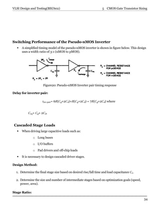
  • 34. 34 5 CMOS Gate Transistor Sizing VLSI Design and Testing(BEC602) Switching Performance of the Pseudo-nMOS Inverter  A simplified timing model of the pseudo-nMOS inverter is shown in figure below. This design uses a width ratio of 3:1 (nMOS to pMOS). Figure20: Pseudo-nMOS Inverter pair timing response Delay for inverter pair: tinv-pair= 6R(Cg+2Cd)+R(Cg+2Cd) = 7R(Cg+2Cd) where Ceq= Cg+ 2Cd. Cascaded Stage Loads  When driving large capacitive loads such as: o Long buses o I/O buffers o Pad drivers and off-chip loads  It is necessary to design cascaded driver stages. Design Method: 1. Determine the final stage size based on desired rise/fall time and load capacitance CL. 2. Determine the size and number of intermediate stages based on optimization goals (speed, power, area). Stage Ratio:
  • 35. 35 5 CMOS Gate Transistor Sizing VLSI Design and Testing(BEC602)  Defined as the ratio of transistor size between consecutive stages.  Optimal speed is obtained when the stage ratio is approximately 2.7.  Ratios between 2 and 10 are commonly used in practice.
  • 36. 36 6 Determination of Conductor Size VLSI Design and Testing (BEC602) 6 Determination of Conductor Size Electro migration  Electro migration refers to the movement of metal ions in a conductor due to the passage of direct current (DC).  This phenomenon results from the modification of normally random atomic diffusion to a directional process driven by the momentum transfer from electrons (charge carriers) to metal atoms. Effects of Electro migration:  Deformation of metal conductors  Creation of voids and hillocks  Potential failure of interconnects and circuitry Key Factors Affecting Electro migration:  Current density(J)  Temperature  Crystal structure of the metal Minimum Conductor Size Estimation  When designing power conductors, especially VDD and VSS lines, it is critical to keep the current density below threshold values to prevent electro migration-induced failures. Electro migration Threshold Example:  For a1µm thick aluminum line,the limiting current density is:  JAl≈1−2mA/µm  As a conservative design rule:  J≈0.5mA/µmto1.0 mA/µm  Should be used for power supply lines to avoid electro migration issues.
  • 37. 37 7 Power Consumption VLSI Design and Testing (BEC602) Current Crowding and Constrictions:  If a conductor has a constriction, metal atoms tend to migrate more rapidly in that region due to increased current density.  This leads to local weakening and eventual failure—similar to a fuse blowing. Voltage Drops(IRDrops)  Another reason for ensuring adequate conductor sizing is the voltage drop (IR drop) that can occur during charging transients.  These can cause improper functioning if VDD or VSS falls below critical limits. Note: Although electro migration typically sets the minimum width, IR drop considerations often determine the actual width required in practical design. Alternative Techniques for Power Distribution:  When increasing conductor width is not feasible: o Add extra VDD and VSS supply pins o Use multiple distributed power paths Current Density in Window Cuts  Special attention must be given to the current density at window (cut)edges.  It must be kept below:  Jcut≤0.1mA/µm  Due to current crowding effects near window peripheries, a chain of small, well-spaced windows can provide similar current carrying capability as one long narrow window.  This technique reduces peak current density and mitigates electro migration risk. 7 Power Consumption  In CMOS circuits, the total power dissipation arises from two primary components: 1. Static dissipation—due to leakage current 2. Dynamic dissipation—due to: o Switching transient currents o Charging and discharging of load capacitances
  • 38. 38 7 Power Consumption VLSI Design and Testing (BEC602) Static Dissipation  Consider a complementary CMOS gate as shown in figure below: Figure21:CMOS inverter states for static dissipation calculations  When the input is at logic ‘0’,then MOS is OFF and the pMOS is ON, pulling the output to VDD.  When the input is logic ‘1’, the nMOS is ON and the pMOS is OFF, pulling the output to ground (VSS).  In both states, one transistor is OFF, and there is no direct current path from VDD to VSS.  Hence, under ideal conditions, the quiescent current and power dissipation are zero.  However, there exists a small leakage current due to reverse-biased junctions between the diffusion regions and the substrate.  A model illustrating these parasitic diodes in a CMOS inverter is shown in figure below: Figure22:Model describing parasitic diodes
  • 39. 39 7 Power Consumption VLSI Design and Testing (BEC602) tp  The diode D1 models leakage from the p-well to substrate.  The reverse-biased leakage current is modeled by the diode equation: where: – is= reverse saturation current – V= voltage across the diode – q= electronic charge – k= Boltzmann’s constant – T= temperature (in Kelvin)  The static power dissipation is given by: Where n= number of devices  For example, typical static power dissipation due to leakage for an inverter operating at 5volts is between 1—2 nano-watts. Dynamic Dissipation  When the output switches states (either from ‘0’ to ‘1’ or ‘1’ to ‘0’), both nMOS and pMOS devices conduct for a brief interval.  This causes a short-duration current pulse from VDD to VSS.  Additionally, current is drawn to charge and discharge the load capacitance, which is typically the dominant component of dynamic power.  This short-circuit power dissipation is important in I/O buffer design and is influenced by gate design and capacitance.  Assuming a step input with rise/fall times much smaller than there petition period, the average dynamic power dissipation for a square-wave input with frequency fp=1 (as shown in figure below)is: where: – CL=load capacitance – VDD=supply voltage – fp=switching frequency
  • 40. 40 7 Power Consumption VLSI Design and Testing (BEC602) DD Pd=CLV2 fp  This equation shows that dynamic power is proportional to both the capacitance and the square of the supply voltage, and it increases linearly with frequency.  Note that it is independent of transistor parameters. Figure23: Waveforms for determination of dynamic power dissipation Total Power Dissipation  The total power consumed by a CMOS circuit is the sum of the static and dynamic components: Ptotal=Ps+Pd (4.41) Design Considerations  When estimating power dissipation:  Group all capacitances that operate at a given frequency.  Sum the contributions from each group to estimate total dynamic power.  Use the total dynamic power to size VDD and VSS conductors appropriately, minimizing IR drops.This consideration becomes increasingly important in large-scale CMOS designs.
  • 41. 41 8 Charge Sharing VLSI Design and Testing (BEC602) DD Example: Power Dissipation in CMOS Inverter Array Given: Number of inverters=N Operating frequency=10MHz VDD=+5V Output capacitance=2Cd, where Cd=40fF⇒2Cd= 80fF Input capacitance=2Cg,whereCg=11.2fF⇒2Cg=22.4fF Solution: Total capacitance per inverter: Ctotal=2Cd+2Cg=80fF+22.4fF=102.4fF Dynamic power per inverter: Pd=Ctotal·V2 ·fp=102.4×10−15 ·25·107 =2.56×10⁻⁵ W Total dynamic power for N inverters: Pd,total=N·2.56×10⁻⁵ W Static power (estimated leakage of 0.5nW per gate): Ps=N·0.5×10⁻⁹ W Total power: Ptotal≈ N·(2.56×10⁻⁵ +0.5×10⁻⁹ )W This example illustrates that dynamic power dominates static power in typical CMOS circuits. 8 Charge Sharing-In many digital CMOS circuits, especially during dynamic logic or bus operations, charge sharing is a critical consideration for maintaining signal integrity. Charge Sharing Model  A bus can be modeled as a capacitor Cb, as shown in figure below.Often, a signal from this bus is sampled via a switching element connected to another capacitor Cs. This configuration can be analyzed by modeling the pre-and post-switching charge conditions.
  • 42. 42 8 Charge Sharing VLSI Design and Testing (BEC602) R Figure24: Charge sharing mechanism Initial Conditions Before the switch is closed: Total initial charge: Total capacitance after switching: Qb= CbVb, Qs= CsVsQT= CbVb+ CsVs CT=Cb+Cs Final Voltage After Sharing  Once the switch closes, the charge redistributes, and both capacitors settle at a common voltage VR: V = QT = CbVb+CsVs Special Case: Vs≈0 CT Cb +Cs  Assuming Vb=VD D and Vs≈0, the resulting voltage becomes: VR=VDD Cb · Cb+Cs  This shows that VR is reduced compared to VDD, and the amount of drop depends on the ratio Cs/Cb. Design Guideline  To ensure reliable signal transfer from Cb to Cs, it is essential to maintain: Cb≥10·Cs  This minimizes the voltage drop due to charge sharing and preserves logic levels in sampling operations.
  • 43. 43 9 Scaling of MOS Transistor Sizing VLSI Design and Testing(BEC602) In digital circuits, sometimes we store voltage (like information)on a bus line, which acts like A big capacitor Cb. Another circuit part may want to sample that information using a smaller capacitor Cs through a switch (see the figure).This process is called charge sharing. Think of it like this: Cb is a big water tank with water level Vb, Cs is a small water tank with level Vs, A switch is like a valve that connects the two tanks. What happens when the valve is opened(switch closed)? Water (charge) flows between the tanks until both have the same level. The final level (voltage) is in between the original levels and depends on both volume (capacitance) and initial levels. Thefinalvoltagebecomes: VR= CbVb+CsVs C+C b s Special case: If Vb=VDD and Vs=0,then: V =V R DD · Cb C+C b s Problem: If Cs is too large, VR becomes much smaller than VDD, leading to unreliable logic levels. Design Tip: To avoid this, Cb>10·Cs This ensures the voltage remains close to the original bus value after sharing. Key Idea: Sharing charge is like mixing water. Keep the sampling tank small to avoid changing the level too much! Understanding Charge Sharing: A Simple Analogy 9 Scaling of MOS Transistor Sizing  As CMOS fabrication technology evolves, the dimensions of transistors are continually reduced to improve performance and increase packing density.  Let us examine how reducing device dimensions affects circuit behavior, guided by a first- order “constant-field” scaling model proposed by Dennardetal.
  • 44. 44 9 Scaling of MOS Transistor Sizing VLSI Design and Testing(BEC602) Scaling Principles  First-order MOS scaling theory assumes that the electric fields in the device are kept constant as dimensions are reduced.  If all critical parameters—such as device dimensions (length L, width W, oxide thickness tox, and junction depth Xj), voltages (VDD), and doping concentrations — are scaled by a factor α>1, then the key electrical properties of the device can still be preserved.  The scaling is applied as follows: – All horizontal and vertical dimensions are scaled by 1/α. – Voltages are scaled by 1/α. – Doping concentrations are scaled by α.  This approach results in a new device that is physically smaller, uses lower voltage, but maintains the same electric field intensities.  The outcome of such scaling is illustrated in figure and table shown below. Figure25: Basic scaled MOS device
  • 45. 45 9 Scaling of MOS Transistor Sizing VLSI Design and Testing(BEC602) Table8: Influence of First-Order Scaling on MOS Device Characteristics Parameter Scaling Factor Device Parameters Length L, Width W, Junction depth Xj Gate oxide thickness tox Substrate doping Na or Nd Supply voltage VDD Electric field E 1/α 1/α α 1/α 1(Constant) Depletion layer thickness d 1/α Parasitic capacitance C=WL/tox 1/α Gate delay(VC/I) 1/α Static power Ps, dynamic power Pd Power-speed product 1/α2 1/α3 Resultant Gate area A 1/α2 Influence Power density P/A 1(Constant) Current density I/A α Transconductance gm 1(Constant)  The primary benefit of constant-field scaling is that nonlinear effects are minimized, making design more predictable.  However, practical limits exist. For instance: – The depletion layer thickness d must reduce with L. – To reduced, we increase doping concentration, which affects mobility. – Electric fields remain constant, reducing the risk of breakdown.  One important rule is that the channel length must be larger than the sum of depletion widths from source and drain.  To scale L down, the depletion width must be reduced by increasing the substrate doping.  However, high doping reduces carrier mobility, increasing propagation delay.  Scaling also affects current and power: – Drain current Ids per transistor scales as 1/α. – Transistor density increases as α2 . – Current density increases as α. – Wider metal lines are needed to handle increased current. Power Density Consideration:  Though Pd per gate drops as 1/α2 , the number of gates increases as α2 , so overall power density remains constant.
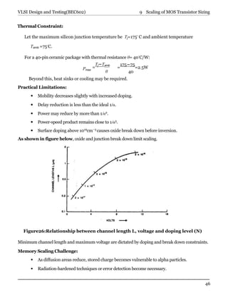
  • 46. 46 9 Scaling of MOS Transistor Sizing VLSI Design and Testing(BEC602) Thermal Constraint: Let the maximum silicon junction temperature be Tj=175◦ C and ambient temperature Tamb =75◦ C. For a 40-pin ceramic package with thermal resistance θ= 40◦ C/W: Pmax = Tj−Tamb θ = 175−75 =2.5W 40 Beyond this, heat sinks or cooling may be required. Practical Limitations:  Mobility decreases slightly with increased doping.  Delay reduction is less than the ideal 1/α.  Power may reduce by more than 1/α2 .  Power-speed product remains close to 1/α3 .  Surface doping above 1019 cm−3 causes oxide break down before inversion. As shown in figure below, oxide and junction break down limit scaling. Figure26:Relationship between channel length L, voltage and doping level (N) Minimum channel length and maximum voltage are dictated by doping and break down constraints. Memory Scaling Challenge:  As diffusion areas reduce, stored charge becomes vulnerable to alpha particles.  Radiation-hardened techniques or error detection become necessary.
  • 47. 47 9 Scaling of MOS Transistor Sizing VLSI Design and Testing(BEC602) Analogy Imagine squeezing a straw thinner and thinner, but not making it shorter. It becomes harder to blow through—not because it’s longer, but because it’s narrower. Similarly, when we scale down the width and thickness of metal interconnects (like squeezing the straw),but keep their length the same, their resistance increases significantly— just like the air resistance in the narrow straw. Interconnect Layer Scaling  While transistor performance improves with scaling, interconnect parameters degrade.  For example, scaling width and thickness of metal lines by 1/α reduces their cross-sectional area by 1/α2 .  The line resistance becomes: So, R scales as α2 . R′ =ρ l A′ l =ρ A/α2 =α2 R Note: The wire length is not scaled as some global wires (e.g. clock, power, long signal paths) still need to cross similar-sized chips because chip functionality grows.  If voltage is scaled down by 1/α, the voltage drop Vd along the interconnect (for constant chip size, i.e., unscaled l) increases by α.  Similarly, line response time becomes: τ′ =R′ C′ =α RC (for fixed interconnect length)  Hence, for constant chip size: – Voltage drops increase. – Response time worsens. – Signal integrity and clock distribution become harder. Table9: Influence of Scaling on Interconnect Media Parameter Scaling Factor Line resistance r α2 Line response rc α Normalized line response α Voltage drop Vd Normalized voltage drop α α Current density J α Normalized contact voltage drop α
  • 48. 48 10 Yield VLSI Design and Testing (BEC602) Key Issues: o Higher current density leads to electro migration. o New materials may be needed for metal layers. o Capacitance of interconnect increases. o Gates have less ability to drive long interconnects.  As shown in above table, the interconnection network becomes the bottleneck in performance. To mitigate this: o Vertical dimensions are often kept constant. o More metal layers are used. o Interconnect-aware design techniques are employed. 10 Yield  Yield is a critical factor in the manufacturing of VLSI (Very-Large-ScaleIntegration) circuits.  Although yield is not directly a performance parameter, it significantly affects the Economic feasibility of fabrication and is influenced by several factors: o Technology used in fabrication o Chip area o Layout strategy Definition of Yield: Yield is defined as: Yield (%)= No. of Good Chips on Wafer Total Number of Chips ×100% Yield depends primarily on the chip area (A) and the defect density (D) (number of lethal defects per cm2 ). Two widely accepted models describe how yield relates to these parameters. 1. Seed’s Yield Model: This model is used primarily when: o The chip area is large o The yield is expected to be less than 30% o The yield is expressed as:
  • 49. 49 10 Yield VLSI Design and Testing (BEC602) — where A = chip area (in cm2 ) D= defect density (lethal defects/cm2 )  As chip area increases or defect density rises, the exponent becomes more negative, causing yield to drop exponentially. 2. Murphy’s Yield Model: This model is preferred when:  Chip area is relatively small  Yield is expected to be greater than 30% o Murphy’s model gives:  This formulation softens the drastic yield drop for small areas, making it more accurate for high-yield conditions. Observations and Insights  Larger chip areas result in lower yield, due to the increased probability of a defect occurring anywhere in the chip.  In extreme cases, entire wafers can be rendered useless if the chip area is large and defect density is high.  Modern processes, such as dry etching, have improved defect densities. A typical value might be: Improving Yield D≈4defects/cm2  Redundancy can be built into chip designs, especially in memory circuits, to tolerate localized defects.  In random logic circuits, adding redundancy often increases chip area and may not improve yield significantly.  In contrast, memory arrays(which have a regular structure) can benefit greatly from techniques like spare rows or columns.