Embedded c programming guide e book atmel 8051 / 89c51 /89c52
13 likes8,987 views

The document appears to be a long string of repeating binary digits (010101010101...) with no other meaningful information. It consists entirely of binary numbers with no spaces or punctuation.


![RESEARCH DESIGN LABS | VOLUME 1, ISSUE 1 WWW.RESEARCHDESIGNLAB.COM
Program 3:
#include<reg51.h>
#define LCD_PORT P2
sbit rs=P3^5;
sbit en=P3^7;
sbit D7=P2^7;
sbit rw=P3^6;
sbit key1=P0^3;
sbit key2=P0^2;
sbit key3=P0^1;
sbit key4=P0^0;
void busy();
void CMD_WRT(unsigned char);
void LCD_WRT(unsigned char *);
void DATA_WRT(unsigned char);
void DELAY();
void main()
{
unsigned char CMD[]={0x38,0x0f,0x01,0x06,0x80};
unsigned char TEMP,i;
for(i=0;i<=4;i++)
{
TEMP=CMD[i];
CMD_WRT(TEMP);
}
CMD_WRT(0X01);
CMD_WRT(0X80);
LCD_WRT("RDL");
DELAY();
DELAY();
DELAY();
DELAY();
while(1)
{
//special function register declarations
//for the intended 8051 derivative
// LCD connections
//Define Port 2 as LCD Data pins.
//Register Select is connected to Port 3 pin 5
//Enable is connected to Port 3 pin 7
//Data Pin D7 is connected to Port 2 pin 7
//Read/Write is connected to Port 3 pin 6
// Keypad connections
//Switch 1 is connected to Port 0 pin 3
//Switch 2 is connected to Port 0 pin 2
//Switch 3 is connected to Port 0 pin 1
//Switch 4 is connected to Port 0 pin 0
// Call function declarations
//This Function checks whether the LCD is
//ready to receive next byte
//This Function is used to write commands
//into the LCD
//This Function is used to write Strings into
//the LCD
//This Function is used to write a byte of data
//into the LCD
//Call function declarations for delay
// MAIN CODE
// LCD Initialization
//commands, hex codes
// Variable declarations
//Write the commands into the LCD
//This command clears the LCD screen
//This moves the cursor to the beginning of the 1st
//line
//Writes the text 'RDL' in the LCD
//These delay's will hold the above text 'RDL' for
//some time
// Whatever comes next will execute forever
//Continuous loop](https://image.slidesharecdn.com/embeddedcprogrammingguidee-book-150911073955-lva1-app6891/85/Embedded-c-programming-guide-e-book-atmel-8051-89c51-89c52-21-320.jpg)


![RESEARCH DESIGN LABS | VOLUME 1, ISSUE 1 WWW.RESEARCHDESIGNLAB.COM
Program 4:
#include<reg52.h>
#define LCD_PORT P2
sbit rs=P3^5;
sbit en=P3^7;
sbit D7=P2^7;
sbit rw=P3^6;
sbit key1=P0^3;
sbit key2=P0^2;
sbit key3=P0^1;
sbit key4=P0^0;
sbit Relay1=P1^3;
sbit Relay2=P1^2;
sbit Relay3=P1^1;
sbit Relay4=P1^0;
void busy();
void CMD_WRT(unsigned char);
void LCD_WRT(unsigned char *);
void DATA_WRT(unsigned char);
void DELAY();
void main()
{
unsigned char CMD[]={0x38,0x0f,0x01,0x06,0x80};
unsigned char TEMP,i;
P1=0X00;
for(i=0;i<=4;i++)
{
TEMP=CMD[i];
CMD_WRT(TEMP);
}
//special function register declarations
//for the intended 8051 derivative
// LCD connections
//Define Port 2 as LCD Data pins.
//Register Select is connected
//to Port 3 pin 5
//Enable is connected
//to Port 3 pin 7
//Data Pin D7 is connected
//to Port 2 pin 7
//Read/Write is connected
//to Port 3 pin 6
// Keypad connections
//Switch 1 is connected to Port 0 pin 3
//Switch 2 is connected to Port 0 pin 2
//Switch 3 is connected to Port 0 pin 1
//Switch 4 is connected to Port 0 pin 0
// Relay Connections
//Relay 1 is connected to Port 1 pin 3
//Relay 2 is connected to Port 1 pin 2
//Relay 3 is connected to Port 1 pin 1
//Relay 4 is connected to Port 1 pin 0
// Call function declarations
//This Function checks whether the
//LCD is ready to receive next byte
//This Function is used to write commands
// into the LCD
//This Function is used to write Strings
//into the LCD
//This Function is used to write a byte
//of data into the LCD
//Call Function declarations for delay
// MAIN CODE
// LCD Initialization
// commands, hex codes
// Variable declarations
//Set Port 1 all bits to 0
//Write the commands into the LCD](https://image.slidesharecdn.com/embeddedcprogrammingguidee-book-150911073955-lva1-app6891/85/Embedded-c-programming-guide-e-book-atmel-8051-89c51-89c52-25-320.jpg)


![RESEARCH DESIGN LABS | VOLUME 1, ISSUE 1 WWW.RESEARCHDESIGNLAB.COM
Program 9:
#include"reg52.h"
#define CR 0X0D
#define LF 0X0A
#define EOM 0X1A
#define LCD_PORT P2
sbit rs=P3^5;
sbit rw=P3^6;
sbit en=P3^7;
sbit D7=P2^7;
void busy();
void CMD_WRT(unsigned char);
void LCD_WRT(unsigned char *);
void DATA_WRT(unsigned char);
void TRANSMIT(unsigned char *);
void transmit_byte(unsigned char );
void READ_SMS(void);
void SEND_CMD(unsigned char *BASE_ADD,unsigned char COUNT);
void SEND_CRLF(unsigned char);
unsigned char recv_byte (void);
void RX_REPLY();
void ENTER(void);
void DELAY();
unsigned char count12=0,message[50];
unsigned char byte1,k,temp;
unsigned char Test_Text[]="GSM Testing";
unsigned char code CMD_1[]="AT";
unsigned char code CMD_3[]="AT+CMGF=1";
unsigned char code CMD_4[]="AT+CMGD=1";
unsigned char code CMD_9[]="AT+CMGS="7411001407"";
//Special function register declarations
//for the intended 8051 derivative
//Define CR as 13
//Define LF as 10
//Define EOM as CNTRL+Z
// LCD connections
//Define Port 2 as LCD Data pins
//Register Select is connected to Port 3 pin 5
//Read/Write is connected to Port 3 pin 6
//Enable is connected to Port 3 pin 7
//Data Pin D7 is connected to Port 2 pin 7
// Call function declarations
//This Function checks whether the LCD is ready to
//receive next byte
//This Function is used to write commands
//into the LCD
//This Function is used to write Strings
//into the LCD
//This Function is used to write a byte of
//data into the LCD
//This Function is used to write Strings into
//the serial Port
//This Function is used to write a byte of
//data into the serial Port
//This function separates the text message from
//the SMS received
//This function sends GSM commands via the serial interface
//This function writes a 8 bit hex value into
//the serial interface
//This function receives a byte of data
//through the serial interface
//This function waits for a character 'K'(of OK) which
//the GSM modem replies for its commands
//This function is used to hit enter into the GSM
//modem whenever required
//Call Function declarations for delay
// Global variable declaration and initialization
// GSM commands declaration
//GSM Attention command
//GSM text initialization
//command
//Delete previous SMS
//command
//Edit the 10
//digit destination number here](https://image.slidesharecdn.com/embeddedcprogrammingguidee-book-150911073955-lva1-app6891/85/Embedded-c-programming-guide-e-book-atmel-8051-89c51-89c52-46-320.jpg)
![RESEARCH DESIGN LABS | VOLUME 1, ISSUE 1 WWW.RESEARCHDESIGNLAB.COM
void main()
{
unsigned char CMD[]={0x38,0x0f,0x01,0x06,0x80};
unsigned char I,TEMP,count=0;
for(i=0;i<=4;i++)
{
TEMP=CMD[i];
CMD_WRT(TEMP);
}
CMD_WRT(0X01);
CMD_WRT(0X80);
LCD_WRT(" RDL ");
DELAY();
DELAY();
DELAY();
CMD_WRT(0X01);
CMD_WRT(0X80);
LCD_WRT("Initializing GSM");
DELAY();
DELAY();
TMOD=0X20;
SCON=0X50;
TH1=0XFD;
TR1=1;
DELAY();
SEND_CMD(CMD_1,2);
DELAY();
ENTER();
RX_REPLY();
DELAY();
CMD_WRT(0X01);
CMD_WRT(0X80);
LCD_WRT("GSM Initialized!");
DELAY();
CMD_WRT(0XC0);
LCD_WRT("Sending SMS..");
DELAY();
// MAIN CODE
//LCD Initialization
//commands, hex codes
//Local variable declarations
//Initialization of LCD
//Write the commands into the LCD
//This command clears the LCD screen
//This moves the cursor to the beginning of the 1st line
//Writes the text 'RDL' in the LCD
//These delay's will hold the above text 'RDL' for some
//time on the LCD
//This command clears the LCD screen
//This moves the cursor to the beginning of the 1st line
//Writes the text 'Initializing GSM' in the LCD
//Serial Initialization
//Use Timer 1, mode 2
//Indicating serial mode 1, where an 8-bit data is
//framed with start and stop bits
//9600 baud rate
//Start timer
//Wait for some time for serial initialization to finish
//Enter GSM Attention command
//A small delay for relaxation
//Hit enter
//Wait for GSM modem to respond
//A small delay for relaxation
//This command clears the LCD screen
//This moves the cursor to the beginning of the 1st line
//Writes the text 'GSM Initialized ' in the LCD
//A small delay for relaxation
//This moves the cursor to the beginning of the
//2nd line
//Writes the text 'Sending SMS..' from the
//current pointer of LCD
//A small delay for relaxation](https://image.slidesharecdn.com/embeddedcprogrammingguidee-book-150911073955-lva1-app6891/85/Embedded-c-programming-guide-e-book-atmel-8051-89c51-89c52-47-320.jpg)


![RESEARCH DESIGN LABS | VOLUME 1, ISSUE 1 WWW.RESEARCHDESIGNLAB.COM
// Function used to transmit a string of data into the serial interface
//execute the next statement till the end of the string
//Pass the 8 bit data located at the address location
// of the pointer to the function 'transmit_byte'
//Function used for sending an 8 bit data present on the variable
// 'byte' to the serial interface
//Move the contents of the variable 'byte' to serial buffer memory
//Wait until TI flag is set by hardware when an entire byte has
//been transmitted
//Forcibly clear TI flag
//This function waits until a SMS has been received and separates the text
//message from it and displays it on the LCD
//GSM read SMS command
//Local Variables declaration and initialization
//Assign any value to byte other than '+'
//Breaks this loop only when '+' has been received, till then
//the variable 'byte' keeps waiting for '+' to be received
//Keep checking for the data received in the
//call function 'recv_byte'
//A small delay for relaxation
//A small delay for relaxation
//Enter the command used for reading a SMS
//Hit enter
//The string that comes next includes quotes(") along with other
//information like time, date, number etc. of the received SMS
//Wait for at least 8 such quotes(")
//Breaks this loop only when '"' has been received, till then
//the variable 'byte' keeps waiting for '"' to be received
//Keep checking for the data received in the call
//function 'recv_byte'
//Assign any value to byte other than '"'
//Assign any value to byte other than '13'
//Breaks this loop only when '13' has been received, till then
//the variable 'byte' keeps waiting for '13' to be received
//Keep checking for the data recieved in the
//call function 'recv_byte'
void TRANSMIT(unsigned char *string)
{
while(*string)
transmit_byte(*string++);
}
void transmit_byte(unsigned char byte)
{
SBUF=byte;
while(!TI);
TI=0;
}
void READ_SMS(void)
{
unsigned char code CMD_5[]="AT+CMGR=1";
unsigned char byte,i=0, flag=0;
byte=0;
while(byte!='+')
{
byte=recv_byte();
}
DELAY();
DELAY();
SEND_CMD(CMD_5,9);
ENTER();
for(i=0;i<7;i++)
{
while(byte!='"')
{
byte=recv_byte();
}
byte=0;
}
byte=0;
while(byte!=13)
{
byte=recv_byte();
}](https://image.slidesharecdn.com/embeddedcprogrammingguidee-book-150911073955-lva1-app6891/85/Embedded-c-programming-guide-e-book-atmel-8051-89c51-89c52-51-320.jpg)
![RESEARCH DESIGN LABS | VOLUME 1, ISSUE 1 WWW.RESEARCHDESIGNLAB.COM
byte=0;
count12=0;
while(byte!=13)
{
byte=recv_byte();
message[count12]= byte;
count12++;
}
count12--;
CMD_WRT(0X01);
CMD_WRT(0X80);
DELAY();
for (k=1;k<count12;k++)
{
temp=message[k];
DATA_WRT(temp);
DELAY();
}
count12=0;
DELAY();
SEND_CMD(CMD_4,9);
DELAY();
ENTER();
RX_REPLY();
DELAY();
}
unsigned char recv_byte()
{
unsigned char D;
while(RI!=1);
D = SBUF;
RI=0;
return(D);
}
//Assign any value to byte other than '13'
//Initialize the text character counter to zero
//Breaks this loop only when '13' has been received, till then
//the variable 'byte' keeps waiting for '13' to be received
//Keep checking for the data received in the
//call function 'recv_byte'
//Move the received byte of data into the
//array 'message'
//Increment the array
//Decrement the text character counter by 1 to
//eliminate the last value received i.e '13'
//This command clears the LCD screen
//This moves the cursor to the beginning of the 1st line
//A small delay for relaxation
//Separate out individual characters of the message
//string to variable 'temp'
//Display the individual characters on the LCD 1 by 1
//A small delay for relaxation
//Clear the text character counter back to zero.
//A small delay for relaxation
//Enter Delete previous SMS command to free up
//space for new SMS
//A small delay for relaxation
//Hit enter
//Wait for GSM modem to respond
//A small delay for relaxation
//This function receives a byte of data through the serial interface
//and returns
//it back to the function where it was called
//Local variable declaration
//Wait until RI flag is set by hardware when an
//entire byte has been received
//Move the received byte of data into variable 'D'
//Forcibly clear RI flag
//Return the value to the called function where it was called](https://image.slidesharecdn.com/embeddedcprogrammingguidee-book-150911073955-lva1-app6891/85/Embedded-c-programming-guide-e-book-atmel-8051-89c51-89c52-52-320.jpg)


![RESEARCH DESIGN LABS | VOLUME 1, ISSUE 1 WWW.RESEARCHDESIGNLAB.COM
sbit rd=P3^0;
sbit wr=P3^1;
sbit intr=P3^3;
void read();
void conv();
unsigned int adc_value;
void main()
{
unsigned char CMD[]={0x38,0x0f,0x01,0x06,0x80};
unsigned char i,TEMP;
for(i=0;i<=4;i++)
{
TEMP=CMD[i];
CMD_WRT(TEMP);
}
CMD_WRT(0X01);
CMD_WRT(0X80);
LCD_WRT("ADC0804..RDL. ");
while(1)
{
CMD_WRT(0XC4);
conv();
read();
CONVERT_DISPLAY(adc_value);
DELAY();
DELAY();
DELAY();
}
}
void DELAY()
{
unsigned int X=60000;
while(X--);
//RD of ADC0804 IC is connected to Port 3 pin 0
//WR of ADC0804 IC is connected to Port 3 pin 1
//INTR of ADC0804 IC is connected to Port 3 pin 3
//LCD Initialization commands, hex codes
//Local variable declarations
//Initialization of lcd
//Write the commands into the LCD
//This command clears the LCD screen
//This moves the cursor to the beginning of the 1st line
//Writes the text 'ADC0804..RDL.' in the LCD
//cursor on second line
// call conv to convert anolog voltage to digtal 8 bit
// call read toi read 8 bit digtal value
//convert and display
//Function for delay routine
// larger the value of X and Y the more is the delay.
// executes this statement until X decrements to 0;](https://image.slidesharecdn.com/embeddedcprogrammingguidee-book-150911073955-lva1-app6891/85/Embedded-c-programming-guide-e-book-atmel-8051-89c51-89c52-55-320.jpg)

![RESEARCH DESIGN LABS | VOLUME 1, ISSUE 1 WWW.RESEARCHDESIGNLAB.COM
//This Function is used to convert Hex data to Decimal equivalent
//and write into the LCD
//Local variable declarations
//Local variable declarations
//Local variable declarations
//Move the Hex value 'd' to a variable 'temp'
//Get the last number
//Get the 2nd last number
//Get the first number
//Concatenate all the value into a single variable
//or'ing with 0x30 will give
//the ASCII equivalent of the decimal value
//Write the 8 bit data into the LCD
//Make WR low
//nop delay
//Make WR high
//Wait for INTR to go low
//Make RD low
//Read ADC port
//Make RD high
void CONVERT_DISPLAY(unsigned char d)
{
unsigned char dig1,dig2,dig3,dig[3];
unsigned char x;
unsigned char temp;
temp=d;
temp=temp/10;
dig1=d%10;
dig2=temp%10;
dig3=temp/10;
dig[0]=dig3;
dig[1]=dig2;
dig[2]=dig1;
CMD_WRT(0XCA);
for(x=0;x<3;x++)
{
temp=dig[x]|0x30;
DATA_WRT(temp);
}
}
void conv() {
wr = 0;
_nop_ ();
_nop_ ();
_nop_ ();
wr = 1;
while (intr);
}
void read() {
rd = 0;
_nop_ ();
_nop_ ();
_nop_ ();
adc_value = adc_port;
rd = 1;
}](https://image.slidesharecdn.com/embeddedcprogrammingguidee-book-150911073955-lva1-app6891/85/Embedded-c-programming-guide-e-book-atmel-8051-89c51-89c52-57-320.jpg)


More Related Content
What's hot (20)
Similar to Embedded c programming guide e book atmel 8051 / 89c51 /89c52 (20)


More from Raghav Shetty (20)


Recently uploaded (20)


Embedded c programming guide e book atmel 8051 / 89c51 /89c52
- 2. RESEARCH DESIGN LABS | VOLUME 1, ISSUE 1 WWW.RESEARCHDESIGNLAB.COM Embedded Systems 8051/89S52 Microcontroller Introduction The 8051 microcontroller is one of the most popular general purpose microcontrollers in use today. The 8051 is an 8-bit microcontroller which means that most available operations are limited to 8 bits. 8051 chips are used in a wide variety of control systems, telecom applications, robotics as well as in the automotive industry. There are 4 8-bit ports: P0, P1, P2 and P3. PORT P1 (Pins 1 to 8): The port P1 is a general purpose input/output port which can be used for a variety of interfacing tasks. The other ports P0, P2 and P3 have dual roles or additional functions associated with them based upon the context of their usage. The port 1 output buffers can sink/source four TTL inputs. When 1s are written to portn1 pins are pulled high by the internal pull-ups and can be used as inputs. Fig A. Pin description of 8051 PORT P3 (Pins 10 to 17): PORT P3 acts as a normal IO port, but Port P3 has additional functions such as, serial transmit and receive pins, 2 external interrupt pins, 2 external counter inputs, read and write pins for memory access. PORT P2 (pins 21 to 28): PORT P2 can also be used as a general purpose 8 bit port when no external memory is present, but if external memory access is required then PORT P2 will act as an address bus in conjunction with PORT P0 to access external memory. PORT P2 acts asA8-A15, as can be seen from fig 1.1 PORT P0 (pins 32 to 39)P0 can be used as a general purpose 8 bit port when no external memory is present, but if external memory access is required then PORT P0 acts as a multiplexed address and data bus that can be used to access external memory in conjunction with PORT P2. P0 acts as AD0- AD7, as can be seen from fig 1.1 Overview: Ports:
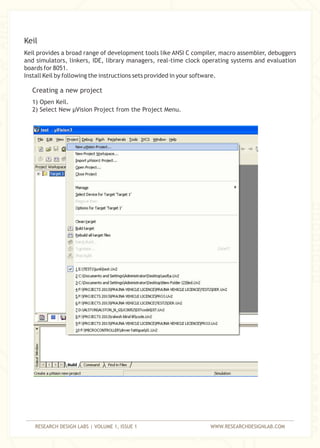
- 3. RESEARCH DESIGN LABS | VOLUME 1, ISSUE 1 WWW.RESEARCHDESIGNLAB.COM Keil provides a broad range of development tools like ANSI C compiler, macro assembler, debuggers and simulators, linkers, IDE, library managers, real-time clock operating systems and evaluation boards for 8051. Install Keil by following the instructions sets provided in your software. 1) Open Keil. 2) Select New µVision Project from the Project Menu. Keil Creating a new project
- 4. RESEARCH DESIGN LABS | VOLUME 1, ISSUE 1 WWW.RESEARCHDESIGNLAB.COM 3) Name the project ‘Led1’. 4) Click on the Save Button. 5) The device window will be displayed. Select the manufacturer of the IC. Here let us use ATMEL AT89S52 6) Double Click on Atmel. Tips IR Obstacle Sensor Quick Overview Based on a simple basic Idea, this IR obstacle sensor, is easy to build, easy to calibrate and still, it provides a detection range of 10- 30 cm. This sensor can be used for most indoor applications where no important ambient light is present. It is the same principle in ALL Infra- Red proximity sensors. The basic idea is to send infra red light through IR-LEDs, which is then reflected by any object in front of the sensor. Code & Schematic For more details www.researchdesignlab.com
- 5. RESEARCH DESIGN LABS | VOLUME 1, ISSUE 1 WWW.RESEARCHDESIGNLAB.COM 7) Scroll down and select AT89S52 8) Click OK 9) Choose No. Tips Carbon Monoxide Sensor Quick Overview M Q - 7 g a s s e n s o r composed by micro AL2O3 ceramic tube, Tin Dioxide (SnO2) sensitive layer , measuring electrode and heater are fixed into a crust made by plastic and stainless steel net. The h e a t e r p r o v i d e s n e c e s s a r y w o r k conditions for work of sensitive components. Code & Schematic For more details www.researchdesignlab.com
- 6. RESEARCH DESIGN LABS | VOLUME 1, ISSUE 1 WWW.RESEARCHDESIGNLAB.COM Creating a new source file 1)Click File Menu and select New. 2) A new window will open up in the Keil IDE. 3) Let us write a simple code that would toggle the status of Port 1 with a small delay.
- 7. RESEARCH DESIGN LABS | VOLUME 1, ISSUE 1 WWW.RESEARCHDESIGNLAB.COM 4) Click on File menu and select Save as… 5) Name the file Led1_blinking.c 6) Click the Save Button 7) In the ‘Project Workspace’ window, click on the ‘+’ symbol in front of Target1. Tips Quick Overview This is a simple-to-use liquefied petroleum gas (LPG) sensor, suitable for sensing LPG (composed of mostly propane and butane) concentrations in the air. Used in gas leakage detecting equipments for detecting of LPG, iso-butane, propane, LNG combustible gases. If output goes above a preset range the output is low else high in idle condition. Code & Schematic For more details www.researchdesignlab.com Gas Sensor
- 8. RESEARCH DESIGN LABS | VOLUME 1, ISSUE 1 WWW.RESEARCHDESIGNLAB.COM 8) Below that ‘Source Group 1’ would appear, right click on it. 9) Click on “Add Files to Group ‘Source Group 1’ ” 10) Select ‘Led1_blinking.c’ 11) Click Add button 12) Click Close button. Tips Digital Soil Moisture Sensor Quick Overview This sensor can be used to test the moisture of soil, when the soil is having water shortage, the module output is at high level, else the output is at low level. By using this sensor one can automatically water the flower plant, or any other plants requiring automatic watering technique. Module triple output mode, digital output is simple, analog output more accurate, serial output with exact readings.
- 9. RESEARCH DESIGN LABS | VOLUME 1, ISSUE 1 WWW.RESEARCHDESIGNLAB.COM 13) Click Close button. Expand the Source Group 1 in the tree menu to ensure that the file was added to the project. Tips Code & Schematic For more details www.researchdesignlab.com Digital Heart Beat Sensor Quick Overview This heart beat sensor is designed to give digital output of heart beat when a finger is placed on it. When the heartbeat detector is working, the top-most LED flashes with each heart beat. This digital output can be connected to micro controller directly to measure the Beats Per Minute (BPM) rate. It works on the principle of light modulation by blood flow through finger at each pulse. Module dual output mode, digital output is simple, serial output with exact readings.
- 10. RESEARCH DESIGN LABS | VOLUME 1, ISSUE 1 WWW.RESEARCHDESIGNLAB.COM Creating HEX for the Part 1) Right click on Target 1 in Tree menu 2) Select Options for Target ‘Target 1’ 3) Select Target Tab 4) Change Xtal (Mhz) from 33.0 to 11.0592 Tips Analog Light Intensity Sensor Quick Overview Light dependent resistor (LDR), suitable for use in projects which require a device or circuit to be automatically switched on or off in darkness or light. As the amount of light falling on this LDR increases, its resistance decreases. The light detector itself is just 5mm in diameter.Analog output more accurate. Code & Schematic For more details www.researchdesignlab.com
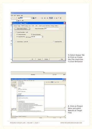
- 11. RESEARCH DESIGN LABS | VOLUME 1, ISSUE 1 WWW.RESEARCHDESIGNLAB.COM 5) Select Output Tab 6) Click on Create Hex File check box 7) Click OK Button 8. Click on Project Menu and select Rebuild all Target Files
- 12. RESEARCH DESIGN LABS | VOLUME 1, ISSUE 1 WWW.RESEARCHDESIGNLAB.COM 9. In the Build Window it should report ‘0 Errors (s), 0 Warnings’ 10. You are now ready to Program your Part Tips Code & Schematic For more details www.researchdesignlab.com Digital Vibration Sensor Quick Overview This basic piezo sensor can be used in anti-theft devices, electronic locks, mechanical equipment vibration detection, sound gesture application and detection range bull's-eye counts vibration testing occasions. These vibration levels could be given to any controller/processor and necessary decisions could be taken through it. Module triple output mode, digital output is simple, analog output more accurate, serial output with exact readings.
- 13. RESEARCH DESIGN LABS | VOLUME 1, ISSUE 1 WWW.RESEARCHDESIGNLAB.COM Testing Program in Debugger 1) Click on the File Menu and select Save 2)Click on Project Menu and select Rebuild all Target Files Tips Digital Light Intensity Sensor Quick Overview Light dependent resistor (LDR), suitable for use in projects which require a device or circuit to be automatically switched on or off in darkness or light. As the amount of light falling on this LDR increases, its resistance decreases. The light detector itself is just 5mm in diameter. Module triple output mode, digital output is simple, analog output more accurate, serial output with exact readings. Code & Schematic For more details www.researchdesignlab.com
- 14. RESEARCH DESIGN LABS | VOLUME 1, ISSUE 1 WWW.RESEARCHDESIGNLAB.COM 3) In the Build Window it should report ‘0 Errors (s), 0 Warnings’ 4) Click on Debug Menu and Select Start/Stop Debug Session. 5) If you are using a free version of Keil the dialog appears. Click OK. Tips Serial Ultrasonic Distance Measure Quick Overview Ultrasonic Distance Sensor comes with an ASCII serial O/P and provided optimum ranging & detection of long to short distance ranges. Owing to their stable, precise, non- contact and accurate distance measurements from about 2 cm to 4 m e t e r s . C o m p a c t l y designed, easy usable, high ranging and easily interfaced upon micro controllers RX and TX pin. Code & Schematic For more details www.researchdesignlab.com
- 15. RESEARCH DESIGN LABS | VOLUME 1, ISSUE 1 WWW.RESEARCHDESIGNLAB.COM Running the Keil Debugger (Simulation) 1) The Keil Debugger should be now running. 2) Click on Peripherals. Select I/O Ports, Select Port 1. Tips Ultrasonic Ranging Sensor Quick Overview U l t r a s o n i c s e n s o r provides stable and a c c u r a t e d i s t a n c e measurements from 2cm to 450cm. It has an focus of less than 15 degrees and an accuracy of about 2mm. Code & Schematic For more details www.researchdesignlab.com
- 16. RESEARCH DESIGN LABS | VOLUME 1, ISSUE 1 WWW.RESEARCHDESIGNLAB.COM 3) A new window should port will pop up. This represents the Port and Pins 4) To execute your code Click ‘Run’. The Parallel Port 1 Box status should change as a continuous loop. Tips Ultrasonic Obstacle Sensor Quick Overview Used to detect the move of human or object. Suitable for indoor and outdoor burglar proof application, vehicle a p p l i c a t i o n , AT M survillence camera etc. Code & Schematic For more details www.researchdesignlab.com
- 17. RESEARCH DESIGN LABS | VOLUME 1, ISSUE 1 WWW.RESEARCHDESIGNLAB.COM 5) To exit out, first Click on Debug Menu and Select Stop Running 6) And then Click on Debug Menu and Select Start/Stop Debug Session Tips Gyro Sensor Quick Overview The L3G4200DTR is a low-power, three-axis angular rate sensor, able t o p r o v i d e u n p r e c e d e n t e d stablility of zero rate level and sensitivity over temperature and time.It includes a sensing element and an IC interface capable of providing the measured angular rate to the external world through a d i g i t a l i n t e r f a c e (I2C/SPI). Code & Schematic For more details www.researchdesignlab.com
- 18. RESEARCH DESIGN LABS | VOLUME 1, ISSUE 1 WWW.RESEARCHDESIGNLAB.COM Learn embedded C programming in 8051 Circuit and Working: Fig.1 shows the circuit of simple 8051 Microcontroller interfaced with LED’s. Here are 3 simple programs for controlling LED’s through simple Embedded C programming in Microcontroller. Program 1 shows how to control the entire port by toggling 8 LED’s. Program 2 shows how to control single I/O pin of the controller one by one just like a Decimal counter output. Testing: 1) Write the program as shown below and generate the ‘hex’ file by the instructions provided in chapter 1. 2) Burn the code with the help of burner to the controller. 3) Power ON your microcontroller and check the result as per your program. Components/modules required : 1) 8051 project board (assembled/non assembled kit). 2) 5V DC source. 3) 8 LED’s. 4) Resistors (1KΩx8). 5) IC AT89S52. 6) 8051 IC burner. 7) Connectors and cables. Fig 1. Circuit Diagram for LCD and 1x4 keypad interfacing LED Blinking using 8051 Microcontroller and Keil – AT89S52
- 19. RESEARCH DESIGN LABS | VOLUME 1, ISSUE 1 WWW.RESEARCHDESIGNLAB.COM Program 1: #include<reg52.h> #define LEDPORT P2 void delay(); void main() { P2=0X00; while(1) { LEDPORT =0XFF; delay(); LEDPORT =0X00; delay(); } } void delay() { unsigned int x=60000; while (x--) ; } // special function register //declarations for the // intended 8051 derivative //Defining Port 2 as the //'LEDPORT' // Function prototype declaration //Main Code //Set Port 2 all bits to 0 //infinite loop //Set LEDPORT all bits to 1 // Wait for a small delay //Set LEDPORT all bits to 0 // Wait for small delay // Delay Routine // larger the value of x //the more is the delay. // executes this statement // until x decrements to 0 Program 2: #include<reg52.h> void delay(); sbit LED0=P2^0; sbit LED1=P2^1; sbit LED2=P2^2; sbit LED3=P2^3; sbit LED4=P2^4; sbit LED5=P2^5; sbit LED6=P2^6; sbit LED7=P2^7; void main()//Main Code { P1=0x00; while(1) { LED0=1; delay(); LED1=1; delay(); //special function register declarations //for the intended 8051 derivative // Function prototype declaration //Define Port Pin P2.0 as LED0 //Define Port Pin P2.1 as LED1 //Define Port Pin P2.2 as LED2 //Define Port Pin P2.3 as LED3 //Define Port Pin P2.4 as LED4 //Define Port Pin P2.5 as LED5 //Define Port Pin P2.6 as LED6 //Define Port Pin P2.7 as LED7 //Set Port 2 all bits to 0 // Continuous loop //Turn ON LED0 //Wait for a small delay //Turn ON LED1 //Wait for a small delay Tips Current Sensor 20A Quick Overview The ACS712 provides economical and precise solutions for AC or DC current sensing in industrial, commercial, and communications systems. The device package allows for easy implementation by the c u s t o m e r. Ty p i c a l applications include motor control, load d e t e c t i o n a n d m a n a g e m e n t , switchmode power s u p p l i e s , a n d o v e r c u r r e n t f a u l t protection. The device is not intended for a u t o m o t i v e applications. Code & Schematic For more details www.researchdesignlab.com
- 20. RESEARCH DESIGN LABS | VOLUME 1, ISSUE 1 WWW.RESEARCHDESIGNLAB.COM LED2=1; delay(); LED3=1; delay(); LED4=1; delay(); LED5=1; delay(); LED6=1; delay(); LED7=1; delay(); P1=0x00; delay(); } } void delay() { unsigned int x=60000 while (x--); } //Turn ON LED2 //Wait for a small delay //Turn ON LED3 //Wait for a small delay //Turn ON LED4 //Wait for a small delay //Turn ON LED5 //Wait for a small delay //Turn ON LED6 //Wait for a small delay //Turn ON LED7 //Wait for a small delay //Turn OFF all LED's //Wait for a small delay // Delay Routine // larger the value of x the //more is the delay. // executes this statement //until x decrements to 0 LCD Keypad interfacing using 8051 Microcontroller and Keil– AT89S52 Circuit and Working: Components/modules required: Fig.2 shows the circuit of simple 8051 Microcontroller interfaced with LCD and 1x4 Keypad. Here is a simple program for interfacing LCD and keypad through simple Embedded C programming in Microcontroller. Program 3 demonstrates how to display in a LCD when an event occurs like a key is being pressed. 1) 8051 project board (assembled/non assembled kit). 2) 5V DC source. 3) LCD interfacing Module 4) 4 Keys keypad 5) IC AT89S52. 6) 8051 IC burner. 7) Connectors and cables. Fig 2. Circuit Diagram for LCD and 1x4 keypad interfacing
- 21. RESEARCH DESIGN LABS | VOLUME 1, ISSUE 1 WWW.RESEARCHDESIGNLAB.COM Program 3: #include<reg51.h> #define LCD_PORT P2 sbit rs=P3^5; sbit en=P3^7; sbit D7=P2^7; sbit rw=P3^6; sbit key1=P0^3; sbit key2=P0^2; sbit key3=P0^1; sbit key4=P0^0; void busy(); void CMD_WRT(unsigned char); void LCD_WRT(unsigned char *); void DATA_WRT(unsigned char); void DELAY(); void main() { unsigned char CMD[]={0x38,0x0f,0x01,0x06,0x80}; unsigned char TEMP,i; for(i=0;i<=4;i++) { TEMP=CMD[i]; CMD_WRT(TEMP); } CMD_WRT(0X01); CMD_WRT(0X80); LCD_WRT("RDL"); DELAY(); DELAY(); DELAY(); DELAY(); while(1) { //special function register declarations //for the intended 8051 derivative // LCD connections //Define Port 2 as LCD Data pins. //Register Select is connected to Port 3 pin 5 //Enable is connected to Port 3 pin 7 //Data Pin D7 is connected to Port 2 pin 7 //Read/Write is connected to Port 3 pin 6 // Keypad connections //Switch 1 is connected to Port 0 pin 3 //Switch 2 is connected to Port 0 pin 2 //Switch 3 is connected to Port 0 pin 1 //Switch 4 is connected to Port 0 pin 0 // Call function declarations //This Function checks whether the LCD is //ready to receive next byte //This Function is used to write commands //into the LCD //This Function is used to write Strings into //the LCD //This Function is used to write a byte of data //into the LCD //Call function declarations for delay // MAIN CODE // LCD Initialization //commands, hex codes // Variable declarations //Write the commands into the LCD //This command clears the LCD screen //This moves the cursor to the beginning of the 1st //line //Writes the text 'RDL' in the LCD //These delay's will hold the above text 'RDL' for //some time // Whatever comes next will execute forever //Continuous loop
- 22. RESEARCH DESIGN LABS | VOLUME 1, ISSUE 1 WWW.RESEARCHDESIGNLAB.COM if (key1 ==0) { CMD_WRT(0X01); CMD_WRT(0X80); LCD_WRT("Key 1 is pressed"); while(key1==0); } else if (key2 ==0) { CMD_WRT(0X01); CMD_WRT(0X80); LCD_WRT("Key 2 is pressed"); while(key2==0); } else if (key3 ==0) CMD_WRT(0X01); CMD_WRT(0X80); LCD_WRT("Key 3 is pressed"); while(key3==0); } else if (key4 ==0) { CMD_WRT(0X01); CMD_WRT(0X80); LCD_WRT("Key 4 is pressed"); while(key4==0); } else { CMD_WRT(0X01); CMD_WRT(0X80); LCD_WRT("No key Pressed"); DELAY(); DELAY(); DELAY(); } } } void busy() { D7=1; rs=0; rw=1; //Check whether switch 1 is being pressed //Clears the LCD screen //Moves the cursor to the beginning of the 1st line //Writes the text within quotes in the LCD //Wait until the switch has been released //Check whether switch 2 is being pressed //Clears the LCD screen //Moves the cursor to the beginning of the 1st line //Writes the text within quotes in the LCD //Wait until the switch has been released //Check whether switch 3 is being pressed { //Clears the LCD screen //Moves the cursor to the beginning of the 1st line //Writes the text within quotes in the LCD //Wait until the switch has been released //Check whether switch 4 is being pressed //Clears the LCD screen //Moves the cursor to the beginning of the 1st line //Writes the text within quotes in the LCD //Wait until the switch has been released //Clears the LCD screen //Moves the cursor to the beginning of the 1st line //Writes the text within quotes in the LCD // A small delay for relaxation //This Function checks whether the LCD is ready to receive next byte //Keep D7 pin to High //Keep RS to Low to select command register //RW=1 for read
- 23. RESEARCH DESIGN LABS | VOLUME 1, ISSUE 1 WWW.RESEARCHDESIGNLAB.COM while(D7!=0) { en=0; en=1; } } void CMD_WRT(unsigned char val) { busy(); LCD_PORT=val; rs=0; rw=0; en=1; en=0; } void LCD_WRT(unsigned char *string) { while(*string) DATA_WRT(*string++); } void DATA_WRT(unsigned char ch) { busy(); LCD_PORT = ch; rs=1; rw=0; en=1; en=0; } void DELAY() { unsigned int X=60000,Y=60000; while(X--); while(Y--); } //Monitor D7 pin until it gets low //Provide a latch pulse from low to high to EN //This Function is used to write commands into the LCD //Execute busy function to know whether the LCD is //ready to receive any data/command //Put the variable val into LCD_PORT which is //connected to LCD data pins //Keep RS to Low to select command register // RW=0 for write //Provide a latch pulse from High to Low to EN //This Function is used to write Strings into the LCD //increment from the beginning of the string until a //null character is detected (end of the string) //separates a single byte from the string //This Function is used to write a byte of data into the LCD //Execute busy function to know whether the LCD is //ready to receive any data/command //Put the variable ch into LCD_PORT which is //connected to LCD data pins //Keep RS to High to select Data register // RW=0 for write //Provide a latch pulse from High to Low to EN //function for delay routine // larger the value of X and Y the more is the //delay. //executes this statement until X decrements to 0 //executes this statement until Y decrements to 0
- 24. RESEARCH DESIGN LABS | VOLUME 1, ISSUE 1 WWW.RESEARCHDESIGNLAB.COM LCD Keypad and Relays interfacing using 8051 Microcontroller and Keil–AT89S52 Circuit and Working: Fig.3.1 and Fig.3.2 shows the circuit of simple 8051 Microcontroller interfaced with LCD, 1x4 Keypad and 4 Relays. Here is a simple Embedded C program for interfacing 4 Relays to a 8051 Microcontroller which could be controlled by a key press event through a 1x4 keypad, the result or state of the relays being displayed on the LCD interfaced along with this. Program 4 enables a user to toggle the state of relays by pressing a key consequently the result gets displayed on the LCD interfaced. Fig 3.2. Circuit Diagram for Relay LCD and 1x4 keypad interfacing - Part 2. Fig 3.1. Circuit Diagram for Relay LCD and 1x4 keypad interfacing - Part 1. Components/modules required: 1) 8051 project board (assembled/non assembled kit). 2) 12V and 5V DC source. 3) LCD interfacing Module 4) 4 Keys keypad 5) 4 Relay Interfacing Board 12V 6) IC AT89S52. 7) 8051 IC burner. 8) Connectors and cables
- 25. RESEARCH DESIGN LABS | VOLUME 1, ISSUE 1 WWW.RESEARCHDESIGNLAB.COM Program 4: #include<reg52.h> #define LCD_PORT P2 sbit rs=P3^5; sbit en=P3^7; sbit D7=P2^7; sbit rw=P3^6; sbit key1=P0^3; sbit key2=P0^2; sbit key3=P0^1; sbit key4=P0^0; sbit Relay1=P1^3; sbit Relay2=P1^2; sbit Relay3=P1^1; sbit Relay4=P1^0; void busy(); void CMD_WRT(unsigned char); void LCD_WRT(unsigned char *); void DATA_WRT(unsigned char); void DELAY(); void main() { unsigned char CMD[]={0x38,0x0f,0x01,0x06,0x80}; unsigned char TEMP,i; P1=0X00; for(i=0;i<=4;i++) { TEMP=CMD[i]; CMD_WRT(TEMP); } //special function register declarations //for the intended 8051 derivative // LCD connections //Define Port 2 as LCD Data pins. //Register Select is connected //to Port 3 pin 5 //Enable is connected //to Port 3 pin 7 //Data Pin D7 is connected //to Port 2 pin 7 //Read/Write is connected //to Port 3 pin 6 // Keypad connections //Switch 1 is connected to Port 0 pin 3 //Switch 2 is connected to Port 0 pin 2 //Switch 3 is connected to Port 0 pin 1 //Switch 4 is connected to Port 0 pin 0 // Relay Connections //Relay 1 is connected to Port 1 pin 3 //Relay 2 is connected to Port 1 pin 2 //Relay 3 is connected to Port 1 pin 1 //Relay 4 is connected to Port 1 pin 0 // Call function declarations //This Function checks whether the //LCD is ready to receive next byte //This Function is used to write commands // into the LCD //This Function is used to write Strings //into the LCD //This Function is used to write a byte //of data into the LCD //Call Function declarations for delay // MAIN CODE // LCD Initialization // commands, hex codes // Variable declarations //Set Port 1 all bits to 0 //Write the commands into the LCD
- 26. RESEARCH DESIGN LABS | VOLUME 1, ISSUE 1 WWW.RESEARCHDESIGNLAB.COM CMD_WRT(0X01); CMD_WRT(0X80); LCD_WRT("RDL"); DELAY(); DELAY(); DELAY(); DELAY(); while(1) { if (key1 ==0 && Relay1==0) { CMD_WRT(0X01); CMD_WRT(0X80); LCD_WRT("Relay 1 is ON"); Relay1=1; while(key1==0); } else if (key1 ==0 && Relay1==1) { CMD_WRT(0X01); CMD_WRT(0X80); LCD_WRT("Relay 1 is OFF"); Relay1=0; while(key1==0); } else if (key2 ==0 && Relay2==0) { CMD_WRT(0X01); CMD_WRT(0X80); LCD_WRT("Relay 2 is ON"); Relay2=1; while(key2==0); } else if (key2 ==0 && Relay2==1) { CMD_WRT(0X01); CMD_WRT(0X80); LCD_WRT("Relay 2 is OFF"); Relay2=0; while(key2==0); } else if (key3 ==0 && Relay3==0) { CMD_WRT(0X01); CMD_WRT(0X80); LCD_WRT("Relay 3 is ON"); Relay3=1; while(key3==0); } //This command clears the LCD screen //This moves the cursor to the beginning of the 1st line //Writes the text 'RDL' in the LCD //These delay's will hold the above text 'RDL' for some time //Continuous loop //Check whether switch 1 is being pressed //and Relay1 is OFF //Clears the LCD screen //Moves the cursor to the beginning of the 1st line //Writes the text within quotes in the LCD //Turn ON Relay1 //Wait until the switch has been released //Check whether switch 1 is being pressed //and Relay1 is ON //Clears the LCD screen //Moves the cursor to the beginning of the 1st line //Writes the text within quotes in the LCD //Turn OFF Relay1 //Wait until the switch has been released //Check whether switch 2 is being pressed //and Relay2 is OFF //Clears the LCD screen //Moves the cursor to the beginning of the 1st line //Writes the text within quotes in the LCD //Turn ON Relay2 //Wait until the switch has been released //Check whether switch 2 is being pressed //and Relay2 is ON //Clears the LCD screen //Moves the cursor to the beginning of the 1st line //Writes the text within quotes in the LCD //Turn OFF Relay2 //Wait until the switch has been released //Check whether switch 3 is being pressed //and Relay3 is OFF //Clears the LCD screen //Moves the cursor to the beginning of the 1st line //Writes the text within quotes in the LCD //Turn ON Relay3 //Wait until the switch has been released
- 27. RESEARCH DESIGN LABS | VOLUME 1, ISSUE 1 WWW.RESEARCHDESIGNLAB.COM else if (key3 ==0 && Relay3==1) { CMD_WRT(0X01); CMD_WRT(0X80); LCD_WRT("Relay 3 is OFF"); Relay3=0; while(key3==0); } else if (key4 ==0 && Relay4==0) { CMD_WRT(0X01); CMD_WRT(0X80); LCD_WRT("Relay 4 is ON"); Relay4=1; while(key4==0); } else if (key4 ==0 && Relay4==1) { CMD_WRT(0X01); CMD_WRT(0X80); LCD_WRT("Relay 4 is OFF"); Relay4=0; while(key4==0); else { CMD_WRT(0X01); CMD_WRT(0X80); LCD_WRT("Press any key.."); DELAY(); } } } void busy() { D7=1; rs=0; rw=1; while(D7!=0) { en=0; en=1; } } //Check whether switch 3 is being pressed //and Relay3 is ON //Clears the LCD screen //Moves the cursor to the beginning of the 1st line //Writes the text within quotes in the LCD //Turn OFF Relay3 //Wait until the switch has been released //Check whether switch 4 is being pressed //and Relay4 is OFF //Clears the LCD screen //Moves the cursor to the beginning of the 1st line //Writes the text within quotes in the LCD //Turn ON Relay4 //Wait until the switch has been released //Check whether switch 4 is being pressed //and Relay4 is ON //Clears the LCD screen //Moves the cursor to the beginning of the 1st line //Writes the text within quotes in the LCD //Turn OFF Relay4 //Wait until the switch has been released } //Clears the LCD screen //Moves the cursor to the beginning of the 1st line //Writes the text within quotes in the LCD // A small delay for relaxation //This Function checks whether the LCD is ready to receive //next byte //Keep D7 pin to High //Keep RS to Low to select command register // RW=1 for read //Monitor D7 pin until it gets low //Provide a latch pulse from low to high to EN
- 28. RESEARCH DESIGN LABS | VOLUME 1, ISSUE 1 WWW.RESEARCHDESIGNLAB.COM void CMD_WRT(unsigned char val) { busy(); LCD_PORT=val; rs=0; rw=0; en=1; en=0; } void LCD_WRT(unsigned char *string) { while(*string) DATA_WRT(*string++); } void DATA_WRT(unsigned char ch) { busy(); LCD_PORT = ch; rs=1; rw=0; en=1; en=0; } void DELAY() { unsigned int X=60000; while(X--); } //This Function is used to write commands into the LCD //Execute busy function to know whether the LCD is //ready to receive any data/command //Put the variable val into LCD_PORT which is //connected to LCD data pins //Keep RS to Low to select command register // RW=0 for write //Provide a latch pulse from High to Low to EN //This Function is used to write Strings into the LCD // increment from the beginning of the string until //a null character is detected (end of the string) //separates a single byte from the string //This Function is used to write a byte of data into the LCD //Execute busy function to know whether the LCD //is ready to receive any data/command //Put the variable ch into LCD_PORT which is //connected to LCD data pins //Keep RS to High to select Data register // RW=0 for write //Provide a latch pulse from High to Low to EN //Function for delay routine // larger the value of X the more is the delay. //executes this statement until X decrements to 0
- 29. RESEARCH DESIGN LABS | VOLUME 1, ISSUE 1 WWW.RESEARCHDESIGNLAB.COM Asynchronous serial data communication is widely used for character-oriented transmissions. Each character is placed in between start and stop bits, this is called framing. Block-oriented data transfers use the synchronous method. The start bit is always one bit, but the stop bit can be one or two bits. The start bit is always a 0 (low) and the stop bit(s) is 1 (high). We need a line driver (voltage converter) to convert the R232’s signals to TTL voltage levels that will be acceptable to 8051’s TxD and RxD pins. The baud rate of 8051 system should match the baud rate of the PC’s COM port. Serial Communication Fig 4.1 Rs232 to TTL Conversion Fig 4.2 Serial Transmission of Character ‘A’
- 30. RESEARCH DESIGN LABS | VOLUME 1, ISSUE 1 WWW.RESEARCHDESIGNLAB.COM SM0, SM1 They determine the framing of data by specifying the number of bits per character, and the start and stop bits. REN (receive enable) It is a bit-addressable register When it is high, it allows 8051 to receive data on RxD pin If low, and should be picked up before data is framed with start andthe receiver is disable. it is lost. stop bits. 4. TR1 is set to 1 to start timer 1TI (transmit interrupt) Programming the 8051 to 5. TI is cleared by (TI=0;) TIWhen 8051 finishes the transfer transfer character bytes instructionof 8-bit Character It raises TI serially. 6. The character byte to beflag to indicate that it is ready 1. TMOD register is loaded with transferred serially is writtento transfer another byte TI bit the value TMOD=0X20, into SBUF registeris raised at the beginning of the indicating the use of timer 1 in 7. The TI flag bit is monitoredstop bit mode 2 (8-bit auto-reload) to with the use of instruction set baud rate. while (TI==0); to see if theRI (receive interrupt) 2. The TH1 is loaded with one of c h a r a c t e r h a s b e e nWhen 8051 receives data the values to set baud rate for transferred completely.serially via RxD, it gets rid of the serial data transfer 8. To transfer the next byte, gostart and stop bits and places 3. The SCON register is loaded to step 5the byte in SBUF register It with the value 50H, indicatingraises the RI flag bit to indicate serial mode 1, where an 8-bitthat a byte has been received Programming the 8051 to receive character bytes serially 1. TMOD register is loaded with the value TMOD=0X20, indicating the use of timer 1 in mode2 (8-bit auto-reload) to set baud rate 2. TH1 is loaded to set baud rate 3. The SCON register is loaded with the value SCON=0X50,indicating serial mode 1, where an 8- bit data is framed with start and stop bits 4. TR1 is set to 1 to start timer 1 5. RI is cleared by RI=0; RI instruction 6. The RI flag bit is monitored with the use of instruction while(RI==0); to see if an entire character has been received yet. 7. When RI is raised, SBUF has the byte, its contents are moved into a safe place 8. To receive the next character, go to step 5 Fig 4.3: Serial Mode Selector
- 31. RESEARCH DESIGN LABS | VOLUME 1, ISSUE 1 WWW.RESEARCHDESIGNLAB.COM Simple Serial interfacing using 8051 Microcontroller and Keil– AT89S52 Circuit and Working: Fig.5 shows the circuit of simple 8051 Microcontroller interfaced with LED’s. Here is a simple Embedded C program for interfacing 8 LED’s to a 8051 Microcontroller which could be turned ON or OFF by sending few serial commands. Program 5 enables a user to turn ON/OFF a series of LED’s by sending serial data. The program is designed in such a way that a serial command A1 will turn ON the first LED and A0 will turn of the same LED. Similarly B1 will turn ON the second LED and B0 will turn of the same LED. This will continue for the remaining 6 LED’s. i.e. H1 and H0 would turn ON and OFF last LED (8th LED) respectively. You can enter the inputs in any serial window monitor software like Hyperterminal, Putty etc. Also you could design a GUI in software like Matlab, .NET etc. which could be used to control these LED’s. Components/modules required : 1) 8051 project board with RS232 interface (assembled/non assembled kit). 2) 5V DC source. 3) 8 LED’s. 4) Resistors (1KΩx8). 5) IC AT89S52. 6) 8051 IC burner. 7) Connectors and cables. Fig. 5 Circuit Diagram for Serial and LED interfacing
- 32. RESEARCH DESIGN LABS | VOLUME 1, ISSUE 1 WWW.RESEARCHDESIGNLAB.COM #include<reg52.h> void delay(); sbit LED0=P2^0; sbit LED1=P2^1; sbit LED2=P2^2; sbit LED3=P2^3; sbit LED4=P2^4; sbit LED5=P2^5; sbit LED6=P2^6; sbit LED7=P2^7; unsigned char byte1,byte2; void main() { TMOD=0X20; SCON=0X50; TH1=0XFD; TR1=1; delay(); TI=0; SBUF='S'; while (TI==0); TI=0; delay(); P2=0x00; while(1) { RI=0; while(RI==0); byte1=SBUF; RI=0; while(RI==0); byte2=SBUF; RI=0; delay(); delay(); if(byte1=='A') { if(byte2=='1') { //special function register declarations //for the intended 8051 derivative // Function prototype declaration //Define Port Pin P2.0 as LED0 //Define Port Pin P2.1 as LED1 //Define Port Pin P2.2 as LED2 //Define Port Pin P2.3 as LED3 //Define Port Pin P2.4 as LED4 //Define Port Pin P2.5 as LED5 //Define Port Pin P2.6 as LED6 //Define Port Pin P2.7 as LED7 // Variable declarations // MAIN CODE //Serial Initialization //use Timer 1, mode 2 //indicating serial mode 1, where an 8-bit //data is framed with start and stop bits //9600 baud rate //Start timer //Wait for a delay for serial initialization to finish // Transmit 'S' to check whether the setup is ready //Forcibly change the Transmit Interrupt Flag of 8051 to 0 //Move 'S' to serial buffer memory //Wait until TI flag is set by hardware when an entire byte //has been transmitted // Forcibly clear TI flag //A small delay for relaxation //Set Port 2 all bits to 0 // continuous loop //Forcibly clear the Receive Interrupt Flag of 8051 to 0 //Wait until RI flag is set by hardware when an entire byte //has been received //Move the received byte of data into variable 'byte1' //Forcibly clear RI flag //Wait until RI flag is set by hardware when an entire byte //has been received //Move the received byte of data into variable 'byte2' //Forcibly clear RI flag //Check whether the 1st byte of //data is 'A' //Check whether the 2nd byte of //data is '1'
- 33. RESEARCH DESIGN LABS | VOLUME 1, ISSUE 1 WWW.RESEARCHDESIGNLAB.COM LED0=1; delay(); } else if(byte2=='0') { LED0=0; delay(); } } else if(byte1=='B') { if(byte2=='1') { LED1=1; delay(); } else if(byte2=='0') { LED1=0; delay(); } } else if(byte1=='C') { if(byte2=='1') { LED2=1; delay(); } else if(byte2=='0') { LED2=0; delay(); } } else if(byte1=='D') { if(byte2=='1') { LED3=1; } //Turn ON LED0 //Wait for a small delay //Check whether the 2nd byte of //data is '0' //Turn OFF LED0 //Wait for a small delay //Check whether the 1st byte of //data is 'B' //Check whether the 2nd byte of //data is '1' //Turn ON LED1 //Wait for a small delay //Check whether the 2nd byte of //data is '0' //Turn OFF LED1 //Wait for a small delay //Check whether the 1st byte of //data is 'C' //Check whether the 2nd byte of //data is '1' //Turn ON LED2 //Wait for a small delay //Check whether the 2nd byte of //data is '0' //Turn OFF LED2 //Wait for a small delay //Check whether the 1st byte of //data is 'D' //Check whether the 2nd byte of //data is '1' //Turn ON LED3 Tips SOIC to DIP Adapter 8-Pin Quick Overview Adapter for standard 8 SOIC SMD Parts to convert to standard 8 Pin DIP size.This SOIC breakout board is a PCB which will interface an SOIC package to 0.1" (2.54mm) headers which c a n b e u s e d o n b r e a d b o a r d s f o r p r o t o t y p i n g y o u r projects.Simply solder- on your 8-pin SOIC form- factor IC, along with some 0.1-inch-pitch headers, and you will h a v e a u s a b l e , breadboard-friendly unit. Code & Schematic For more details www.researchdesignlab.com
- 34. RESEARCH DESIGN LABS | VOLUME 1, ISSUE 1 WWW.RESEARCHDESIGNLAB.COM delay(); } else if(byte2=='0') { LED3=0; delay(); } } else if(byte1=='E') { if(byte2=='1') { LED4=1; delay(); } else if(byte2=='0') { LED4=0; delay(); } } else if(byte1=='F') { if(byte2=='1') { LED5=1; delay(); } else if(byte2=='0') { LED5=0; delay(); } } else if(byte1=='G') { if(byte2=='1') { LED6=1; delay(); } else if(byte2=='0') { LED6=0; delay(); } } else if(byte1=='H') { //Wait for a small delay //Check whether the 2nd byte of //data is '0' //Turn OFF LED3 //Wait for a small delay //Check whether the 1st byte of //data is 'E' //Check whether the 2nd byte of //data is '1' //Turn ON LED4 //Wait for a small delay //Check whether the 2nd byte of //data is '0' //Turn OFF LED4 //Wait for a small delay //Check whether the 1st byte of //data is 'F' //Check whether the 2nd byte of //data is '1’ //Turn ON LED5 //Wait for a small delay //Check whether the 2nd byte of //data is '0' //Turn OFF LED5 //Wait for a small delay //Check whether the 1st byte of //data is 'G' //Check whether the 2nd byte of //data is '1' //Turn ON LED6 //Wait for a small delay //Check whether the 2nd byte of //data is '0' //Turn OFF LED6 //Wait for a small delay //Check whether the 1st byte of //data is 'H' Tips Current Sensor 05A Code & Schematic For more details www.researchdesignlab.com Quick Overview The ACS712 provides economical and precise solutions for AC or DC current sensing in industrial, commercial, and communications systems. The device package allows foreasy implementation by the c u s t o m e r. Ty p i c a l applicationsinclude motor control, load d e t e c t i o n a n d m a n a g e m e n t , switchmode power s u p p l i e s , a n d o v e r c u r r e n t f a u l t protection. The device is not intended for a u t o m o t i v e applications.
- 35. RESEARCH DESIGN LABS | VOLUME 1, ISSUE 1 WWW.RESEARCHDESIGNLAB.COM if(byte2=='1') { LED7=1; delay(); } else if(byte2=='0') { LED7=0; delay(); } } else { P2=0x00; delay(); } } } void delay() { unsigned int x=60000; while (x--); } //Check whether the 2nd byte of //data is '1' //Turn ON LED7 //Wait for a small delay //Check whether the 2nd byte of //data is '0' //Turn OFF LED7 //Wait for a small delay //Set Port 2 all bits to 0 if any //other variable has been received //Wait for a small delay // Delay Routine // larger the value of x //the more is the delay. // executes this statement //until x decrements to 0 Bluetooth and Relays interfacing using 8051 Microcontroller and Keil– AT89S52 Circuit and Working: Fig.6 shows the circuit of simple 8051 Microcontroller interfaced with Bluetooth and 4 relays. Program 6 demonstrates how to receive data through Bluetooth. Components/modules required : 1) 8051 project board (assembled/non assembled kit). 2) 5V and 12V DC source. 3) Bluetooth Module. 4) 12V 4 Relay board. 5) IC AT89S52. 6) 8051 IC burner. 7) Connectors and cables. Fig .6 Circuit Diagram for Bluetooth and 4 Relay interfacing
- 36. RESEARCH DESIGN LABS | VOLUME 1, ISSUE 1 WWW.RESEARCHDESIGNLAB.COM Program 6: #include<reg52.h> void delay(); sbit Relay1=P2^3; sbit Relay2=P2^2; sbit Relay3=P2^1; sbit Relay4=P2^0; unsigned char byte1,byte2; void main() { TMOD=0X20; SCON=0X50; TH1=0XFD; TR1=1; delay(); TI=0; SBUF='S'; while (TI==0); TI=0; delay(); P2=0x00; while(1) { RI=0; while(RI==0); byte1=SBUF; ' RI=0; while(RI==0); byte2=SBUF; RI=0; if(byte1=='1') { if(byte2=='N') { Relay1=1; } //special function register declarations //for the intended 8051 derivative //Function prototype declaration // Relay Connections //Relay 1 is connected to Port 2 pin 3 //Relay 2 is connected to Port 2 pin 2 //Relay 3 is connected to Port 2 pin 1 //Relay 4 is connected to Port 2 pin 0 // Variable declarations // MAIN CODE //Serial Initialization //use Timer 1, mode 2 //indicating serial mode 1,where an 8-bit data //is framed with start and stop bits //9600 baud rate //Start timer //Wait for some time for serial initialization to finish // Transmit 'S' to check whether the setup is ready //Forcibly change the Transmit //Interrupt Flag of 8051 to 0 //Move 'S' to serial buffer memory //Wait until TI flag is set by hardware //when an entire byte has been transmitted // Forcibly clear TI flag //A small delay for relaxation //Set Port 2 all bits to 0 // continuous loop //Forcibly clear the Receive //Interrupt Flag of 8051 to 0 //Wait until RI flag is set by hardware //when an entire byte has been received //Move the received byte of data into variable 'byte1 //Forcibly clear RI flag //Wait until RI flag is set by hardware //when an entire byte has been received //Move the received byte of data into variable 'byte2' //Forcibly clear RI flag //Check whether the 1st byte of data is '1' //Check whether the 2nd byte of data is 'N' //Turn ON Relay1
- 37. RESEARCH DESIGN LABS | VOLUME 1, ISSUE 1 WWW.RESEARCHDESIGNLAB.COM else if(byte2=='F') { Relay1=0; } } else if(byte1=='2') { if(byte2=='N') { Relay2=1; } else if(byte2=='F') { Relay2=0; } } else if(byte1=='3') { if(byte2=='N') { Relay3=1; } else if(byte2=='F') { Relay3=0; } } else if(byte1=='4') if(byte2=='N') { Relay4=1; } else if(byte2=='F') { Relay4=0; } } else if(byte1=='X') { if(byte2=='N') { P2=0xFF; } else if(byte2=='F') { P2=0x00; } } //Check whether the 2nd byte of data is 'F' //Turn OFF Relay1 //Check whether the 1st byte of data is '2' //Check whether the 2nd byte of data is 'N' //Turn ON Relay2 //Check whether the 2nd byte of data is 'F' //Turn OFF Relay2 //Check whether the 1st byte of data is '3' //Check whether the 2nd byte of data is 'N' //Turn ON Relay3 //Check whether the 2nd byte of data is 'F' //Turn OFF Relay3 //Check whether the 1st byte of data is '4' { //Check whether the 2nd byte of data is 'N' //Turn ON Relay4 //Check whether the 2nd byte of data is 'F' //Turn OFF Relay4 //Check whether the 1st byte of data is 'X' //Check whether the 2nd byte of data is 'N' //Turn ON all the Relays //Check whether the 2nd byte of data is 'F' //Turn OFF all the Relays
- 38. RESEARCH DESIGN LABS | VOLUME 1, ISSUE 1 WWW.RESEARCHDESIGNLAB.COM else { P2=0x00; } } } void delay() { unsigned int x=60000; while (x--); } //Clear Port 2 all bits to 0 if any other variable has been received //Function for delay routine //Delay Routine // larger the value of x the more is the delay. // executes this statement until x decrements to 0 Fig.7 shows the circuit of simple 8051 Microcontroller interfaced with XBee and 1x4 Keypad. Program 7 demonstrates how to send data wirelessly when a key is being pressed. Components/modules required : 1) 8051 project board (assembled/non assembled kit). 2) 5V DC source. 3) XBee(S2) 4) XBee power supply board 5) 1X4 keys keypad. 6) IC AT89S52. 7) 8051 IC burner. 8) Connectors and cables. Fig 7. Circuit Diagram for LCD and 1x4 keypad interfacing Keypad and XBee interfacing using 8051 Microcontroller and Keil– AT89S52 Circuit and Working:
- 39. RESEARCH DESIGN LABS | VOLUME 1, ISSUE 1 WWW.RESEARCHDESIGNLAB.COM Program 7: #include<reg51.h> sbit key1=P0^3; sbit key2=P0^2; sbit key3=P0^1; sbit key4=P0^0; void DELAY(); void main() { unsigned char flag1=0,flag2=0,flag3=0,flag4=0; //Variable declarations TMOD=0X20; SCON=0X50; TH1=0XFD; TR1=1; DELAY(); TI=0; SBUF='S'; while (TI==0); TI=0; DELAY(); P1=0X00; DELAY(); while(1) { if (key1 ==0 && flag1==0) { SBUF='A'; while (TI==0); TI=0; flag1=1; while(key1==0); DELAY(); } else if (key1 ==0 && flag1==1) { SBUF='B'; while (TI==0); TI=0; flag1=0; while(key1==0); DELAY(); } //special function register declarations //for the intended 8051 derivative // Keypad connections //Switch 1 is connected to Port 0 pin 3 //Switch 2 is connected to Port 0 pin 2 //Switch 3 is connected to Port 0 pin 1 //Switch 4 is connected to Port 0 pin 0 //Call Function declarations for delay //Serial Initialization //use Timer 1, mode 2 //indicating serial mode 1, where an 8-bit data is //framed with start and stop bits //9600 baud rate //Start timer //Wait for a delay for serial initialization to finish // Transmit 'S' to check whether the setup is ready //Forcibly clear the Transmit Interrupt Flag of 8051 to 0 //Move 'S' to serial buffer memory //Wait until TI flag is set by hardware when an //entire byte has been transmitted //Forcibly clear TI flag //A small delay for relaxation //Set Port 1 all bits to 0 //Continuous loop //Check whether switch 1 is being pressed //flag1 is Low //Move 'A' to serial buffer memory //Wait until TI flag is set by hardware when an //entire byte has been transmitted // Forcibly clear TI flag //Set flag1 //Wait until the switch has been released //A small delay for relaxation //Check whether switch 1 is being pressed //and flag1 is Low //Move 'B' to serial buffer memory //Wait until TI flag is set by hardware when an //entire byte has been transmitted // Forcibly clear TI flag //Clear flag1 //Wait until the switch has been released //A small delay for relaxation
- 40. RESEARCH DESIGN LABS | VOLUME 1, ISSUE 1 WWW.RESEARCHDESIGNLAB.COM else if (key2 ==0 && flag2==0) { SBUF='C'; while (TI==0); TI=0; flag2=1; while(key2==0); DELAY(); } else if (key2 ==0 && flag2==1) { SBUF='D'; while (TI==0); TI=0; flag2=0; while(key2==0); DELAY(); } else if (key3 ==0 && flag3==0) { SBUF='E'; while (TI==0); TI=0; flag3=1; while(key3==0); DELAY(); } else if (key3 ==0 && flag3==1) { SBUF='F'; while (TI==0); TI=0; flag3=0; while(key3==0); DELAY(); } else if (key4 ==0 && flag4==0) { SBUF='G'; while (TI==0); //Check whether switch 2 is being pressed //and flag2 is Low //Move 'C' to serial buffer memory //Wait until TI flag is set by hardware //when an entire byte has been transmitted //Forcibly clear TI flag //Set flag2 //Wait until the switch has been released //A small delay for relaxation //Check whether switch 2 is being pressed //and flag2 is High //Move 'D' to serial buffer memory //Wait until TI flag is set by hardware //when an entire byte has been transmitted //Forcibly clear TI flag //Clear flag2 //Wait until the switch has been released //A small delay for relaxation //Check whether switch 3 is being pressed //and flag3 is Low //Move 'E' to serial buffer memory //Wait until TI flag is set by hardware //when an entire byte has been transmitted //Forcibly clear TI flag //Set flag3 //Wait until the switch has been released //A small delay for relaxation //Check whether switch 3 is being pressed //and flag3 is High //Move 'F' to serial buffer memory //Wait until TI flag is set by hardware //when an entire byte has been transmitted // Forcibly clear TI flag //Clear flag3 //Wait until the switch has been released //A small delay for relaxation //Check whether switch 4 is being pressed //and flag4 is Low //Move 'G' to serial buffer memory //Wait until TI flag is set by hardware //when an entire byte has been transmitted
- 41. RESEARCH DESIGN LABS | VOLUME 1, ISSUE 1 WWW.RESEARCHDESIGNLAB.COM TI=0; flag4=1; while(key4==0); DELAY(); } else if (key4 ==0 && flag4==1) { SBUF='H'; while (TI==0); TI=0; flag4=0; while(key4==0); DELAY(); } } } void DELAY() { unsigned int X=60000; while(X--); } // Forcibly clear TI flag //Set flag4 //Wait until the switch has been released //A small delay for relaxation //Check whether switch 4 is being pressed //and flag4 is High //Move 'H' to serial buffer memory //Wait until TI flag is set by hardware //when an entire byte has been transmitted // Forcibly clear TI flag //Clear flag4 //Wait until the switch has been released //A small delay for relaxation //Function for delay routine // larger the value of X the more is the delay. // executes this statement until / X decrements to 0 3 Axis Accelerometer Quick Overview 3-axis accelerometer to now have an on-board 3.3V regulator - making it a perfect choice for interfacing with a 5V microcontroller such as the . This breakout comes with 3 analog outputs for X, Y and Z axis breakout board. The ADXL335 is the latest and greatest from Analog Devices, known for their exceptional quality MEMS devices. The VCC takes up to 5V in and regulates it to 3.3V with an output pin. The analog outputs are ratiometric: that means that 0g measurement output is always at half of the 3.3V output (1.65V), -3g is at 0v and 3g is at 3.3V with full scaling in between. Fully assembled and tested. The XYZ filter capacitors are 0.1uF for a 50 Hz bandwidth Tips Code & Schematic For more details www.researchdesignlab.com
- 42. RESEARCH DESIGN LABS | VOLUME 1, ISSUE 1 WWW.RESEARCHDESIGNLAB.COM LED’s and XBee interfacing using 8051 Microcontroller and Keil– AT89S52 Circuit and Working: Fig.8 shows the circuit of simple 8051 Microcontroller interfaced with XBee and 8 LED’s. Program 8 demonstrates how to receive serial data wirelessly and toggle the state of a LED. Components/modules required : 1) 8051 project board (assembled/non assembled kit). 2) 5V DC source. 3) XBee(S2) 4) XBee power supply board 5) 8 LED’s. 6) Resistors (1KΩx8). 7) IC AT89S52. 8) 8051 IC burner. 9) Connectors and cables. Fig. 8 Circuit Diagram for XBee and LED interfacing
- 43. RESEARCH DESIGN LABS | VOLUME 1, ISSUE 1 WWW.RESEARCHDESIGNLAB.COM Program 8: #include<reg52.h> void delay(); sbit LED0=P2^0; sbit LED1=P2^1; sbit LED2=P2^2; sbit LED3=P2^3; sbit LED4=P2^4; sbit LED5=P2^5; sbit LED6=P2^6; sbit LED7=P2^7; unsigned char byte1,byte2; void main() { TMOD=0X20; SCON=0X50; TH1=0XFD; TR1=1; delay(); TI=0; SBUF='S'; while (TI==0); TI=0; delay(); P2=0x00; while(1) { RI=0; while(RI==0); byte1=SBUF; RI=0; if(byte1=='A') { LED0=1; LED4=1; } else if(byte1=='B') //special function register declarations //for the intended 8051 derivative // Function prototype declaration //Define Port Pin P2.0 as LED0 //Define Port Pin P2.1 as LED1 //Define Port Pin P2.2 as LED2 //Define Port Pin P2.3 as LED3 //Define Port Pin P2.4 as LED4 //Define Port Pin P2.5 as LED5 //Define Port Pin P2.6 as LED6 //Define Port Pin P2.7 as LED7 // Variable declarations // MAIN CODE //Serial Initialization //use Timer 1, mode 2 //indicating serial mode 1, where an 8-bit //data is framed with start and stop bits //9600 baud rate //Start timer //Wait for some time for serial initialization to finish // Transmit 'S' to check whether the setup is ready //Forcibly change the Transmit Interrupt //Flag of 8051 to 0 //Move 'S' to serial buffer memory //Wait until TI flag is set by hardware //when an entire byte has been transmitted // Forcibly clear TI flag //A small delay for relaxation //Set Port 2 all bits to 0 // continuous loop //Forcibly clear the Receive Interrupt //Flag of 8051 to 0 //Wait until RI flag is set by hardware //when an entire byte has been received //Move the received byte of data into variable 'byte1' //Forcibly clear RI flag //Check whether the received byte of data is 'A' //Turn on LED0 //Turn on LED4 //Check whether the received byte of data is 'B'
- 44. RESEARCH DESIGN LABS | VOLUME 1, ISSUE 1 WWW.RESEARCHDESIGNLAB.COM { LED0=0; LED4=0; } else if(byte1=='C') { LED1=1; LED5=1; } else if(byte1=='D') { LED1=0; LED5=0; } else if(byte1=='E') { LED2=1; LED6=1; } else if(byte1=='F') { LED2=0; LED6=0; } else if(byte1=='G') { LED3=1; LED7=1; } else if(byte1=='H') LED3=0; LED7=0; } else { P2=0x00; delay(); } } } void delay() { unsigned int x=60000; while (x--); } //Turn off LED0 //Turn off LED4 //Check whether the received byte of data is 'C' //Turn on LED1 //Turn on LED5 //Check whether the received byte of data is 'D' //Turn off LED1 //Turn off LED5 //Check whether the received byte of data is 'E' //Turn on LED2 //Turn on LED6 //Check whether the received byte of data is 'F' //Turn off LED2 //Turn off LED6 //Check whether the received byte of data is 'G' //Turn on LED3 //Turn on LED7 //Check whether the received byte of data is 'H' { //Turn off LED3 //Turn off LED7 //Set Port 2 all bits to 0 //if any other variable has been received //Wait for a small delay // Delay Routine // larger the value of x the more is the delay. // executes this statement until x decrements to 0
- 45. RESEARCH DESIGN LABS | VOLUME 1, ISSUE 1 WWW.RESEARCHDESIGNLAB.COM GSM Modem and LCD interfacing using 8051 Microcontroller and Keil– AT89S52 Circuit and Working: Fig.9 shows the circuit of simple 8051 Microcontroller interfaced with GSM Modem and LCD. The Modem sends an SMS every time you turn on your microcontroller. Following this the modem will be waiting for any message to be received, once a message has been received, the message will be displayed on the LCD. Program 9 demonstrates how to initialize GSM modem through “AT” commands via a serial interface and send/receive a SMS through it. Please note: GSM modem needs to be turned on at least 10 seconds before you turn on the micro controller (GSM takes a few seconds to turn on) Fig.9 Circuit Diagram for GSM Modem and 16X2 LCD Components/modules required : 1)8051 project board (assembled/non assembled kit). 2)5V and 12V,1A DC source. 3)GSM Module. 4)16X2 LCD interfacing module. 5)IC AT89S52. 6)8051 IC burner. 7)Connectors and cables.
- 46. RESEARCH DESIGN LABS | VOLUME 1, ISSUE 1 WWW.RESEARCHDESIGNLAB.COM Program 9: #include"reg52.h" #define CR 0X0D #define LF 0X0A #define EOM 0X1A #define LCD_PORT P2 sbit rs=P3^5; sbit rw=P3^6; sbit en=P3^7; sbit D7=P2^7; void busy(); void CMD_WRT(unsigned char); void LCD_WRT(unsigned char *); void DATA_WRT(unsigned char); void TRANSMIT(unsigned char *); void transmit_byte(unsigned char ); void READ_SMS(void); void SEND_CMD(unsigned char *BASE_ADD,unsigned char COUNT); void SEND_CRLF(unsigned char); unsigned char recv_byte (void); void RX_REPLY(); void ENTER(void); void DELAY(); unsigned char count12=0,message[50]; unsigned char byte1,k,temp; unsigned char Test_Text[]="GSM Testing"; unsigned char code CMD_1[]="AT"; unsigned char code CMD_3[]="AT+CMGF=1"; unsigned char code CMD_4[]="AT+CMGD=1"; unsigned char code CMD_9[]="AT+CMGS="7411001407""; //Special function register declarations //for the intended 8051 derivative //Define CR as 13 //Define LF as 10 //Define EOM as CNTRL+Z // LCD connections //Define Port 2 as LCD Data pins //Register Select is connected to Port 3 pin 5 //Read/Write is connected to Port 3 pin 6 //Enable is connected to Port 3 pin 7 //Data Pin D7 is connected to Port 2 pin 7 // Call function declarations //This Function checks whether the LCD is ready to //receive next byte //This Function is used to write commands //into the LCD //This Function is used to write Strings //into the LCD //This Function is used to write a byte of //data into the LCD //This Function is used to write Strings into //the serial Port //This Function is used to write a byte of //data into the serial Port //This function separates the text message from //the SMS received //This function sends GSM commands via the serial interface //This function writes a 8 bit hex value into //the serial interface //This function receives a byte of data //through the serial interface //This function waits for a character 'K'(of OK) which //the GSM modem replies for its commands //This function is used to hit enter into the GSM //modem whenever required //Call Function declarations for delay // Global variable declaration and initialization // GSM commands declaration //GSM Attention command //GSM text initialization //command //Delete previous SMS //command //Edit the 10 //digit destination number here
- 47. RESEARCH DESIGN LABS | VOLUME 1, ISSUE 1 WWW.RESEARCHDESIGNLAB.COM void main() { unsigned char CMD[]={0x38,0x0f,0x01,0x06,0x80}; unsigned char I,TEMP,count=0; for(i=0;i<=4;i++) { TEMP=CMD[i]; CMD_WRT(TEMP); } CMD_WRT(0X01); CMD_WRT(0X80); LCD_WRT(" RDL "); DELAY(); DELAY(); DELAY(); CMD_WRT(0X01); CMD_WRT(0X80); LCD_WRT("Initializing GSM"); DELAY(); DELAY(); TMOD=0X20; SCON=0X50; TH1=0XFD; TR1=1; DELAY(); SEND_CMD(CMD_1,2); DELAY(); ENTER(); RX_REPLY(); DELAY(); CMD_WRT(0X01); CMD_WRT(0X80); LCD_WRT("GSM Initialized!"); DELAY(); CMD_WRT(0XC0); LCD_WRT("Sending SMS.."); DELAY(); // MAIN CODE //LCD Initialization //commands, hex codes //Local variable declarations //Initialization of LCD //Write the commands into the LCD //This command clears the LCD screen //This moves the cursor to the beginning of the 1st line //Writes the text 'RDL' in the LCD //These delay's will hold the above text 'RDL' for some //time on the LCD //This command clears the LCD screen //This moves the cursor to the beginning of the 1st line //Writes the text 'Initializing GSM' in the LCD //Serial Initialization //Use Timer 1, mode 2 //Indicating serial mode 1, where an 8-bit data is //framed with start and stop bits //9600 baud rate //Start timer //Wait for some time for serial initialization to finish //Enter GSM Attention command //A small delay for relaxation //Hit enter //Wait for GSM modem to respond //A small delay for relaxation //This command clears the LCD screen //This moves the cursor to the beginning of the 1st line //Writes the text 'GSM Initialized ' in the LCD //A small delay for relaxation //This moves the cursor to the beginning of the //2nd line //Writes the text 'Sending SMS..' from the //current pointer of LCD //A small delay for relaxation
- 48. RESEARCH DESIGN LABS | VOLUME 1, ISSUE 1 WWW.RESEARCHDESIGNLAB.COM SEND_CMD(CMD_3,9); DELAY(); ENTER(); RX_REPLY(); DELAY(); SEND_CMD(CMD_4,9); DELAY(); ENTER(); RX_REPLY(); DELAY(); SEND_CMD(CMD_9,20); DELAY(); ENTER(); DELAY(); TRANSMIT(Test_Text); DELAY(); transmit_byte(EOM); RX_REPLY(); DELAY(); CMD_WRT(0X01); CMD_WRT(0X80); LCD_WRT("TEXT SENT!!"); DELAY(); while(1) { DELAY(); CMD_WRT(0XC0); LCD_WRT("WAITING.."); DELAY(); READ_SMS(); DELAY(); } } void busy() { D7=1; rs=0; rw=1; while(D7!=0) //Enter GSM text initialization command //A small delay for relaxation //Hit enter //Wait for GSM modem to respond //A small delay for relaxation //Enter Delete previous SMS command to free up //space for new SMS //A small delay for relaxation //Hit enter //Wait for GSM modem to respond //A small delay for relaxation //Enter the command for sending the SMS to a //destination number //A small delay for relaxation //Hit enter //A small delay for relaxation //Enter the text within the previously declared //variable Test_Text //A small delay for relaxation //Enter ASCII equivalent of CNTRL+Z //Wait for GSM modem to respond //A small delay for relaxation //This command clears the LCD screen //This moves the cursor to the beginning of the 1st line //Writes the text 'TEXT SENT!!' in the LCD //A small delay for relaxation //Continuous loop //A small delay for relaxation //This moves the cursor to the beginning of the 2nd line //Writes the text 'WAITING..' from the current pointer //of LCD //A small delay for relaxation //Call 'READ_SMS()' function which waits until a SMS has been //received and separates the text message from it //A small delay for relaxation //This Function checks whether the LCD is ready to receive next byte //Keep D7 pin to High //Keep RS to Low to select command register // RW=1 for read //Monitor D7 pin until it gets low
- 49. RESEARCH DESIGN LABS | VOLUME 1, ISSUE 1 WWW.RESEARCHDESIGNLAB.COM SEND_CRLF(LF); } void SEND_CRLF(unsigned char CRLF) { SBUF=CRLF; while(TI==0); TI=0; } void SEND_CMD(unsigned char *BASE_ADD,unsigned char COUNT) { unsigned char I; for(I=0;I<COUNT;I++) { SBUF=*BASE_ADD; while(TI==0); TI=0; BASE_ADD++; } } void RX_REPLY() { unsigned char RX=0; while(RX!='K') { while(RI==0); RX=SBUF; RI=0; } } void TRANSMIT(unsigned char *string) { while(*string) transmit_byte(*string++); } //Send the value LF(10) to the GSM modem via the //serial interface //Function used for sending an 8 bit value to the serial interface //Move the contents of the variable 'CRLF' into the //serial buffer //Wait until TI flag is set by hardware when an entire //byte has been transmitted //Forcibly clear TI flag //Function used to send a string of data at 'BASE_ADD' pointer //having a string length of variable 'COUNT' //Local variable declaration //for loop till the end of the string length //Move the byte of data to serial buffer currently //located at the address location of the pointer //Wait until TI flag is set by hardware when an entire //byte has been transmitted //Forcibly clear TI flag //Increment the address to point the data of //the next location //This function waits for a character 'K'(of OK) which the GSM //modem replies for its commands //Local variable declaration and initialization //Breaks this loop only when 'K' has been received, till then //the variable 'RX' keeps waiting for 'K' to be received //Wait until RI flag is set by hardware when an entire byte //has been received //Move the received byte of data into variable 'RX' //Forcibly clear RI flag // Function used to transmit a string of data into the serial interface //execute the next statement till the end of the string //Pass the 8 bit data located at the address location //of the pointer to the function 'transmit_byte'
- 50. RESEARCH DESIGN LABS | VOLUME 1, ISSUE 1 WWW.RESEARCHDESIGNLAB.COM { en=0; en=1; } } void CMD_WRT(unsigned char val) { busy(); LCD_PORT=val; rs=0; rw=0; en=1; en=0; } void LCD_WRT(unsigned char *string) { while(*string) DATA_WRT(*string++); } void DATA_WRT(unsigned char ch) { busy(); LCD_PORT = ch; rs=1; rw=0; en=1; en=0; } void DELAY() { unsigned int X=60000,Y=60000; while(X--); while(Y--); } void ENTER(void) { SEND_CRLF(CR); //Provide a latch pulse from low to high to EN //This Function is used to write commands into the LCD //Execute busy function to know whether the LCD is //ready to receive any data/command //Put the variable val into LCD_PORT which is //connected to LCD data pins //Keep RS to Low to select command register // RW=0 for write //Provide a latch pulse from High to Low to EN //This Function is used to write Strings into the LCD // increment from the beginning of the string until a //null character is detected (end of the string) // separates a single byte from the string //This Function is used to write a byte of data into the LCD //Execute busy function to know whether the LCD //is ready to receive any data/command //Put the variable val into LCD_PORT which is //connected to LCD data pins //Keep RS to High to select Data register // RW=0 for write //Provide a latch pulse from High to Low to EN //Function for delay routine // larger the value of X and Y the more is //the delay. // executes this statement until X decrements to 0; // executes this statement until Y decrements to 0; //Function used for sending ENTER command to the GSM Modem //Send the value CR(13) to the GSM modem via the //serial interface
- 51. RESEARCH DESIGN LABS | VOLUME 1, ISSUE 1 WWW.RESEARCHDESIGNLAB.COM // Function used to transmit a string of data into the serial interface //execute the next statement till the end of the string //Pass the 8 bit data located at the address location // of the pointer to the function 'transmit_byte' //Function used for sending an 8 bit data present on the variable // 'byte' to the serial interface //Move the contents of the variable 'byte' to serial buffer memory //Wait until TI flag is set by hardware when an entire byte has //been transmitted //Forcibly clear TI flag //This function waits until a SMS has been received and separates the text //message from it and displays it on the LCD //GSM read SMS command //Local Variables declaration and initialization //Assign any value to byte other than '+' //Breaks this loop only when '+' has been received, till then //the variable 'byte' keeps waiting for '+' to be received //Keep checking for the data received in the //call function 'recv_byte' //A small delay for relaxation //A small delay for relaxation //Enter the command used for reading a SMS //Hit enter //The string that comes next includes quotes(") along with other //information like time, date, number etc. of the received SMS //Wait for at least 8 such quotes(") //Breaks this loop only when '"' has been received, till then //the variable 'byte' keeps waiting for '"' to be received //Keep checking for the data received in the call //function 'recv_byte' //Assign any value to byte other than '"' //Assign any value to byte other than '13' //Breaks this loop only when '13' has been received, till then //the variable 'byte' keeps waiting for '13' to be received //Keep checking for the data recieved in the //call function 'recv_byte' void TRANSMIT(unsigned char *string) { while(*string) transmit_byte(*string++); } void transmit_byte(unsigned char byte) { SBUF=byte; while(!TI); TI=0; } void READ_SMS(void) { unsigned char code CMD_5[]="AT+CMGR=1"; unsigned char byte,i=0, flag=0; byte=0; while(byte!='+') { byte=recv_byte(); } DELAY(); DELAY(); SEND_CMD(CMD_5,9); ENTER(); for(i=0;i<7;i++) { while(byte!='"') { byte=recv_byte(); } byte=0; } byte=0; while(byte!=13) { byte=recv_byte(); }
- 52. RESEARCH DESIGN LABS | VOLUME 1, ISSUE 1 WWW.RESEARCHDESIGNLAB.COM byte=0; count12=0; while(byte!=13) { byte=recv_byte(); message[count12]= byte; count12++; } count12--; CMD_WRT(0X01); CMD_WRT(0X80); DELAY(); for (k=1;k<count12;k++) { temp=message[k]; DATA_WRT(temp); DELAY(); } count12=0; DELAY(); SEND_CMD(CMD_4,9); DELAY(); ENTER(); RX_REPLY(); DELAY(); } unsigned char recv_byte() { unsigned char D; while(RI!=1); D = SBUF; RI=0; return(D); } //Assign any value to byte other than '13' //Initialize the text character counter to zero //Breaks this loop only when '13' has been received, till then //the variable 'byte' keeps waiting for '13' to be received //Keep checking for the data received in the //call function 'recv_byte' //Move the received byte of data into the //array 'message' //Increment the array //Decrement the text character counter by 1 to //eliminate the last value received i.e '13' //This command clears the LCD screen //This moves the cursor to the beginning of the 1st line //A small delay for relaxation //Separate out individual characters of the message //string to variable 'temp' //Display the individual characters on the LCD 1 by 1 //A small delay for relaxation //Clear the text character counter back to zero. //A small delay for relaxation //Enter Delete previous SMS command to free up //space for new SMS //A small delay for relaxation //Hit enter //Wait for GSM modem to respond //A small delay for relaxation //This function receives a byte of data through the serial interface //and returns //it back to the function where it was called //Local variable declaration //Wait until RI flag is set by hardware when an //entire byte has been received //Move the received byte of data into variable 'D' //Forcibly clear RI flag //Return the value to the called function where it was called
- 53. RESEARCH DESIGN LABS | VOLUME 1, ISSUE 1 WWW.RESEARCHDESIGNLAB.COM Analog to digital conversion in 8051/89c52 Microcontroller and Keil -ADC0804 Circuit and Working: Fig 10. shows the circuit of simple 8051 Microcontroller interfaced with LCD Display and analog to digital converter IC ADC0804. After the connections are done properly, you will be able to view the digital value on the LCD display. Program 10 demonstrates how to read the analog values through ICADC0804. The output of this IC will be an 8 bit value, this 8 bit value would be connected to a microcontroller. The microcontroller is programmed in such a way to read the port pin values and display its equivalent decimal value on the LCD display. Components/modules required: 1) 8051 project board (assembled/non assembled kit). 2) 5V DC source. 3) LCD interfacing Module. 4) IC ADC0804 with the circuit connections as shown in Fig 10.2 5) IC AT89S52. 6) 8051 IC burner. 7) Connectors and cables. Fig10.1: Circuit Diagram for LCD and ADC interfacing-Part 1.
- 54. RESEARCH DESIGN LABS | VOLUME 1, ISSUE 1 WWW.RESEARCHDESIGNLAB.COM Fig 10.2: Circuit Diagram for LCD and ADC interfacing-Part 2. Programme 10 #include<reg52.h> #include<intrins.h> #define adc_port P1 #define LCD_PORT P2 sbit rs=P3^5; sbit rw=P3^6; sbit en=P3^7; sbit D7=P2^7; void busy(); void CMD_WRT(unsigned char); void LCD_WRT(unsigned char *); void DATA_WRT(unsigned char); void CONVERT_DISPLAY(unsigned char); void DELAY(); //Define Port 1 as ADC port Data pins // LCD connections //Define Port 2 as LCD Data pins //Register Select is connected to Port 3 pin 5 //Read/Write is connected to Port 3 pin 6 //Enable is connected to Port 3 pin 7 //Data Pin D7 is connected to Port 2 pin 7 // Call function declarations //This Function checks whether the LCD is ready to receive //next byte //This Function is used to write commands into the LCD //This Function is used to write Strings into the LCD //This Function is used to write a byte of data into the LCD //This Function is used to convert Hex data to Decimal //equivalent and write into the LCD //Call Function declarations for delay
- 55. RESEARCH DESIGN LABS | VOLUME 1, ISSUE 1 WWW.RESEARCHDESIGNLAB.COM sbit rd=P3^0; sbit wr=P3^1; sbit intr=P3^3; void read(); void conv(); unsigned int adc_value; void main() { unsigned char CMD[]={0x38,0x0f,0x01,0x06,0x80}; unsigned char i,TEMP; for(i=0;i<=4;i++) { TEMP=CMD[i]; CMD_WRT(TEMP); } CMD_WRT(0X01); CMD_WRT(0X80); LCD_WRT("ADC0804..RDL. "); while(1) { CMD_WRT(0XC4); conv(); read(); CONVERT_DISPLAY(adc_value); DELAY(); DELAY(); DELAY(); } } void DELAY() { unsigned int X=60000; while(X--); //RD of ADC0804 IC is connected to Port 3 pin 0 //WR of ADC0804 IC is connected to Port 3 pin 1 //INTR of ADC0804 IC is connected to Port 3 pin 3 //LCD Initialization commands, hex codes //Local variable declarations //Initialization of lcd //Write the commands into the LCD //This command clears the LCD screen //This moves the cursor to the beginning of the 1st line //Writes the text 'ADC0804..RDL.' in the LCD //cursor on second line // call conv to convert anolog voltage to digtal 8 bit // call read toi read 8 bit digtal value //convert and display //Function for delay routine // larger the value of X and Y the more is the delay. // executes this statement until X decrements to 0;
- 56. RESEARCH DESIGN LABS | VOLUME 1, ISSUE 1 WWW.RESEARCHDESIGNLAB.COM } void busy() { D7=1; rs=0; rw=1; while(D7!=0) { en=0; en=1; } } void CMD_WRT(unsigned char val) { busy(); LCD_PORT=val; rs=0; rw=0; en=1; en=0; } void LCD_WRT(unsigned char *string) { while(*string) DATA_WRT(*string++); } void DATA_WRT(unsigned char ch) { busy(); LCD_PORT = ch; rs=1; rw=0; en=1; en=0; } //This Function checks whether the LCD is ready to receive next byte //Keep D7 pin to High //Keep RS to Low to select command register // RW=1 for read //Monitor D7 pin until it gets low //Provide a latch pulse from low to high to EN //This Function is used to write commands into the LCD //Execute busy function to know whether the LCD is ready to receive any data/command //Put the variable val into LCD_PORT which is connected to LCD data pins //Keep RS to Low to select command register // RW=0 for write //Provide a latch pulse from High to Low to EN //This Function is used to write Strings into the LCD //increment from the beginning of the string until a //null character is detected (end of the string) // separates a single byte from the string //This Function is used to write a byte of data into the LCD //Execute busy function to know whether the LCD is ready to receive any //data/command //Put the variable val into LCD_PORT which is connected to LCD data pins //Keep RS to High to select Data register // RW=0 for write //Provide a latch pulse from High to Low to EN
- 57. RESEARCH DESIGN LABS | VOLUME 1, ISSUE 1 WWW.RESEARCHDESIGNLAB.COM //This Function is used to convert Hex data to Decimal equivalent //and write into the LCD //Local variable declarations //Local variable declarations //Local variable declarations //Move the Hex value 'd' to a variable 'temp' //Get the last number //Get the 2nd last number //Get the first number //Concatenate all the value into a single variable //or'ing with 0x30 will give //the ASCII equivalent of the decimal value //Write the 8 bit data into the LCD //Make WR low //nop delay //Make WR high //Wait for INTR to go low //Make RD low //Read ADC port //Make RD high void CONVERT_DISPLAY(unsigned char d) { unsigned char dig1,dig2,dig3,dig[3]; unsigned char x; unsigned char temp; temp=d; temp=temp/10; dig1=d%10; dig2=temp%10; dig3=temp/10; dig[0]=dig3; dig[1]=dig2; dig[2]=dig1; CMD_WRT(0XCA); for(x=0;x<3;x++) { temp=dig[x]|0x30; DATA_WRT(temp); } } void conv() { wr = 0; _nop_ (); _nop_ (); _nop_ (); wr = 1; while (intr); } void read() { rd = 0; _nop_ (); _nop_ (); _nop_ (); adc_value = adc_port; rd = 1; }
- 58. www.researchdesignlab.comwww.researchdesignlab.com 01010101010101010100101010101010101010101010101010101010101010101010101010101010101 01010101010101010100101010101010101010101010101010101010101010101010101010101010101 01010101010101010100101010101010101010101010101010101010101010101010101010101010101 01010101010101010100101010101010101010101010101010101010101010101010101010101010101 01010101010101010100101010101010101010101010101010101010101010101010101010101010101 01010101010101010100101010101010101010101010101010101010101010101010101010101010101 01010101010101010100101010101010101010101010101010101010101010101010101010101010101 01010101010101010100101010101010101010101010101010101010101010101010101010101010101 01010101010101010100101010101010101010101010101010101010101010101010101010101010101 01010101010101010100101010101010101010101010101010101010101010101010101010101010101 01010101010101010100101010101010101010101010101010101010101010101010101010101010101 01010101010101010100101010101010101010101010101010101010101010101010101010101010101 01010101010101010100101010101010101010101010101010101010101010101010101010101010101 01010101010101010100101010101010101010101010101010101010101010101010101010101010101 01010101010101010100101010101010101010101010101010101010101010101010101010101010101 01010101010101010100101010101010101010101010101010101010101010101010101010101010101 01010101010101010100101010101010101010101010101010101010101010101010101010101010101 01010101010101010100101010101010101010101010101010101010101010101010101010101010101 01010101010101010100101010101010101010101010101010101010101010101010101010101010101 01010101010101010100101010101010101010101010101010101010101010101010101010101010101 01010101010101010100101010101010101010101010101010101010101010101010101010101010101 01010101010101010100101010101010101010101010101010101010101010101010101010101010101 01010101010101010100101010101010101010101010101010101010101010101010101010101010101 01010101010101010100101010101010101010101010101010101010101010101010101010101010101 01010101010101010100101010101010101010101010101010101010101010101010101010101010101 01010101010101010100101010101010101010101010101010101010101010101010101010101010101 01010101010101010100101010101010101010101010101010101010101010101010101010101010101 01010101010101010100101010101010101010101010101010101010101010101010101010101010101 01010101010101010100101010101010101010101010101010101010101010101010101010101010101 01010101010101010100101010101010101010101010101010101010101010101010101010101010101 01010101010101010100101010101010101010101010101010101010101010101010101010101010101 01010101010101010100101010101010101010101010101010101010101010101010101010101010101 01010101010101010100101010101010101010101010101010101010101010101010101010101010101 01010101010101010100101010101010101010101010101010101010101010101010101010101010101 01010101010101010100101010101010101010101010101010101010101010101010101010101010101 01010101010101010100101010101010101010101010101010101010101010101010101010101010101 01010101010101010100101010101010101010101010101010101010101010101010101010101010101 01010101010101010100101010101010101010101010101010101010101010101010101010101010101 01010101010101010100101010101010101010101010101010101010101010101010101010101010101 01010101010101010100101010101010101010101010101010101010101010101010101010101010101 01010101010101010100101010101010101010101010101010101010101010101010101010101010101 01010101010101010100101010101010101010101010101010101010101010101010101010101010101 01010101010101010100101010101010101010101010101010101010101010101010101010101010101 01010101010101010100101010101010101010101010101010101010101010101010101010101010101 01010101010101010100101010101010101010101010101010101010101010101010101010101010101 01010101010101010100101010101010101010101010101010101010101010101010101010101010101 01010101010101010100101010101010101010101010101010101010101010101010101010101010101 01010101010101010100101010101010101010101010101010101010101010101010101010101010101 01010101010101010100101010101010101010101010101010101010101010101010101010101010101 01010101010101010100101010101010101010101010101010101010101010101010101010101010101 01010101010101010100101010101010101010101010101010101010101010101010101010101010101 01010101010101010100101010101010101010101010101010101010101010101010101010101010101 01010101010101010100101010101010101010101010101010101010101010101010101010101010101 01010101010101010100101010101010101010101010101010101010101010101010101010101010101 01010101010101010100101010101010101010101010101010101010101010101010101010101010101 Research Design Lab DO IT YOURSELF FUN IF YOU THINK THAT PROJECTSARE Sensors, Modules, Robotics & DIY Kits Soil-Moisture Sensor Serial 8 Channel AC 230V SSR and Dimmer Power Line Modem 10 min. Voice Playback and Recorder Kit Data Logger Shield Serial 3 Channel AC 230V SSR and Dimmer Visit our website for Live demo and documents of DIY Kits project Digital Dimmer 3 Axis Accelorometer Bread Board Power Supply Gas Sensor Gyro Sensor Carbon Monoxide Sensor IR Obstacle Sensor PIC Project Board LiFi TX (Visible Light Communication) Real Time Clock Xbee USB Adapter with FT232RL Xbee Adapter Development Board 4 Channel Isolated Relay Board Bluetooth Module Compass HMC5883LSTA 401A Motor Driver ZIGBEE 8051 Programmer - USB GSM Modem - Arduino Compatible USB PIC Programmer PCF8591 AD/DA Converter Module ATMEL Project Board (Red) Ultrasonic Distance Measure Micro SD Memory Card interface for 5V MCU Raspberry Pi Expansion Board Bluetooth Development Board Od pe ed nd S e b ou m rc E e ts P e o gr rt a a L l Bi-Directional Logic Level Converter Bread Board Shield Hall Effect Current Sensor 5A/20A 8 Relay Interfacing Board 12V 4 Channel Opto-Isolated Board Finger Print Sensor (Serial Data) PIR Motion SensorDTMF Decoder Email: [email protected] I www.researchdesignlab.com researchdesignlab.com, C/o Isoft P: +91 824 4272407 Dealers: Goal Technologies Mangalore - P: 0 824 4251407, 0 824 4261407 Udupi/Manipal - P: 0 820 4296777, 0 820 4293444 FT232 BreakOut Board RDL - UNO ATMEGA 328 GSM Modem Raspberry Pi Case RFID Reader - USB LCD KEYPAD Shield Joystick Shield SMD Adapter
- 60. RESEARCH DESIGN LABS | VOLUME 1, ISSUE 1 WWW.RESEARCHDESIGNLAB.COM 1. Power supply, 5V-12V 2. 40 pin ZIF socket for IC mount. 3. ISP connector* 4. Reset 5. Node connector 6. 4x1 7 segment display 7. 26 pin raspberry connector 8. Arduino Shield footprint 9. ULN 2803 driver 10. I2C bus 11. SPI bus 12. XBEE footprint/XBEE Adaptor module 13. FT232 breakout board connector 14. DC 3.3V connectors 15. DB-9 female connector 16. 8x1 LED's 17. 8 way DIP switch 18. RTC Module 19. EEPROM 20. 2x5x2 jumper node. 21. DC 5V connectors 22. Analog to Digital output 23. 4x1 keypad 24. 16x2 LCD connectors 25. Node connector 26. 4x4 Matrix Keypad 27. DC 12V connectors 28. Power ON switch *ISP connector can be used only if c10 capacitor (at reset) is removed.
- 61. RESEARCH DESIGN LABS | VOLUME 1, ISSUE 1 WWW.RESEARCHDESIGNLAB.COM All digital circuits require regulated power supply. Here is a simple power supply circuit diagram used on this board. You can use AC or DC source (12V) which converts into regulated 5V which is required for driving the developmentboard circuit. Select the IC's from the given list and mount on the ZIF socket. ZIF socket pin maps out PORT1 PORT2 PORT3 PORT4 for easy making connections for the restof the circuit. Port 1 is enabled with pull up circuit and also connected ISP for easy on board Programming. 1. Power supply, 5V-12V 1. 40 pin ZIF socket for IC mount & ISP connector* NOTE: if you are following to on board program, the capacitor c1 should be desoldered and removed from the port. You also need to know, if you remove the capacitor the board has to reset manually by pressing the reset button s1 each time you burn a code.
- 62. RESEARCH DESIGN LABS | VOLUME 1, ISSUE 1 WWW.RESEARCHDESIGNLAB.COM Resets your microcontroller by pressing s1 NOTE: if you are following to on board program, the capacitor c1 should be desoldered and removed from the port. You also need to know, if you remove the capacitor the board has to reset manually by pressing the reset button s1 each time you burn a code. 2. Reset Node connector is an additional on board connection extender or 1 connection IN and 1 connection out 3. Node connector One seven segment digit consist of 7+1 LEDs which are arranged in a specific formation which can be used to represent digits from 0 to 9 and even some letters. One additional LED is used for marking the decimal dot, in case you want to write a decimal point in the desired segment. 4. 4 digit 7 segment display
- 63. RESEARCH DESIGN LABS | VOLUME 1, ISSUE 1 WWW.RESEARCHDESIGNLAB.COM 26 Pin raspberry connector is an easy way for making connections with raspberry pi with this development board. 5. 26 pin raspberry connector 6. Arduino Shield footprint Arduino Shield footprint is provided in the board to mount different types of Arduino compatible shields on this development board. IC ULN2803 consists of octal high voltage, high current darlington transistor arrays. The eight NPN Darlington connected transistors in this family of arrays are ideally suited for interfacing between low logic level digital circuitry (such as TTL, CMOS or PMOS/NMOS) and the higher current/voltage requirements of lamps, relays, printer hammers or other similar loads for a broad range of computer, industrial, and consumer applications. 7. ULN 2803 driver • Eight Darlingtons with Common Emitter. • Open–collector outputs. • Free wheeling clamp diodes for transient suppression. Features • Output Current to 500 mA. • Output Voltage to 50 V. • Inputs pinned opposite outputs to simplify board layout.
- 64. RESEARCH DESIGN LABS | VOLUME 1, ISSUE 1 WWW.RESEARCHDESIGNLAB.COM The ULN 2803 IC consists of eight NPN Darlington connected transistors (often called a Darlington pair). Darlington pair consists of two bipolar transistors such that the current amplified by the first is amplified further by the second to get a high current gain β or hFE. The figure shown below is one of the eight Darlington pairs of ULN 2803 IC. Now 2 cases arise:- Case 1: When IN is 0 volts. Q1 and Q2 both will not conduct as there is no base current provided to them. Thus, nothing will appear at the output (OUT). Case 2: When IN is 5 volts. Input current will increase and both transistors Q1 and Q2 will begin to conduct. Now, input current of Q2 is combination of input current and emitter current of Q1, so Q2 will conduct more than Q1 resulting in higher current gain which is very much required to meet the higher current requirements of devices like motors, relays etc. Output current flows through Q2 providing a path (sink) to ground for the external circuit that the output is applied to. Thus, when a 5V input is applied to any of the input pins (1 to 8), output voltage at corresponding output pin (11 to 18) drops down to zero providing GND for the external circuit. Thus, the external circuit gets grounded at one end while it is provided +Vcc at its other end. So, the circuit gets completed and starts operating. Working
- 65. RESEARCH DESIGN LABS | VOLUME 1, ISSUE 1 WWW.RESEARCHDESIGNLAB.COM One IC that wants to talk to another must: (Protocol) 1) Wait until it sees no activity on the I2C bus. SDAand SCLare both high. The bus is 'free'. 2) Put a message on the bus that says 'its mine' - I have STARTED to use the bus. All other ICs then LISTEN to the bus data to see whether they might be the one who will be called up (addressed). 3) Provide on the CLOCK (SCL) wire a clock signal. It will be used by all the ICs as the reference time at which each bit of DATA on the data (SDA) wire will be correct (valid) and can be used. The data on the data wire (SDA) must be valid at the time the clock wire (SCL) switches from 'low' to 'high' voltage. 4) Put out in serial form the unique binary 'address'(name) of the IC that it wants to communicate with. 5) Put a message (one bit) on the bus telling whether it wants to SEND or RECEIVE data from the other chip. (The read/write wire is gone!) 6) Ask the other IC to ACKNOWLEDGE (using one bit) that it recognized its address and is ready to communicate. 7)After the other IC acknowledges all is OK, data can be transferred. 8) The first IC sends or receives as many 8-bit words of data as it wants. After every 8-bit data word the sending IC expects the receiving IC to acknowledge the transfer is going OK. 9) When all the data is finished the first chip must free up the bus and it does that by a special message called 'STOP'. It is just one bit of information transferred by a special 'wiggling' of the SDA/SCLwires of the bus. 8. I2C bus
- 66. RESEARCH DESIGN LABS | VOLUME 1, ISSUE 1 WWW.RESEARCHDESIGNLAB.COM Serial to Peripheral Interface (SPI) is a hardware/firmware communications protocol developed by Motorola and later adopted by others in the industry. Microwire of National Semiconductor is same as SPI. Sometimes SPI is also called a "four wire" serial bus. The Serial Peripheral Interface or SPI-bus is a simple 4-wire serial communications interface used by many microprocessor/microcontroller peripheral chips that enables the controllers and peripheral devices to communicate each other. Even though it is developed primarily for the communication between host processor and peripherals, a connection of two processors via SPI is just as well possible. The SPI bus, which operates at full duplex (means, signals carrying data can go in both directions simultaneously), is a synchronous type data link setup with a Master / Slave interface and can support up to 1 megabaud or 10Mbps of speed. Both single-master and multi-master protocols are possible in SPI. But the multi-master bus is rarely used and look awkward, and are usually limited to a single slave. The SPI Bus is usually used only on the PCB. There are many facts, which prevent us from using it outside the PCB area. The SPI Bus was designed to transfer data between various IC chips, at very high speeds. Due to this high-speed aspect, the bus lines cannot be too long, because their reactance increases too much, and the Bus becomes unusable. However, its possible to use the SPI Bus outside the PCB at low speeds, but this is not quite practical. The peripherals can be a Real Time Clocks, converters like ADC and DAC, memory modules like EEPROM and FLASH, sensors like temperature sensors and pressure sensors, or some other devices like signal-mixer, potentiometer, LCD controller, UART, CAN controller, USB controller and amplifier. 9. SPI bus
- 67. RESEARCH DESIGN LABS | VOLUME 1, ISSUE 1 WWW.RESEARCHDESIGNLAB.COM All XBeeZNet 2.5 modules can be identified by their unique 64-bit addresses or a user- configurableASCII string identifier The 64-bit address of a module can be read using the SH and SL commands. TheASCII string identifier is configured using the NI command. To transmit using device addressing, only the destination address must be configured. The destination address can be specified using either the destination device's 64-bit address or its NI- string. The XBee modules also support coordinator and broadcast addressing modes. Device addressing in the AT firmware is configured using the DL, DH, or DN commands. In the API firmware, the ZigBee Transmit Request API frame (0x10) can be used to specify destination addresses. To address a node by its 64-bit address, the destination address must be set to match the 64-bit address of the remote. In the AT firmware, the DH and DL commands set the destination 64-bit address. In the API firmware, the destination 64-bit address is set in the ZigBee Transmit Request frame. ZigBee end devices rely on a parent (router or coordinator) to remain awake and receive any data packets destined for the end device. When the end device wakes from sleep, it sends a transmission (poll request) to its parent asking if the parent has received any RF data destined for the end device. The parent, upon receipt of the poll request, will send an RF response and the buffered data (if present). If the parent has no data for the end device, the end device may return to sleep, depending on its sleep mode configuration settings. The following figure demonstrates how the end device uses polling to receive RF data through its parent. 10. XBEE footprint/ XBEE Adaptor module
- 68. RESEARCH DESIGN LABS | VOLUME 1, ISSUE 1 WWW.RESEARCHDESIGNLAB.COM These connectors provide on board 3.3V DC connections. A standard FT232 breakout board from researchdesignlab.com could be used to interface on these connectors, whose other end is connected to a USB. RS-232 is a standard communication protocol for linking computer and its peripheral devices to allow serial data exchange. In simple terms RS232 defines the voltage for the path used for data exchange between the devices. It specifies common voltage and signal level, common pin wire configuration and minimum, amount of control signals. 13. DB-9 female connector 11. FT232 breakout board connector 12. DC 3.3V connectors
- 69. RESEARCH DESIGN LABS | VOLUME 1, ISSUE 1 WWW.RESEARCHDESIGNLAB.COM LED's are used to indicate something, whether any pin is high or indicating the output for many purposes like indicating I/O status or program debugging running state. We have four led outputs on board which can be used by the programmer as per the requirement for testing and development. DIP switches are an alternative to jumper blocks. Their main advantages are that they are quicker to change and there are no parts to lose. 14. 8x1 LED's 15. 8 way DIP switch The DS1307 Serial Real Time Clock is a low power, full BCD clock/calendar plus 56 bytes of nonvolatile SRAM. Address and data are transferred serially via a 2-wire bi-directional bus. The clock/calendar provides seconds, minutes, hours, day, date, month, and year information. The end of the month date is automatically adjusted for months with less than 31 days, including corrections for leap year. The clock operates in either the 24-hour or 12-hour format withAM/PM indicator. The DS1307 has a built-in power sense circuit which detects power failures and automatically switches to the battery supply. 16.RTC Module
- 70. RESEARCH DESIGN LABS | VOLUME 1, ISSUE 1 WWW.RESEARCHDESIGNLAB.COM The DS1307 operates as a slave device on the serial bus. Access is obtained by implementing a START condition and providing a device identification code followed by a register address. Subsequent registers can be accessed sequentially until a STOP condition is executed. When VCC falls below 1.25 x VBAT the device terminates an access in progress and resets the device address counter. Inputs to the device will not be recognized at this time to prevent erroneous data from being written to the device from an out of tolerance system. When VCC falls below VBAT the device switches into a low current battery backup mode. Upon power up, the device switches from battery to VCC when VCC is greater than VBAT +0.2V and recognizes inputs. Features: 1. 56 byte nonvolatile RAM for data storage 2. 2-wire serial interface 3. Programmable square wave output signal 4. Automatic power-fail detect and switch circuitry 5. Consumes less than 500 nA in battery backup mode with oscillator running 6. Optional industrial temperature range -40°C to +85°C 7. Available in 8-pin DIP or SOIC 8. Recognized by Underwriters Laboratory Operation PIN DESCRIPTION 1. VCC - Primary Power Supply 2. X1, X2 - 32.768 kHz Crystal Connection 3. VBAT - +3V Battery Input 4. GND - Ground 5. SDA - Serial Data 6. SCL - Serial Clock 7. SQW/OUT - Square wave/Output Driver
- 71. RESEARCH DESIGN LABS | VOLUME 1, ISSUE 1 WWW.RESEARCHDESIGNLAB.COM IC, EEPROM I2C 4K, 24C04, DIP8 Memory Size: 4Kbit Memory Configuration: 512 x 8 Interface Type: I2C, Serial Clock Frequency: 400kHz Supply Voltage Range: 2.5V to 5.5V Memory Case Style: DIP No. of Pins: 8 Operating Temperature Range: -40°C to +85°C SVHC: No SVHC (19-Dec-2011) Base Number: 24 Device Marking: M24C04 IC Generic Number: 24C04 Interface: I2C Interface Type: Serial, I2C Logic Function Number: 24C04 Memory Configuration: 512 x 8 Memory Size: 4Kbit Memory Type: EEPROM Memory Voltage Vcc: 2.5V Operating Temperature Max: +85°C Operating Temperature Min: -40°C Package / Case: DIP Supply Voltage Max: 5.5V Supply Voltage Min: 2.5V Termination Type: Through Hole Voltage Vcc: 2.5V 17. EEPROM Node connector is an additional on board connection extender or 1 connection IN and 1 connection out 18. 2x5x2 jumper node
- 72. RESEARCH DESIGN LABS | VOLUME 1, ISSUE 1 WWW.RESEARCHDESIGNLAB.COM These connectors provide on board 5V DC connections. The ADC0804 is CMOS 8-bit successiveapproximation A/Dconverters that use a differential potentiometric ladder similar to the 256R products. This converteris designed to allow operation with the NSC800 and INS8080Aderivative control bus with TRI-STATEoutput latches directly driving the data bus. These A/Ds appear like memory locations or I/O ports to the microprocessor and no interfacing logic is needed. Differential analog voltage inputs allow increasing the common-mode rejection and offsetting the analog zero inputvoltage value.. In addition, the voltage reference input canbe adjusted to allow encoding any smaller analog voltagespan to the full 8 bits of resolution. 19. DC 5V connectors 20. Analog to Digital output Features • Compatible with 8080 µP derivatives no interfacing logic needed - access time - 135 ns • Easy interface to all microprocessors, or operates ``stand-alone'' • Differential analog voltage inputs • Differential analog voltage inputs • Works with 2.5V (LM336) voltage reference • On-chip clock generator • 0V to 5V analog input voltage range with single 5V supply • No zero adjust required • 0.3× standard width 20-pin DIP package • 20-pin molded chip carrier or small outline package • Operates ratio metrically or with 5 VDC, 2.5 VDC, or analog span adjusted voltage reference
- 73. RESEARCH DESIGN LABS | VOLUME 1, ISSUE 1 WWW.RESEARCHDESIGNLAB.COM Switches are mainly used to switch the controls of a module. We have four switches on board which can be used by the programmer as per the requirement for testing and development. LCD screen consists of two lines with 16 characters each. Each character consists of 5x7 dot matrix. Contrast on display depends on the power supply voltage and whether messages are displayed in one or two lines. For that reason, variable voltage 0-Vdd is applied on pin marked as Vee. Trimmer potentiometer is usually used for that purpose. Some versions of displays have built in backlight (blue or green diodes). When used during operating, a resistor for current limitation should be used (like with any LE diode). LCD Connection Depending on how many lines are used for connection to the microcontroller, there are 8-bit and 4-bit LCD modes. The appropriate mode is determined at the beginning of the process in a phase called “initialization”. In the first case, the data are transferred through outputs D0-D7 as it has been already explained. In case of 4-bit LED mode, for the sake of saving valuable I/O pins of the microcontroller, there are only 4 higher bits (D4-D7) used for communication, while other may be left unconnected. Consequently, each data is sent to LCD in two steps: four higher bits are sent first (that normally would be sent through lines D4-D7), four lower bits are sent afterwards. With the help of initialization, LCD will correctly connect and interpret each data received. Besides, with regards to the fact that data are rarely read from LCD (data mainly are transferred from microcontroller to LCD) one more I/O pin may be saved by simple connecting R/W pin to the Ground. Such saving has its price. Even though message displaying will be normally performed, it will not be possible to read from busy flag since it is not possible to read from display. 21. 4x1 keypad 22. 16x2 LCD connectors
- 74. RESEARCH DESIGN LABS | VOLUME 1, ISSUE 1 WWW.RESEARCHDESIGNLAB.COM Features: 1. Can display 224 different symbols. 2. Low power consumption. 3. 5x7 dot matrix format. 4. Powerful command set and user produced characters. Fig: Circuit connections of LCD PIN DESCRIPTION 1. Gnd:- Power supply ground 2. VCC:-+5v Power supply input 3. RS:- Reset pin 4. R/W:- Read/Write pin 5. En:-Enable pin 6. D0-D7:- Data lines 10k
- 75. RESEARCH DESIGN LABS | VOLUME 1, ISSUE 1 WWW.RESEARCHDESIGNLAB.COM Node connector is an additional on board connection extender or 1 connection IN and 1 connection out In a 4x4 matrix keypad eight Input/Output ports are used for interfacing with any microcontrollers. Rows are connected to Peripheral Input/Output (PIO) pins configured as output. Columns are connected to PIO pins configured as input with interrupts. In this configuration, four pull-up resistors must be added in order to apply a high level on the corresponding input pins as shown in below Figure. The corresponding hexadecimal value of the pressed key is sent on four LEDs. WORKING This Application Note describes programming techniques implemented on the AT91 ARM-based microcontroller for scanning a 4x4 Keyboard matrix usually found in both consumer and industrial applications for numeric data entry.AT91 Keyboard interface In this application, a 4x4 matrix keypad requiring eight Input/Output ports for interfacing is used as an example. Rows are connected to Peripheral Input/Output (PIO) pins configured as output. Columns are connected to PIO pins configured as input with interrupts. In this configuration, four pull-up resistors must be added in order to apply a high level on the corresponding input pins as shown in Figure 1. The corresponding hexadecimal value of the pressed key is sent on four LEDs. 23. Node connector 24. 4x4 Matrix Keypad FEATURES 1. Contact debouncing. 2. Easy to interface. 3. Interfaces to any microcontroller or microprocessor. 4. Data valid output signal for interrupt activation. PIN DETAILS pin 1-4: R0-R3:- Rows pin 5-8: C0-C3:- Columns
- 76. RESEARCH DESIGN LABS | VOLUME 1, ISSUE 1 WWW.RESEARCHDESIGNLAB.COM 25.DC 12V connectors These connectors provide on board 12V DC connections. In modern computers you cannot find serial port (DB-9). But most of the basic controllers work with this protocol. To connect your system to such controllers we require USB to serial converters. This board has the facility to be connected directly to USB using a USB cable (Ato B). 26.USB to serial converter (optional) Programming Codes: • LED BLINK • LCD • KEYPAD • UART http://researchdesignlab.com/8051-uart-code http://researchdesignlab.com/8051-i/o-code http://researchdesignlab.com/8051-lcd-code http://researchdesignlab.com/8051-keypad-code • RTC • EEPROM • ADC • 7 Segment Display http://researchdesignlab.com/8051-rtc-code http://researchdesignlab.com/8051-eeprom-code http://researchdesignlab.com/8051-adc-code.html http://researchdesignlab.com/7-segment-atmel-code.html