


Ad
More Related Content
What's hot (20)
Viewers also liked (20)


Ad
Similar to Implementation of 1 bit full adder using gate diffusion input (gdi) technique (20)


Ad
More from Grace Abraham (7)


Implementation of 1 bit full adder using gate diffusion input (gdi) technique
- 1. WELCOME
- 2. GRACE ABRAHAM ROLL . NO : 01 S1 MTECH VLSI & ES FISAT IMPLEMENTATION OF 1-BIT FULL ADDER USING GATE DIFFUSION INPUT (GDI) TECHNIQUE 2
- 3. CONTENTS • INTRODUCTION • ADVANTAGES OF GDI OVER CMOS TECHNOLOGY • BASIC GDI CELL FUNCTIONS • TRANSIENT ANALYSIS OF BASIC GDI FUNCTIONS • OPERATIONAL ANALYSIS • COMPARISION WITH CMOS LOGIC STYLES • CONVENTIONAL CMOS 1-BIT FULL ADDER • XOR BASED FULL ADDER • GDI 1-BIT FULL ADDER • CONCLUSION 3
- 4. INTRODUCTION • VLSI application use arithmetic operations • Logic gates are building blocks of digital circuits • 1-bit full adder cell used in arithmetic circuits • Enhancing the performance is critical • Low power VLSI systems is highly in demand • Designers are faced with more constraints • Main aim is to minimize the power consumption Low power High speed Small silicon area High throughput 4
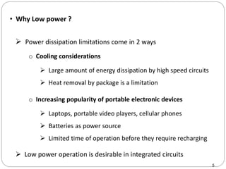
- 5. • Why Low power ? 5 Power dissipation limitations come in 2 ways Low power operation is desirable in integrated circuits o Cooling considerations Large amount of energy dissipation by high speed circuits Heat removal by package is a limitation o Increasing popularity of portable electronic devices Laptops, portable video players, cellular phones Batteries as power source Limited time of operation before they require recharging
- 6. 6 ADVANTAGES OF GDI OVER CMOS • Low power circuit design • Allows reducing power consumption • Reducing propagation delay • Reducing area of digital circuit • Maintaining low complexity of logic design
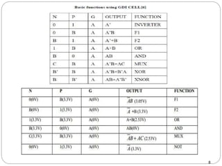
- 7. 7 BASIC GDI CELL FUNCTIONS • Reminds the standard CMOS inverter • Basic structure 3 inputs 1 output Bulk of both NMOS & PMOS are connected to N or P respectively o G (common gate input of NMOS & PMOS) o P (input to the source/drain of PMOS) o N (input to the source/drain of NMOS ) o D
- 8. 8
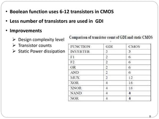
- 9. • Boolean function uses 6-12 transistors in CMOS • Less number of transistors are used in GDI • Improvements Design complexity level Transistor counts Static Power dissipation 9
- 10. TRANSIENT ANALYSIS OF BASIC GATE DIFFUSION INPUT (GDI) FUNCTIONS 10 • v(1) : Input voltage at G • v(2) : Input voltage at P • v(4) : Input voltage at N • v(3) : Output voltage at D
- 11. 11
- 12. 12
- 13. 13 OPERATIONAL ANALYSIS • Problem with pass transistor logic : low voltage swing • For function F1 • Low swing occurs in output when A=0 & B=0 • Expected Vtp = 0 v , due to poor high to low transition chara. of PMOS Vtp =.50v
- 14. 14 • Extra buffer circuitry may eliminate low voltage swing • About 50% of GDI cell operates as regular CMOS inverter • Used as a digital buffer for logic level restoration • In some cases, when VDD= 1 without a swing from the previous stages, a GDI functions as an inverter buffer and recovers the voltage swing
- 15. 15 COMPARISION WITH CMOS LOGIC STYLES • Circuits were designed in 0.35µm twin well CMOS technology • Simulated using AIMSPICE at 3.3V with load capacitance =100 fF
- 16. 16 • GDI have the lowest transistor count • Both power and delay are less in case of GDI technique
- 17. 17 CONVENTIONAL CMOS 1-BIT FULL ADDER • In VLSI application, arithmetic operations play important role • 1 bit full adder is building block of all operations • CMOS 1 bit full adder Addition Subtraction Multiplication Inputs : A, B, Cin (1 bit) Outputs : Sum, Carry (1 bit)
- 18. • CMOS design style is not area efficient for complex gates • CMOS full adder cell has 28 transistors • Pseudo NMOS • Dynamic logic • CMOS logic Static power consumption is high Compromise noise margin Charge leakage Charge sharing PMOS pull up & NMOS pull down network Number of transistors used is high o Requires frequent refreshing 18
- 19. 19
- 20. XOR BASED FULL ADDER • Equation obtained earlier can be modified as • Full adder can be implemented as 2 XOR gate and 1 mux using GDI cell 20
- 21. GDI CELL FOR XOR GATE • Only 4 transistors are used 21
- 22. GDI CELL FOR 1-BIT FULL ADDER • Built from two XOR gate and one MUX • Number of transistors used is reduced to 10 22
- 23. TRANSIENT ANALYSIS OF GDI BASED 1-BIT FULL ADDER • Inputs : v(1) –A, v(4)-B, v(7)-Cin • Outputs : v(8) – sum , v(9)- Cout 23
- 25. CONCLUSION • 2-Transistor implementation of complex logic functions • In-cell swing restoration under certain operating conditions • Low power design technique • New Circuit is most energy efficient cell compared to CMOS circuits • Issue of sequential logic design is currently being explored • Works are going on in automation of a logic design methodology on Gate Diffusion Input cells 25
- 26. REFERENCES • WEBSITES www.ijecse.org ieeexplore.ieee.org/ Implementation of 1-bit Full Adder using Gate Difuision Input (GDI) cell,Arun Prakash Singh 1, Rohit Kumar 2:1,Electronics and Communication Engineering Department, Northern India Engineering College,Lucknow, Uttar Pradesh, India.2.Electronics and Communication Engineering Department, Krishna Girls Engineering College A. Morgenshtein, A. Fish, I. A. Wagner,” Gate Diffusion Input (GDI) – A Novel Power Efficient Method for Digital Circuits: A Design Methodology”, 14th ASIC/SOC Conference, Washington D.C., USA, September 2001. and more.... • PAPERS REFERED 26
- 27. 27 THANK YOU 27