


![Arithmetic Instructions
MUL AB B:A = A * B 1
DIV AB A = [A/B] 1
DA A Decimal adjustment of 1
accumulator according to BCD
code](https://image.slidesharecdn.com/microcontrollerinstructionset-250407014238-9c070268/85/instruction_set_8051_microcontroller-ppt-41-320.jpg)


More Related Content
Similar to instruction_set_8051_microcontroller.ppt (20)
Recently uploaded (20)

![COMPUTER GRAPHICS AND VISUALIZATION :MODULE-1 notes [BCG402-CG&V].pdf](https://cdn.slidesharecdn.com/ss_thumbnails/module-1notesbcg402-cgv-250506151048-0a0d458b-thumbnail.jpg?width=560&fit=bounds)


![COMPUTER GRAPHICS AND VISUALIZATION :MODULE-02 notes [BCG402-CG&V].pdf](https://cdn.slidesharecdn.com/ss_thumbnails/module-02notesbcg402-cgv-250506151048-aef09ce3-thumbnail.jpg?width=560&fit=bounds)


instruction_set_8051_microcontroller.ppt
- 1. MICROCONTROLLER INSTRUCTION SET Subject: MICROCONTROLLER AND EMBEDED SYSTEM Class: 5th , ECE
- 2. Introduction An instruction is an order or command given to a processor by a computer program. All commands are known as instruction set and set of instructions is known as program. 8051 have in total 111 instructions, i.e. 111 different words available for program writing.
- 3. Instruction Format Where first part describes WHAT should be done, while other explains HOW to do it. The latter part can be a data (binary number) or the address at which the data is stored. Depending upon the number of bytes required to represent 1 instruction completely.
- 4. Types Of Instructions Instructions are divided into 3 types; 1. One/single byte instruction. 2. Two/double byte instruction. 3. Three/triple byte instruction.
- 5. Types Of Instructions 1. One/single byte instructions : If operand is not given in the instruction or there is no digits present with instruction, the instructions can be completely represented in one byte opcode. OPCODE 8 bit
- 6. Types Of Instructions 2. Two/double byte instruction: If 8 bit number is given as operand in the instruction, the such instructions can be completed represented in two bytes. First byte OPCODE Second byte 8 bit data or I/O port
- 7. Types Of Instructions 3. Three/triple byte instruction: If 16 bit number is given as operand in the instructions than such instructions can be completely represented in three bytes 16 bit number specified may be data or address.
- 8. Types Of Instructions 1. First byte will be instruction code. 2. Second byte will be 8 LSB’s of 16 bit number. 3. Third byte will be 8 MSB’s of 16 bit number. First byte OPCODE. Second byte 8 LSB’s of data/address. Third byte 8 MSB’S of data/address.
- 9. Addressing Modes Addressing modes specifies where the data (operand) is. They specify the source or destination of data (operand) in several different ways, depending upon the situation. Addressing modes are used to know where the operand located is.
- 10. Addressing Modes There are 5 types of addressing modes: 1. Register addressing. 2. Direct addressing. 3. Register indirect addressing. 4. Immediate addressing. 5. Index addressing.
- 11. Register Addressing Mode In register addressing mode; the source and/or destination is a register. In this case; data is placed in any of the 8 registers(R0-R7); in instructions it is specified with letter Rn (where N indicates 0 to 7).
- 12. Register Addressing Mode For example; 1. ADD A, Rn (This is general instruction). 2. ADD A, R5 (This instruction will add the contents of register R5 with the accumulator contents).
- 13. Direct Addressing Mode In direct addressing mode; the address of memory location containing data to be read is specified in instruction. In this case; address of the data is given with the instruction itself.
- 14. Direct Addressing Mode For example; 1. MOV A, 25H (This instruction will read/move the data from internal RAM address 25H and store it in the accumulator.
- 15. Register Indirect Addressing Mode In register indirect addressing mode; the contents of the designated register are used as a pointer to memory. In this case; data is placed in memory, but address of memory location is not given directly with instruction.
- 16. Register Indirect Addressing Mode For example; 1. MOV A,@R0 This instruction moves the data from the register whose address is in the R0 register into the accumulator.
- 17. Immediate Addressing Mode In immediate addressing mode, the data is given with the instruction itself. In this case; the data to be stored in memory immediately follows the opcode.
- 18. Immediate Addressing Mode For example; 1. MOV A, #25H (This instruction will move the data 25H to accumulator.
- 19. Index Addressing Mode Offset (from accumulator) is added to the base index register( DPTR OR Program Counter) to form the effective address of the memory location. In this case; this mode is made for reading tables in the program memory.
- 20. Index Addressing Mode For example; 1. MOVC A, @ A + DPTR ( This instruction moves the data from the memory to accumulator; whose address is computed by adding the contents of accumulator and DPTR)
- 21. Types Of Instructions 1. Data transfer instructions. 2. Arithmetic instructions. 3. Logical instructions. 4. Logical instructions with bits. 5. Branch instructions.
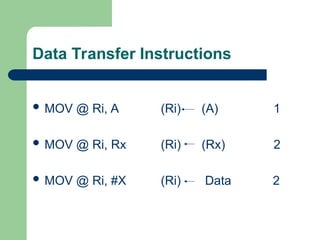
- 22. Data Transfer Instructions These instructions move the content of one register to another one. Data can be transferred to stack with the help of PUSH and POP instructions.
- 23. Data Transfer Instructions MNEMONIC DESCRIPTION BYTES MOV A,Rn (A) (Rn) 1 MOV A,Rx (A) (Rx) 2 MOV A,@Ri (A) (Ri) 1
- 24. Data Transfer Instructions MOV A,#X (A) Data 2 MOV Rn,A (Rn) (A) 1 MOV Rn, Rx (Rn) (Rx) 2
- 25. Data Transfer Instructions MOV Rn, #X (Rn) Data 2 MOV Rx, A (Rx) (A) 2 MOV Rx, Rn (Rx) (Rn) 2
- 26. Data Transfer Instructions MOV Rx, Ry (RX) (Ry) 3 MOV Rx, @ Ri (Rx) (Ri) 2 MOV Rx, # X (Rx) Data 3
- 27. Data Transfer Instructions MOV @ Ri, A (Ri) (A) 1 MOV @ Ri, Rx (Ri) (Rx) 2 MOV @ Ri, #X (Ri) Data 2
- 28. Data Transfer Instructions MOV DPTR, #X (DPTR) Data 3 MOVC A @ (A) (A+DPTR) 1 A+DPTR MOVC A@ (A) (A+PC) 1 A+PC
- 29. Data Transfer Instructions MOVX A,@ Ri A (Ri) 1 MOVX A, @ (A) (DPTR) 1 MOVX @Ri, A (Ri) (A) 1 DPTR
- 30. Data Transfer Instructions MOVX @ (DPTR) (A) 1 PUSH Rx Push directly 2 addressed Rx register on stack POP Rx (A) (Rx) 2 DPTR, A
- 31. Data Transfer Instructions XCH A, Rn (A) (Rn) 1 XCH A, Rx (A) (Rx) 2 XCH A, @Ri (A) (Ri) 1
- 32. Data Transfer Instructions XCHD Exchange 4 lower 1 bits in accumulator with indirectly addressed register
- 33. Arithmetic Instructions These instructions perform several basic operations. After execution, the result is stored in the first operand. 8 bit addition, subtraction, multiplication, increment-decrement instructions can be performed.
- 34. Arithmetic Instructions MNEMONICS DESCRIPTION BYTE ADD A, Rn A = A + Rn 1 ADD A, Rx A = A + Rx 2 AAD A, @ Ri A = A+ Ri 1
- 35. Arithmetic Instructions ADD A, # X A = A + Byte 2 ADDC A, Rn A = A + Rn + C 1 ADDC A , Rx A = A + Rx + C 2
- 36. Arithmetic Instructions ADDC A, @ Ri A = A + Ri + C 1 ADDC A, # X A = A + Byte + C 2 SUBB A, Rn A = A – Rn – 1 1
- 37. Arithmetic Instructions SUBB A, Rx A = A – Rx – 1 2 SUBB A, @ Ri A = A – Ri – 1 1 SUBB A, # X A = A – Byte – 1 2
- 38. Arithmetic Instructions INC A A = A + 1 1 INC Rn Rn = Rn + 1 1 INC Rx Rx = Rx + 1 2
- 39. Arithmetic Instructions INC @ Ri Ri = Ri + 1 1 DEC A A = A – 1 1 DEC Rn Rn = Rn – 1 1
- 40. Arithmetic Instructions DEC Rx Rx = Rx – 1 2 DEC @ Ri Ri = Ri – 1 1 INC DPTR DPTR = DPTR + 1 1
- 41. Arithmetic Instructions MUL AB B:A = A * B 1 DIV AB A = [A/B] 1 DA A Decimal adjustment of 1 accumulator according to BCD code
- 42. Logical Instructions These instructions perform logical operations between two register contents on bit by bit basis. After execution, the result is stored in the first operand.
- 43. Logical Instructions MNEMONIC DESCRIPTION BYTE ANL A, Rn (A) (A) ^ (Rn) 1 ANL A, Rx (A) (A) ^ (Rx) 2 ANL A,@ Ri (A) (A) ^ (Ri) 1
- 44. Logical Instructions ANL A, # X (A) (8 bit data) ^ (A) 2 ANL Rx, A (Rx) (A) ^ (Rx) 2 ANL Rx,# X (Rx) (8 bit data) ^ (Rx) 3
- 45. Logical Instructions ORL A, Rn (A) (A) + (Rn) 1 ORL A, Rx (A) (A) + (Rx) 2 ORL A, @ Ri (A) (A) + (Ri) 2
- 46. Logical Instructions ORL Rx, A (Rx) (A) + (Rx) 2 ORL Rx,# X (Rx) (8 bit data) + (Rx) 2 XORL A, Rn Logical exclusive 1 OR operation between the contents of accumulator and R register.
- 47. Logical Instructions XORL A, Rx Logical exclusive OR 2 operation between the contents of the accumulator and directly addressed register Rx. XORL A,@ Ri Logical exclusive OR 1 operation between the contents of the accumulator and directly addressed register.
- 48. Logical Instructions XORL A, # X Logical exclusive OR 2 operation between the contents of accumulator and the given 8 bit data. XORL Rx, A Logical exclusive OR 2 operation between the contents of the accumulator and directly addressed register Rx.
- 49. Logical Instructions XORL Rx, # X Logical exclusive OR 3 operation between the contents of the directly addressed register Rx and the given 8 bit data. CLR A (A) 0 1 CPL A (A) (/A) 1
- 50. Logical Instructions SWAP A (A3-0) (A7-4) 1 RL A (An + 1) (An) 1 (A0) (A7) RLC (An + 1) (An) 1 (A0) ( C ) ( C ) (A7)
- 51. Logical Instructions RR A (An) (An + 1) 1 (A7) (A0) RRC A (An) (An + 1) 1 (A7) ( C ) ( C ) (A0)
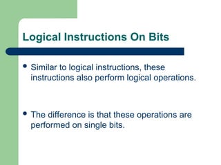
- 52. Logical Instructions On Bits Similar to logical instructions, these instructions also perform logical operations. The difference is that these operations are performed on single bits.
- 53. Logical Instructions On Bits MNEMONIC DESCRIPTION BYTE CLR C ( C = 0 ) 1 CLR bit clear directly addressed bit 2 SETB C ( C = 1 ) 1
- 54. Logical Instructions On Bits SETB bit Set directly 2 addressed bit CPL C (1 = 0, 0 = 1) 1 CPL bit Complement directly 2 addressed bit
- 55. Logical Instructions On Bits ANL C, bit Logical AND operation 2 between Carry bit and directly addressed bit. ANL C,/bit Logical AND operation 2 between Carry bit and inverted directly addressed bit.
- 56. Logical Instructions On Bits ORL C, bit Logical OR operation 2 between Carry bit and directly addressed bit. ORL C,/bit Logical OR operation 2 between Carry bit and inverted directly addressed bit.
- 57. Logical Instructions On Bits MOV C, bit Move directly addressed 2 bit to carry bit. MOV bit, C Move Carry bit to directly 2 addressed bit.
- 58. Program Flow Control Instructions In this group, instructions are related to the flow of the program, these are used to control the operation like, JUMP and CALL instructions. Some instructions are used to introduce delay in the program, to the halt program.
- 59. Program Flow Control Instructions MNEMONIC DESCRIPTION BYTE ACALL adr11 (PC) (PC) + 2 2 (SP) (SP) + 1 ((SP)) (PC7 – 0) (SP) (SP) + 1 ((SP)) (PC15-8)
- 60. Program Flow Control Instructions LCALL adr16 (PC) (PC) + 3 3 (SP) (SP) + 1 ((SP)) (PC7-0) (SP) (SP) + 1 ((SP)) (PC15-8) (PC) addr15-0
- 61. Program Flow Control Instructions RET (PC15-8) ((SP)) 1 (SP) (SP) – 1 (PC7-0) ((SP)) (SP) (SP) - 1
- 62. Program Flow Control Instructions RET1 (PC15-8) ((SP)) 1 (SP) (SP) – 1 (PC7-0) ((SP)) (SP) (SP) – 1 AJMP addr11 (PC) (PC) + 2 1 (PC10-0) page address
- 63. Program Flow Control Instructions LJMP addr16 (PC) addr15-0 3 SJMP rel short jump from 2 (from -128 to +127 locations in relation to first next instruction)
- 64. Program Flow Control Instructions JC rel (PC) (PC) + 2 2 IF ( C ) = 1 THEN (PC) (PC) + rel JNC rel (PC) (PC) + 2 2 IF ( C) = 0 THEN (PC) (PC) + rel
- 65. Program Flow Control Instructions JB bit, rel Jump if addressed 3 bit is set. Short jump. JBC bit, rel Jump if addressed 3 bit is set and clear it. Short jump.
- 66. Program Flow Control Instructions JMP @A + DPTR (PC) (A) + (DPTR) 1 JZ rel (PC) (PC) + 2 2 IF (A) = 0 THEN (PC) (PC) + rel
- 67. Program Flow Control Instructions JNZ rel (PC) (PC) + 2 2 IF (A) = 0 THEN (PC) (PC) + rel CJNE A, Rx, rel Compare the contents 3 of acc. And directly addressed register Rx. Jump if they are different. Short jump.
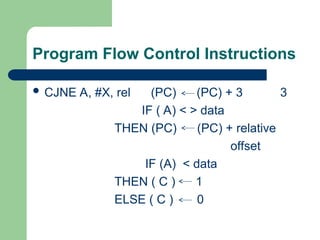
- 68. Program Flow Control Instructions CJNE A, #X, rel (PC) (PC) + 3 3 IF ( A) < > data THEN (PC) (PC) + relative offset IF (A) < data THEN ( C ) 1 ELSE ( C ) 0
- 69. Program Flow Control Instructions CJNE @ RI, # x, rel (PC) (PC) + 3 3 IF (Rn) <> data THEN (PC) (PC) + relative offset IF (Rn) < data THEN ( C ) 1 ELSE ( C ) 0
- 70. Program Flow Control Instructions CJNE @ Ri, # X, rel (PC) (PC) + 3 3 IF ((Ri)) <> data THEN (PC) (PC) + relative offset IF ((Ri)) < data THEN ( C ) 1 ELSE ( C ) 0
- 71. Program Flow Control Instructions DJNZ Rn , rel (PC) (PC) + 2 2 (Rn) (Rn) - 1 IF (Rn) > 0 or (Rn) < 0 THEN (PC) (PC) + rel
- 72. Program Flow Control Instructions DJNZ Rx, rel (PC) (PC) + 2 3 (Rx) (Rn) – 1 IF (Rx) > 0 or (Rx) < 0 THEN (PC) (PC) + rel NOP No operation 1
- 73. Summary Instruction set. Addressing modes. Data transfer instruction. Arithmetic instruction. Logical instruction. Logical operation on bits.