


![Special Function Registers [SFR]
8051 Microcontroller 26](https://image.slidesharecdn.com/unit1-240621044110-2cd739b1/85/INTRODUCTION-TO-MICROCONTROLLERS-8051-ARCHITECTURE-INSTRUCTION-SET-ADDRESSING-MODES-26-320.jpg)
![Internal RAM Structure
Direct &
Indirect
Addressing
Direct
Addressing
Only
SFR [ Special Function
Registers]
128 Byte Internal RAM
8051 Microcontroller 27](https://image.slidesharecdn.com/unit1-240621044110-2cd739b1/85/INTRODUCTION-TO-MICROCONTROLLERS-8051-ARCHITECTURE-INSTRUCTION-SET-ADDRESSING-MODES-27-320.jpg)
![Program Status Word [PSW]
8051 Microcontroller 28
C AC F0 RS1 RS0 OV -- P
Register Bank Select
Carry
Auxiliary Carry
User Flag 0
Parity
Reserved for future use
Overflow](https://image.slidesharecdn.com/unit1-240621044110-2cd739b1/85/INTRODUCTION-TO-MICROCONTROLLERS-8051-ARCHITECTURE-INSTRUCTION-SET-ADDRESSING-MODES-28-320.jpg)


![Arithmetic Instruction
• DEC A A = A – 1 1
• DEC Rn Rn = Rn – 1 1
• DEC @ Ri Ri = Ri – 1 1
• INC DPTR DPTR = DPTR + 1 1
• MUL AB B:A = A * B 1
• DIV AB A = [A/B] 1
• DA A Decimal adjustment of 1
accumulator according
to BCD code
8051 Microcontroller 63](https://image.slidesharecdn.com/unit1-240621044110-2cd739b1/85/INTRODUCTION-TO-MICROCONTROLLERS-8051-ARCHITECTURE-INSTRUCTION-SET-ADDRESSING-MODES-63-320.jpg)


INTRODUCTION TO MICROCONTROLLERS(8051) ARCHITECTURE,INSTRUCTION SET ,ADDRESSING MODES
- 2. The necessary tools for a microprocessor/controller 1. CPU: Central Processing Unit 2. I/O: Input /Output 3. Bus: Address bus & Data bus 4. Memory: RAM & ROM 5. Timer 6. Interrupt 7. Serial Port 8. Parallel Port 8051 Microcontroller 2
- 3. Internal Block Diagram of CPU 8051 Microcontroller 3
- 4. Address and Data Bus 8051 Microcontroller 4
- 5. Microcontroller • A smaller computer • On-chip RAM, ROM, I/O ports... • Example: Motorola’s 6811, Intel’s 8051, Zilog’s Z8 and PIC 8051 Microcontroller 5
- 6. Microprocessors • CPU for Computers • No RAM, ROM, I/O on CPU chip itself • Example: Intel's x86, Motorola’s 680x0 8051 Microcontroller 6
- 7. Microprocessor vs. Microcontroller Microprocessor • CPU is stand-alone, RAM, ROM, I/O, timer are separate • Designer can decide on the amount of ROM, RAM and I/O ports. • Expensive • Versatility • General-purpose Microcontroller • CPU, RAM, ROM, I/O and timer are all on a single chip • Fix amount of on-chip ROM, RAM, I/O ports • For applications in which cost, power and space are critical • Not Expensive • Single-purpose 8051 Microcontroller 7
- 8. Microcontrollers for Embedded Systems • Home – Appliances, intercom, telephones, security systems, garage door openers, answering machines, fax machines, home computers, TVs, cable TV tuner, VCR, camcorder, remote controls, video games, cellular phones, musical instruments, sewing machines, lighting control, paging, camera, pinball machines, toys, exercise equipment etc. • Office – Telephones, computers, security systems, fax machines, microwave, copier, laser printer, color printer, paging etc. • Auto – Trip computer, engine control, air bag, ABS, instrumentation, security system, transmission control, entertainment, climate control, cellular phone, keyless entry 8051 Microcontroller 8
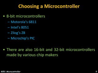
- 9. Choosing a Microcontroller • 8-bit microcontrollers – Motorola’s 6811 – Intel’s 8051 – Zilog’s Z8 – Microchip’s PIC • There are also 16-bit and 32-bit microcontrollers made by various chip makers 8051 Microcontroller 9
- 10. Criteria for Choosing a Microcontroller • Meeting the computing needs of the task at hand efficiently and cost effectively – Speed – Packaging – Power consumption – The amount of RAM and ROM on chip – The number of I/O pins and the timer on chip – How easy to upgrade to higher performance or lower power- consumption versions – Cost per unit 8051 Microcontroller 10
- 11. Criteria for Choosing a Microcontroller • Availability of software development tools, such as compilers, assemblers, and debuggers • Wide availability and reliable sources of the microcontroller – The 8051 family has the largest number of diversified (multiple source) suppliers • Intel (original) • Atmel • Philips/Signetics • AMD • Infineon (formerly Siemens) • Matra • Dallas Semiconductor/Maxim 8051 Microcontroller 11
- 12. 8051 Microcontroller • Intel introduced 8051, referred as MCS- 51, in 1981. • The 8051 is an 8-bit processor – The CPU can work on only 8 bits of data at a time • The 8051 became widely popular after allowing other manufactures to make and market any flavor of the 8051. 8051 Microcontroller 12
- 13. 8051 Family • The 8051 is a subset of the 8052 • The 8031 is a ROM-less 8051 – Add external ROM to it – You lose two ports, and leave only 2 ports for I/O operations 8051 Microcontroller 13
- 14. 8051 Features • 64KB Program Memory address space • 64KB Data Memory address space • 4K bytes of on-chip Program Memory • 128 bytes of on-chip Data RAM • 32 bidirectional and individually addressable I/0 lines • Two 16-bit timer/counters • Full duplex UART • 6-source/5-vector interrupt structure with two priority levels • On-chip clock oscillator 8051 Microcontroller 14
- 15. Pin Diagram of the 8051 8051 Microcontroller 15
- 16. Interrupt Control CPU 4K ROM 128 B RAM OSC Bus Control 4 I/O Ports Serial Port Timer 1 Timer 0 General Block Diagram of 8051 TXD RXD P0 P1 P2 P3 8051 Microcontroller 16
- 17. Detailed Block Diagram 8051 Microcontroller 17
- 19. 8051 Memory Structure External INT 128 SFR External Program Memory Data Memory 64K EA = 0 EA = 1 4K 64K 8051 Microcontroller 19
- 20. 128 Byte RAM • There are 128 bytes of RAM in the 8051. – Assigned addresses 00 to 7FH • The 128 bytes are divided into 3 different groups as follows: 1. A total of 32 bytes from locations 00 to 1F hex are set aside for register banks and the stack. 2. A total of 16 bytes from locations 20H to 2FH are set aside for bit-addressable read/write memory. 3. A total of 80 bytes from locations 30H to 7FH are used for read and write storage, called scratch pad. 8051 Microcontroller 20 128 BYTE INTERNAL RAM Register Banks Reg Bank 0 Reg Bank 1 Reg Bank 2 Reg Bank 3 BIT Addressable Area General Purpose Area
- 21. 8051 Programming Model 8051 Microcontroller 21
- 22. 8051 RAM with addresses 8051 Microcontroller 22
- 23. 8051 Register Banks with address 8051 Microcontroller 23
- 24. Bit Addressable & Byte Addressable 8051 Microcontroller 24
- 25. Bit Addressable Programming • Example: Find out to which by each of the following bits belongs. Give the address of the RAM byte in hex (a) SETB 42H, (b) CLR 67H, (c) CLR 0FH (d) SETB 28H, (e) CLR 12, (f) SETB 05 8051 Microcontroller 25
- 26. Special Function Registers [SFR] 8051 Microcontroller 26
- 27. Internal RAM Structure Direct & Indirect Addressing Direct Addressing Only SFR [ Special Function Registers] 128 Byte Internal RAM 8051 Microcontroller 27
- 28. Program Status Word [PSW] 8051 Microcontroller 28 C AC F0 RS1 RS0 OV -- P Register Bank Select Carry Auxiliary Carry User Flag 0 Parity Reserved for future use Overflow
- 29. Flags in PSW 8051 Microcontroller 29
- 30. Flags in PSW 8051 Microcontroller 30
- 31. Flags in PSW 8051 Microcontroller 31
- 32. Example for Overflow flag 8051 Microcontroller 32
- 33. 8051 instructions that affects flag 8051 Microcontroller 33
- 34. 8051 Stack • The stack is a section of RAM used by the CPU to store information temporarily. – This information could be data or an address • The register used to access the stack is called the SP (stack pointer) register – The stack pointer in the 8051 is only 8 bit wide, which means that it can take value of 00 to FFH – When the 8051 is powered up, the SP register contains value 07 – RAM location 08 is the first location begin used for the stack by the 8051 8051 Microcontroller 34
- 35. 8051 Stack • The storing of a CPU register in the stack is called a PUSH – SP is pointing to the last used location of the stack – As we push data onto the stack, the SP is incremented by one – This is different from many microprocessors • Loading the contents of the stack back into a CPU register is called a POP – With every pop, the top byte of the stack is copied to the register specified by the instruction and the stack pointer is decremented once 8051 Microcontroller 35
- 36. Pushing onto Stack 8051 Microcontroller 36
- 37. Popping from Stack 8051 Microcontroller 37
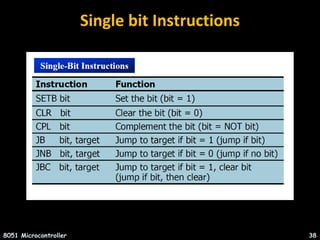
- 38. Single bit Instructions 8051 Microcontroller 38
- 39. 8051 Addressing Modes • The CPU can access data in various ways, which are called addressing modes 1. Immediate 2. Register 3. Direct 4. Register indirect 5. External Direct 8051 Microcontroller 39
- 40. Immediate Addressing Mode • The source operand is a constant. • The immediate data must be preceded by the pound sign, “#” • Can load information into any registers, including 16-bit DPTR register – DPTR can also be accessed as two 8-bit registers, the high byte DPH and low byte DPL 8051 Microcontroller 40
- 41. Register Addressing Mode • Use registers to hold the data to be manipulated. 8051 Microcontroller 41 • The source and destination registers must match in size. MOV DPTR,A will give an error • The movement of data between Rn registers is not allowed MOV R4,R7 is invalid
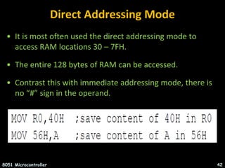
- 42. Direct Addressing Mode • It is most often used the direct addressing mode to access RAM locations 30 – 7FH. • The entire 128 bytes of RAM can be accessed. • Contrast this with immediate addressing mode, there is no “#” sign in the operand. 8051 Microcontroller 42
- 43. SFR Registers & their Addresses MOV 0E0H,#55H ;is the same as MOV A,#55H ;which means load 55H into A (A=55H) MOV 0F0H,#25H ;is the same as MOV B,#25H ;which means load 25H into B (B=25H) MOV 0E0H,R2 ;is the same as MOV A,R2 ;which means copy R2 into A MOV 0F0H,R0 ;is the same as MOV B,R0 ;which means copy R0 into B 8051 Microcontroller 43
- 44. SFR Addresses ( 1 of 2 ) 8051 Microcontroller 44
- 45. SFR Addresses ( 2 of 2 ) 8051 Microcontroller 45
- 47. Stack and Direct Addressing Mode • Only direct addressing mode is allowed for pushing or popping the stack. • PUSH A is invalid. • Pushing the accumulator onto the stack must be coded as PUSH 0E0H. 8051 Microcontroller 47
- 48. Register Indirect Addressing Mode • A register is used as a pointer to the data. • Only register R0 and R1 are used for this purpose. • R2 – R7 cannot be used to hold the address of an operand located in RAM. • When R0 and R1 hold the addresses of RAM locations, they must be preceded by the “@” sign. 8051 Microcontroller 48
- 49. Register Indirect Addressing Mode • The advantage is that it makes accessing data dynamic rather than static as in direct addressing mode. • Looping is not possible in direct addressing mode. • Write a program to clear 16 RAM locations starting at RAM address 60H. 8051 Microcontroller 49
- 50. Index Addressing Mode For example 1. MOVC A, @ A + DPTR ( This instruction moves the data from the memory to accumulator; whose address is computed by adding the contents of accumulator and DPTR) NMAMIT 8051 Microcontroller 50
- 51. External Direct • External Memory is accessed. • There are only two commands that use External Direct addressing mode: – MOVX A, @DPTR MOVX @DPTR, A • DPTR must first be loaded with the address of external memory. 8051 Microcontroller 51
- 52. Register Indirect Addressing Mode • Write a program to copy the value 55H into RAM memory locations 40H to 41H using (a) direct addressing mode, (b) register indirect addressing mode without a loop, and (c) with a loop. 8051 Microcontroller 52
- 53. 8051 Instruction Set • DATA TRANSFER GROUP • ARITHMETIC GROUP • LOGICAL GROUP • CONTROL TRANSFER GROUP 8051 Microcontroller 53
- 54. Structure of Assembly Language ORG 0H ;start (origin) at location 0 MOV R5,#25H ;load 25H into R5 MOV R7,#34H ;load 34H into R7 MOV A,#0 ;load 0 into A ADD A,R5 ;add contents of R5 to A ;now A = A + R5 ADD A,R7 ;add contents of R7 to A ;now A = A + R7 ADD A,#12H ;add to A value 12H ;now A = A + 12H HERE: SJMP HERE ;stay in this loop END ;end of asm source file 8051 Microcontroller 54
- 55. Data Types & Directives ORG 500H DATA1: DB 28 ;DECIMAL (1C in Hex) DATA2: DB 00110101B ;BINARY (35 in Hex) DATA3: DB 39H ;HEX ORG 510H DATA4: DB “2591” ; ASCII NUMBERS ORG 518H DATA6: DB “My name is Joe” ;ASCII CHARACTERS 8051 Microcontroller 55
- 56. Data Transfer Instructions MNEMONIC DESCRIPTION BYTES • MOV A, Rn (A) (Rn) 1 • MOV A, Rx (A) (Rx) 2 • MOV A,@Ri (A) (Ri) 1 • MOV A, #X (A) Data 2 • MOV Rn, A (Rn) (A) 1 • MOV Rn,#X (Rn) Data 2 • MOV Rx,A (Rx) (A) 2 8051 Microcontroller 56
- 57. Data Transfer Instructions MNEMONIC DESCRIPTION BYTES • MOV Rx, @ Ri (Rx) (Ri) 2 • MOV Rx, # X (Rx) Data 3 • MOV @ Ri, A (Ri) (A) 1 • MOV @ Ri, Rx (Ri) (Rx) 2 • MOV @ Ri, #X (Ri) Data 2 • MOV DPTR, #X (DPTR) Data 3 • MOVC A @ A+DPTR (A) (A+DPTR) 1 • MOVC A@A+PC (A) (A+PC) 1 8051 Microcontroller 57
- 58. Data Transfer Instructions MNEMONIC DESCRIPTION BYTES • MOVX A, @ DPTR (A) (DPTR) 1 • MOVX @Ri, A (Ri) (A) 1 • MOVX A,@ Ri A (Ri) 1 • XCH A, Rn (A) (Rn) 1 • XCH A, Rx (A) (Rx) 2 • XCH A, @Ri (A) (Ri) 1 • MOVX @DPTR, A (DPTR) (A) 1 • PUSH Rx Push directly addressed 2 Rx register on stack • POP Rx (A) (Rx) 2 8051 Microcontroller 58
- 59. Data Transfer Instructions • XCHD Exchange 4 lower bits in 1 accumulator with indirectly addressed register 8051 Microcontroller 59
- 60. MOV Instruction • MOV destination, source ; copy source to destination. • MOV A,#55H ;load value 55H into reg. A MOV R0,A ;copy contents of A into R0 ;(now A=R0=55H) MOV R1,A ;copy contents of A into R1 ;(now A=R0=R1=55H) MOV R2,A ;copy contents of A into R2 ;(now A=R0=R1=R2=55H) MOV R3,#95H ;load value 95H into R3 ;(now R3=95H) MOV A,R3 ;copy contents of R3 into A ;now A=R3=95H 8051 Microcontroller 60
- 61. Arithmetic Instructions • These instructions perform several basic operations. After execution, the result is stored in the first operand. • 8 bit addition, subtraction, multiplication, increment- decrement instructions can be performed. MNEMONICS DESCRIPTION BYTE • ADD A, Rn A = A + Rn 1 • ADD A, @ Ri A = A+ Ri 1 • ADD A, # X A = A + Byte 2 • ADDC A, Rn A = A + Rn + C 1 8051 Microcontroller 61
- 62. Arithmetic Instruction • ADDC A, @ Ri A = A + Ri + C 1 • ADDC A, # X A = A + Byte + C 2 • SUBB A, Rn A = A – Rn – 1 1 • SUBB A, @ Ri A = A – Ri – 1 1 • SUBB A, # X A = A – Byte – 1 2 • INC A A = A + 1 1 • INC Rn Rn = Rn + 1 1 • INC @ Ri Ri = Ri + 1 1 8051 Microcontroller 62
- 63. Arithmetic Instruction • DEC A A = A – 1 1 • DEC Rn Rn = Rn – 1 1 • DEC @ Ri Ri = Ri – 1 1 • INC DPTR DPTR = DPTR + 1 1 • MUL AB B:A = A * B 1 • DIV AB A = [A/B] 1 • DA A Decimal adjustment of 1 accumulator according to BCD code 8051 Microcontroller 63
- 64. ADD Instruction • ADD A, source ;ADD the source operand to the accumulator • MOV A, #25H ;load 25H into A MOV R2,#34H ;load 34H into R2 ADD A,R2 ;add R2 to accumulator ;(A = A + R2) 8051 Microcontroller 64
- 69. DECIMAL ADJUST for Addition 8051 Microcontroller 69
- 70. ASCII TO BCD and BCD TO ASCII 8051 Microcontroller 70
- 71. Multiplication of Unsigned Numbers MUL AB ; A B, place 16-bit result in B and A MOV A,#25H ;load 25H to reg. A MOV B,#65H ;load 65H in reg. B MUL AB ;25H * 65H = E99 where B = 0EH and A = 99H Table 6-1:Unsigned Multiplication Summary (MUL AB) Multiplication Operand 1 Operand 2 Result byte byte A B A=low byte, B=high byte 8051 Microcontroller 71
- 73. Division of Unsigned Numbers DIV AB ; divide A by B • MOV A,#95H ;load 95 into A • MOV B,#10H ;load 10 into B • DIV AB ;now A = 09 (quotient) and B = 05 (remainder) 8051 Microcontroller 73 Table 6-2:Unsigned Division Summary (DIV AB) Division Numerator Denominator Quotient Remainder byte / byte A B A B
- 84. Program Flow Control Instructions 8051 Microcontroller 84
- 85. Program Flow Control Instructions 8051 Microcontroller 85
- 86. PROGRAM USING LCALL INSTRUCTION 8051 Microcontroller 86
- 87. Program Flow Control Instructions 8051 Microcontroller 87
- 88. Program Flow Control Instructions 8051 Microcontroller 88
- 89. Conditional Jump Example 8051 Microcontroller 89
- 90. Unconditional Jump Instructions • All conditional jumps are short jumps – Target address within -128 to +127 of PC • LJMP (long jump): 3-byte instruction – 2-byte target address: 0000 to FFFFH – Original 8051 has only 4KB on-chip ROM • SJMP (short jump): 2-byte instruction – 1-byte relative address: -128 to +127
- 91. Call Instructions • LCALL (long call): 3-byte instruction – 2-byte address – Target address within 64K-byte range • ACALL (absolute call): 2-byte instruction – 11-bit address – Target address within 2K-byte range
- 92. 8051 Software Overview 1. Addressing Modes 2.Instruction Set 3.Programming 8051 Microcontroller 92
- 93. Checking an input bit 8051 Microcontroller 93 JNB (jump if no bit) ; JB (jump if bit = 1)
- 94. Switch Register Banks 8051 Microcontroller 94
- 95. Pushing onto Stack 8051 Microcontroller 95
- 96. Popping from Stack 8051 Microcontroller 96
- 98. Loop inside a Loop (Nested Loop) 8051 Microcontroller 98
- 99. 8051 Conditional Jump Instructions 8051 Microcontroller 99
- 100. Conditional Jump Example 8051 Microcontroller 100
- 101. Unconditional Jump Instructions • All conditional jumps are short jumps – Target address within -128 to +127 of PC • LJMP (long jump): 3-byte instruction – 2-byte target address: 0000 to FFFFH – Original 8051 has only 4KB on-chip ROM • SJMP (short jump): 2-byte instruction – 1-byte relative address: -128 to +127 8051 Microcontroller 101
- 102. Conditional Jump Example 8051 Microcontroller 102
- 103. Call Instructions • LCALL (long call): 3-byte instruction – 2-byte address – Target address within 64K-byte range • ACALL (absolute call): 2-byte instruction – 11-bit address – Target address within 2K-byte range 8051 Microcontroller 103