


IO organization.ppt
- 1. INPUT/OUTPUT ORGANIZATION Presented By: S.DEEPA AP(Sr.G)/ CT-PG Kongu Engineering College
- 2. Outline Accessing I/O Devices Interrupts Handling Multiple Devices Exceptions Direct Memory Access Buses Interface Circuits Standard I/O Interfaces 2
- 3. Accessing I/O devices Bus I/O device 1 I/O device n Processor Memory • Multiple I/O devices may be connected to the processor and the memory via a bus. • Bus consists of three sets of lines to carry address, data and control signals. • Each I/O device is assigned an unique address. • To access an I/O device, the processor places the address on the address lines. • The device recognizes the address, and responds to the control signals. 3
- 4. Accessing I/O devices 4 I/O devices and the memory may share the same address space : Memory-mapped I/O Any machine instruction that can access memory can be used to transfer data to or from an I/O device. I/O devices and the memory may have different address spaces: Special instructions to transfer data to and from I/O devices. I/O devices may have to deal with fewer address lines. I/O address lines need not be physically separate from memory address lines. In fact, address lines may be shared between I/O devices and memory, with a control signal to indicate whether it is a memory address or an I/O address.
- 5. Accessing I/O devices I/O interface decoder Address Data and status registers Control circuits Input device Bus Address lines Data lines Control lines • I/O device is connected to the bus using an I/O interface circuit which has: - Address decoder, control circuit, and data and status registers. • Address decoder decodes the address placed on the address lines thus enabling the device to recognize its address. • Data register holds the data being transferred to or from the processor. • Status register holds information necessary for the operation of the I/O device. • Data and status registers are connected to the data lines, and have unique addresses. • I/O interface circuit coordinates I/O transfers. 5
- 6. Accessing I/O devices Recall that the rate of transfer to and from I/O devices is slower than the speed of the processor. This creates the need for mechanisms to synchronize data transfers between them. Program-controlled I/O: Processor repeatedly monitors a status flag to achieve the necessary synchronization. Processor polls the I/O device. Two other mechanisms used for synchronizing data transfers between the processor and memory: Interrupts. Direct Memory Access. 6
- 8. Accessing I/O devices-Example 8 A program that reads one line from keyboard, stores it in memory buffer, and prints it back to the display
- 9. Interrupts In program-controlled I/O, when the processor continuously monitors the status of the device, it does not perform any useful tasks. An alternate approach would be for the I/O device to alert the processor when it becomes ready. Do so by sending a hardware signal called an interrupt to the processor. At least one of the bus control lines, called an interrupt-request line is dedicated for this purpose. Processor can perform other useful tasks while it is waiting for the device to be ready. The routine executed in response to an interrupt request is called Interrupt Service Routine 9
- 10. Interrupts PRINT routine COMPUTE routine here Interrupt occurs M i 2 1 i 1 + • Processor is executing the instruction located at address i when an interrupt occurs. • Routine executed in response to an interrupt request is called the interrupt-service routine. • When an interrupt occurs, control must be transferred to the interrupt service routine. • But before transferring control, the current contents of the PC (i+1), must be saved in a known location. • This will enable the return-from-interrupt instruction to resume execution at i+1. • Return address, or the contents of the PC are usually stored on the processor stack. 10 Program 1 Interrupt Service routine
- 11. Interrupts Treating an interrupt-service routine is very similar to that of a subroutine. However there are significant differences: A subroutine performs a task that is required by the calling program. Interrupt-service routine may not have anything in common with the program it interrupts. Interrupt-service routine and the program that it interrupts may belong to different users. As a result, before branching to the interrupt-service routine, not only the PC, but other information such as condition code flags, and processor registers used by both the interrupted program and the interrupt service routine must be stored. This will enable the interrupted program to resume execution upon return from interrupt service routine. 11
- 12. Interrupts Saving and restoring information can be done automatically by the processor or explicitly by program instructions. Saving and restoring registers involves memory transfers: Increases the total execution time. Increases the delay between the time an interrupt request is received, and the start of execution of the interrupt-service routine. This delay is called interrupt latency. In order to reduce the interrupt latency, most processors save only the minimal amount of information: This minimal amount of information includes Program Counter and processor status registers. Any additional information that must be saved, must be saved explicitly by the program instructions at the beginning of the interrupt service routine. 12
- 13. Interrupts When a processor receives an interrupt-request, it must branch to the interrupt service routine. It must also inform the device that it has recognized the interrupt request. This can be accomplished in two ways: Some processors have an explicit interrupt-acknowledge control signal for this purpose. In other cases, the data transfer that takes place between the device and the processor can be used to inform the device. 13
- 14. Interrupt Hardware A single interrupt line may be used to serve n devices. All devices are connected to the line via switches to ground. To re quest an interrupt, a device closes its associated switch. If all switches are open, the voltage on the interrupt-request line will be equal to Vdd. This is the inactive state of the line. Since closing of one or more switches will cause the line voltage to drop to 0, the value of INTR is the logical OR of the requests from individual device. INTR = INTR1+….+INTRn 14
- 15. Enabling & Disabling Interrupts Interrupt-requests interrupt the execution of a program, and may alter the intended sequence of events: Sometimes such alterations may be undesirable, and must not be allowed. For example, the processor may not want to be interrupted by the same device while executing its interrupt-service routine. Processors generally provide the ability to enable and disable such interruptions as desired. One simple way is to provide machine instructions such as Interrupt-enable and Interrupt-disable for this purpose. 3 mechanisms to enable and disable interrupts At the device end: To avoid interruption by the different device during the execution of an interrupt service routine: First instruction of an interrupt service routine can be Interrupt-disable. Last instruction of an interrupt service routine can be Interrupt-enable. 15
- 16. Enabling & Disabling Interrupts At the processor end: The processor automatically disable interrupts before starting the execution of the interrupt- service routine. After saving value of PC and processor status register on the stack, the processor executes interrupt-disable instruction by clearing the interrupt-enable bit to 0. When a return-from-interrupt instruction is executed, the contents of PS are restored from stack, setting the interrupt-enable bit to 1. Edge Triggered Interrupts: Interrupt handling circuit responds only to the leading edge of the signal. Processor receives only one request regardless of how long the line is activated. No need to explicitly disable interrupt requests. 16
- 17. Enabling & Disabling Interrupts Assuming that interrupts are enabled, the following is a typical scenario. The device raises an interrupt request The processor interrupts the program currently being executed Interrupts are disabled The device is informed that its request has been recognized The action requested by the interrupt is performed by the ISR Interrupts are enabled and execution of the interrupted program is resumed 17
- 18. Handling Multiple Devices Multiple I/O devices may be connected to the processor and the memory via a bus. Some or all of these devices may be capable of generating interrupt requests. Most common questions How does the processor know which device has generated an interrupt? How does the processor know which interrupt service routine needs to be executed? When the processor is executing an interrupt service routine for one device, can other device interrupt the processor? If two interrupt-requests are received simultaneously, then how to break the tie? 18
- 19. Handling Multiple Devices Consider a simple arrangement where all devices send their interrupt-requests over a single control line in the bus. When the processor receives an interrupt request over this control line, how does it know which device is requesting an interrupt? This information is available in the status register of the device requesting an interrupt: The status register of each device has an IRQ bit which it sets to 1 when it requests an interrupt. Interrupt service routine can poll the I/O devices connected to the bus. The first device with IRQ equal to 1 is the one that is serviced. Polling mechanism is easy, but time consuming to query the status bits of all the I/O devices connected to the bus. An alternative approach is to use vectored interrupts. 19
- 20. Vectored Interrupts The device requesting an interrupt may identify itself directly to the processor. Device can do so by sending a special code (4 to 8 bits) the processor over the bus. Code supplied by the device may represent a part of the starting address of the interrupt-service routine. The remainder of the starting address is obtained by the processor based on other information such as the range of memory addresses where interrupt service routines are located. Usually the location pointed to by the interrupting device is used to store the starting address of the interrupt-service routine. Processor reads this address (interrupt vector) and loads it into the PC 20
- 21. Interrupt Nesting Previously, before the processor started executing the interrupt service routine for a device, it disabled the interrupts from the device. In general, same arrangement is used when multiple devices can send interrupt requests to the processor. During the execution of an interrupt service routine of device, the processor does not accept interrupt requests from any other device. Since the interrupt service routines are usually short, the delay that this causes is generally acceptable. However, for certain devices this delay may not be acceptable. Which devices can be allowed to interrupt a processor when it is executing an interrupt service routine of another device? 21
- 22. Interrupt Nesting I/O devices are organized in a priority structure: An interrupt request from a high-priority device is accepted while the processor is executing the interrupt service routine of a low priority device. A priority level is assigned to a processor that can be changed under program control. Priority level of a processor is the priority of the program that is currently being executed. When the processor starts executing the interrupt service routine of a device, its priority is raised to that of the device. If the device sending an interrupt request has a higher priority than the processor, the processor accepts the interrupt request. 22
- 23. Interrupt Nesting Processor’s priority is encoded in a few bits of the processor status register. Priority can be changed by instructions that write into the processor status register. Usually, these are privileged instructions, or instructions that can be executed only in the supervisor mode. Privileged instructions cannot be executed in the user mode. Prevents a user program from accidentally or intentionally changing the priority of the processor. If there is an attempt to execute a privileged instruction in the user mode, it causes a special type of interrupt called as privilege exception. 23
- 24. Interrupt Nesting Priority arbitration Device 1 Device 2 Devicep Processor INTA1 INTR1 I NTRp INTA p • Each device has a separate interrupt-request and interrupt-acknowledge line. • Each interrupt-request line is assigned a different priority level. • Interrupt requests received over these lines are sent to a priority arbitration circuit in the processor. • If the interrupt request has a higher priority level than the priority of the processor, then the request is accepted. 24
- 25. Interrupts – Simultaneous Requests If processor receives interrupt requests from two or more devices simultaneously ,Which interrupt request does the processor accept?. If the I/O devices are organized in a priority structure, the processor accepts the interrupt request from a device with higher priority. Each device has its own interrupt request and interrupt acknowledge line. A different priority level is assigned to the interrupt request line of each device. 25
- 26. Interrupts – Simultaneous Requests Processor Device 2 I NTR INTA Device n Device 1 Polling scheme: • Processor uses a polling mechanism to poll the status registers of I/O devices to determine which device is requesting an interrupt. • In this case the priority is determined by the order in which the devices are polled. • The first device with status bit set to 1 is the device whose interrupt request is accepted. Daisy chain scheme: • Devices are connected to form a daisy chain. • Devices share the interrupt-request line, and interrupt-acknowledge line is connected to form a daisy chain. • When devices raise an interrupt request, the interrupt-request line is activated. • The processor in response activates interrupt-acknowledge. • Received by device 1, if device 1 does not need service, it passes the signal to device 2. • Device that is electrically closest to the processor has the highest priority. 26
- 27. Interrupts – Simultaneous Requests • When I/O devices were organized into a priority structure, each device had its own interrupt-request and interrupt-acknowledge line. • When I/O devices were organized in a daisy chain fashion, the devices shared an interrupt-request line, and the interrupt-acknowledge propagated through the devices. • A combination of priority structure and daisy chain scheme can also used. Device Device circuit Priority arbitration Processor Device Device I NTR1 INTRp INTA1 INTAp • Devices are organized into groups. • Each group is assigned a different priority level. • All the devices within a single group share an interrupt-request line, and are connected to form a daisy chain. 27
- 28. Controlling Device Requests Only those devices that are being used in a program should be allowed to generate interrupt requests. To control which devices are allowed to generate interrupt requests, the interface circuit of each I/O device has an interrupt-enable bit. If the interrupt-enable bit in the device interface is set to 1, then the device is allowed to generate an interrupt-request. Interrupt-enable bit in the device’s interface circuit determines whether the device is allowed to generate an interrupt request. Interrupt-enable bit in the processor status register or the priority structure of the interrupts determines whether a given interrupt will be accepted. 28
- 29. Controlling Device Requests Example: Program using interrupts to read a line of characters from a keyboard via the registers 29
- 30. Exceptions Interrupts caused by interrupt-requests sent by I/O devices. Interrupts could be used in many other situations where the execution of one program needs to be suspended and execution of another program needs to be started. In general, the term exception is used to refer to any event that causes an interruption. Interrupt-requests from I/O devices is one type of an exception. Other types of exceptions are: Recovery from errors Debugging Privilege Exception 30
- 31. Exceptions Recovery from errors Many sources of errors in a processor. For example: Error in the data stored. Error during the execution of an instruction. When such errors are detected, exception processing is initiated. Processor takes the same steps as in the case of I/O interrupt-request. It suspends the execution of the current program, and starts executing an exception-service routine. Difference between handling I/O interrupt-request and handling exceptions due to errors: In case of I/O interrupt-request, the processor usually completes the execution of an instruction in progress before branching to the interrupt- service routine. In case of exception processing however, the execution of an instruction in progress usually cannot be completed. 31
- 32. Exceptions Debugging Debugger uses exceptions to provide important features: Trace, Breakpoints. Trace mode: Exception occurs after the execution of every instruction. Debugging program is used as the exception-service routine. Enables the user to examine the contents of registers, memory location and so on. On return to from debugging program, the next instruction in the program being debugged is executed, then the debugging program is activated again. Breakpoints: Exception occurs only at specific points selected by the user. An instruction called trap or software-interrupt is usually provided for this purpose. Debugging program is used as the exception-service routine. 32
- 33. Exceptions Privilege Exception To protect the OS from being corrupted by user program, certain instructions can be executed only when the processor is in the supervisor mode. These are called privileged instructions. If an attempt is made to execute a privileged instruction in the user mode, a privilege exception occurs. Privilege exception causes: Processor to switch to the supervisor mode, Execution of an appropriate exception-servicing routine. 33
- 34. Direct Memory Access A special control unit may be provided to transfer a block of data directly between an I/O device and the main memory, without continuous intervention by the processor. Control unit which performs these transfers is a part of the I/O device’s interface circuit. This control unit is called as a DMA controller. DMA controller performs functions that would be normally carried out by the processor: For each word, it provides the memory address and all the control signals. To transfer a block of data, it increments the memory addresses and keeps track of the number of transfers. 34
- 35. Direct Memory Access DMA controller can transfer a block of data from an external device to the processor, without any intervention from the processor. However, the operation of the DMA controller must be under the control of a program executed by the processor. That is, the processor must initiate the DMA transfer. To initiate the DMA transfer, the processor informs the DMA controller of: Starting address, Number of words in the block. Direction of transfer (I/O device to the memory, or memory to the I/O device). Once the DMA controller completes the DMA transfer, it informs the processor by raising an interrupt signal. 35
- 37. Direct Memory Access memory Processor System bus Main Keyboard Disk/DMA controller Printer DMA controller Disk Disk • DMA controller connects a high-speed network to the computer bus. • Disk controller, which controls two disks also has DMA capability. It provides two DMA channels. • It can perform two independent DMA operations, as if each disk has its own DMA controller. The registers to store the memory address, word count and status and control information are duplicated. Network Interface 37
- 38. Direct Memory Access Processor and DMA controllers have to use the bus in an interwoven fashion to access the memory. DMA devices are given higher priority than the processor to access the bus. Among different DMA devices, high priority is given to high-speed peripherals such as a disk or a graphics display device. Processor originates most memory access cycles on the bus. DMA controller can be said to “steal” memory access cycles from the bus. This interweaving technique is called as “cycle stealing”. An alternate approach is the provide a DMA controller an exclusive capability to initiate transfers on the bus, and hence exclusive access to the main memory. This is known as the block or burst mode. 38
- 39. Bus Arbitration Processor and DMA controllers both need to initiate data transfers on the bus and access main memory. The device that is allowed to initiate transfers on the bus at any given time is called the bus master. When the current bus master relinquishes its status as the bus master, another device can acquire this status. The process by which the next device to become the bus master is selected and bus mastership is transferred to it is called bus arbitration. Centralized arbitration: A single bus arbiter performs the arbitration. Distributed arbitration: All devices participate in the selection of the next bus master. 39
- 40. Centralized Bus Arbitration Processor DMA controller 1 DMA controller 2 BG1 BG2 B R B BSY 40
- 42. Centralized Bus Arbitration Sequence of signals during transfer of bus mastership for devices BBSY BG1 BG2 Bus master BR Processor DMA controller 2 Processor Time DMA controller 2 asserts the BR signal. Processor asserts the BG1 signal BG1 signal propagates to DMA#2. Processor relinquishes control of the bus by setting BBSY to 1. 42
- 45. Distributed arbitration • Assume that there are two devices A and B • Device A has the ID 5 and wants to request the bus: - Transmits the pattern 0101 on the arbitration lines. • Device B has the ID 6 and wants to request the bus: - Transmits the pattern 0110 on the arbitration lines. • Pattern that appears on the arbitration lines is the logical OR of the patterns: - Pattern 0111 appears on the arbitration lines. Arbitration process: • Each device compares the pattern that appears on the arbitration lines to its own ID, starting with MSB. • If it detects a difference, it transmits 0s on the arbitration lines for that and all lower bit positions. • Device A compares its ID 5 with a pattern 0101 to pattern 0111. • It detects a difference at bit position 0, as a result, it transmits a pattern 0100 on the arbitration lines. • The pattern that appears on the arbitration lines is the logical-OR of 0100 and 0110, which is 0110. • This pattern is the same as the device ID of B, and hence B has won the arbitration. 45
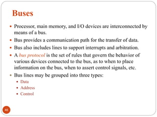
- 46. Buses Processor, main memory, and I/O devices are interconnected by means of a bus. Bus provides a communication path for the transfer of data. Bus also includes lines to support interrupts and arbitration. A bus protocol is the set of rules that govern the behavior of various devices connected to the bus, as to when to place information on the bus, when to assert control signals, etc. Bus lines may be grouped into three types: Data Address Control 46
- 47. Buses Control signals specify: Whether it is a read or a write operation. Required size of the data, when several operand sizes (byte, word, long word) are possible. Timing information to indicate when the processor and I/O devices may place data or receive data from the bus. Schemes for timing signals of data transfers over a bus can be classified into: Synchronous, Asynchronous. The Bus master is the device that initiates data transfer issuing read or write commands on the bus, hence it can be called as initiator. 47
- 48. Synchronous bus Bus cycle Data Bus clock command Address and t0 t1 t2 Time Master places the device address and command on the bus, and indicates that it is a Read operation. Addressed slave places data on the data lines Master “strobes” the data on the data lines into its input buffer, for a Read operation. In synchronous bus, all devices derive timing information from a common clock line. Equally spaced pulses on this line define equal time intervals. Each of these intervals constitutes a bus cycle during which one data transfer can take place. 48
- 49. Synchronous bus Consider the sequence of events during an read operation. At the time t0 , the master places the device address on the address lines and sends an appropriate command on the control lines. In this case, the command will indicate an input operation and specify the length of the operand to be read, if necessary. Information travels over the bus at the speed determined by its physical and electrical characteristics of the bus. Also, all the devices have to be given enough time to decode the address and control signals, so that the addressed slave can place data on the bus. Width of the pulse t1 - t0 depends on: Maximum propagation delay between two devices connected to the bus. Time taken by all the devices to decode the address and control signals, so that the 49
- 50. Synchronous bus At the end of the clock cycle, at time t2, the master strobes the data on the data lines into its input buffer if it’s a Read operation. “Strobe” means to capture the values of the data and store them into a buffer. When data are to be loaded into a storage buffer register, the data should be available for a period longer than the setup time of the device. Width of the pulse t2 - t1 should be longer than: Maximum propagation time of the bus plus Set up time of the input buffer register of the master. 50
- 51. Synchronous bus Data Bus clock command Address and t 0 t1 t 2 command Address and Data Seen by master Seen by slave tAM tAS tDS tDM Time • Signals do not appear on the bus as soon as they are placed on the bus, due to the propagation delay in the interface circuits. • Signals reach the devices after a propagation delay which depends on the characteristics of the bus. • Data must remain on the bus for some time after t2 equal to the hold time of the buffer. Address & command appear on the bus. Address & command reach the slave. Data appears on the bus. Data reaches the master. 51
- 52. Synchronous bus Limitations of traditional synchronous bus Data transfer has to be completed within one clock cycle. Clock period t2 - t0 must be such that the longest propagation delay on the bus and the slowest device interface must be accommodated. This forces all the devices to operate at the speed of the slowest device. Processor just assumes that the data are available at t2 in case of a Read operation, or are read by the device in case of a Write operation. Using Multiple-Cycle Transfers to overcome the above limitation Most buses have control signals to represent a response from the slave. Control signals serve two purposes: Inform the master that the slave has recognized the address, and is ready to participate in a data transfer operation. Enable to adjust the duration of the data transfer operation based on the speed of the participating slaves. High-frequency bus clock is used such that a complete data transfer cycle spans several clock cycles. 52
- 53. Synchronous bus 1 2 3 4 Clock Address Command Data Sla ve-ready Time Address & command requesting a Read operation appear on the bus. Slave places the data on the bus, and asserts Slave-ready signal. Master strobes data into the input buffer. Clock changes are seen by all the devices at the same time. 53
- 54. Asynchronous bus Data transfers on the bus is controlled by a handshake between the master and the slave. Common clock in the synchronous bus case is replaced by two timing control lines: Master-ready, Slave-ready. Master-ready signal is asserted by the master to indicate to the slave that it is ready to participate in a data transfer. Slave-ready signal is asserted by the slave in response to the master-ready from the master, and it indicates to the master that the slave is ready to participate in a data transfer. 54
- 55. Asynchronous bus Data transfer using the handshake protocol proceeds as follows: Master places the address and command information on the bus. Asserts the Master-ready signal to indicate to the slaves that the address and command information has been placed on the bus. All devices on the bus decode the address. Address slave performs the required operation, and informs the processor it has done so by asserting the Slave-ready signal. Master removes all the signals from the bus, once Slave-ready is asserted. If the operation is a Read operation, Master also strobes the data into its input buffer. 55
- 56. Asynchronous bus Slave-ready Data Master-ready and command Address Bus cycle t1 t2 t3 t4 t5 t0 Time t0 - Master places the address and command information on the bus. t1 - Master asserts the Master-ready signal. Master-ready signal is asserted at t1 instead of t0 t2 - Addressed slave places the data on the bus and asserts the Slave-ready signal. t3 - Slave-ready signal arrives at the master. t4 - Master removes the address and command information. t5 - Slave receives the transition of the Master-ready signal from 1 to 0. It removes the data and the Slave-ready signal from the bus. 56
- 57. Asynchronous bus Handshake control of data transfer during an output operation 57
- 58. Asynchronous bus Advantages of asynchronous bus: Eliminates the need for synchronization between the sender and the receiver. Can accommodate varying delays automatically, using the Slave-ready signal. Disadvantages of asynchronous bus: Data transfer rate with full handshake is limited by two-round trip delays. Data transfers using a synchronous bus involves only one round trip delay, and hence a synchronous bus can achieve faster rates. 58
- 59. Interface circuits An I/O interface consists of the circuitry required to connect an I/O device to a computer bus. One side of the interface which connects to the computer has bus signals for: Address, Data Control Other side of the interface which connects to the I/O device has: Datapath and associated controls to transfer data between the interface and the I/O device. This side is called as a “port”. Ports can be classified into two: Parallel port, Serial port. 59
- 60. Interface circuits Parallel port transfers data in the form of a number of bits, normally 8 or 16 to or from the device. Serial port transfers and receives data one bit at a time. Processor communicates with the bus in the same way, whether it is a parallel port or a serial port. I/O interface does the following: Provides a storage buffer for at least one word of data. Contains status flags that can be accessed by the processor to determine whether buffer is full (for input) or empty (for output). Contains address-decoding circuitry Generates the appropriate timing signals required by the bus control scheme. Performs any format conversion necessary to transfer data between bus and I/O device. 60
- 61. Parallel port- Keyboard to processor connection Valid Data Keyboard switches Encoder and debouncing circuit SIN Input interface Data Address R / Master -ready Sla ve-ready W DATAIN Processor • Keyboard is connected to a processor using a parallel port. • Processor is 32-bits and uses memory-mapped I/O and the asynchronous bus protocol. • On the processor side of the interface we have: - Data lines. - Address lines - Control or R/W line. - Master-ready signal and - Slave-ready signal. 61
- 62. Parallel port- Keyboard to processor connection • On the keyboard side of the interface: - A keyboard consists of mechanical switched that are normally open. - When a key is pressed, its switch closes and establishes a path for an electrical signal. - This signal is detected by Encoder circuit which generates a ASCII code for the key pressed. - Problem: Although a key bounce last only 1 or 2ms, this is long enough for the processor to observe single pressing of a key as several distinct electrical events. - Solution: Debouncing circuit which eliminates the effect of a key bounce. (I/O routine reads a character from the keyboard and waits long enough to ensure that bouncing has subsided. - The output of Encoder consists of encoded character and valid signal. - Valid line changes from 0 to 1 when the key is pressed. This causes the code to be loaded into DATAIN and SIN to be set to 1. 62
- 63. • Output lines of DATAIN are are connected to the data lines of the bus by means of 3 state drivers • Drivers are turned on when the processor issues a read signal and the address selects this register. • SIN signal is generated using a status flag circuit. • It is connected to line D0 of the processor bus using a three-state driver. • Address decoder selects the input interface based on bits A1 through A31. • Bit A0 determines whether the status or data register is to be read, when Master-ready is active. • In response, the processor activates the Slave-ready signal, when either the Read-status or Read-data is equal to 1, which depends on line A0. Input Interface Circuit
- 64. • Implementation of Status flag circuit Input Interface Circuit
- 65. Parallel port- Printer to processor connection CPU SOUT Output interface Data Address R / Master -ready Slave-ready Valid W Data DATAOUT Printer Processor Idle •Printer is connected to a processor using a parallel port. •Processor is 32 bits, uses memory-mapped I/O and asynchronous bus protocol. •On the processor side: - Data lines. - Address lines - Control or R/W line. - Master-ready signal and - Slave-ready signal. 65
- 66. Parallel port- Printer to processor connection •On the printer side: - The printer operates under control of handshake signals Valid and Idle. - The printer asserts its Idle signal when it is ready to accept a character. This causes the SOUT flag to be set to 1. - Processor places a new character into a DATAOUT register. - Valid signal, asserted by the interface circuit when it places a new character on the data lines. 66
- 67. • Data lines of the processor bus are connected to the DATAOUT register of the interface. • The status flag SOUT is connected to the data line D1 using a three- state driver. • The three-state driver is turned on, when the control Read-status line is 1. • Address decoder selects the output interface using address lines A1 through A31. • Address line A0 determines whether the data is to be loaded into the DATAOUT register or status flag is to be read. • If the Load-data line is 1, then the Valid line is set to 1. • If the Idle line is 1, then the status flag SOUT is set to 1. Output Interface Circuit
- 68. DATAIN 1 SIN Ready A31 A1 A0 Address decoder D7 D0 R/ W A2 DATAOUT Input status Bus PA7 PA0 CA PB7 PB0 CB1 CB2 SOUT D1 RS1 RS0 My-address Handshak e control Master - Ready Slave- Combined I/O interface circuit • Address bits A2 through A31, that is 30 bits are used to select the overall interface. • Address bits A1 through A0, that is, 2 bits select one of the three registers, namely, DATAIN, DATAOUT, and the status register. • Status register contains the flags SIN and SOUT in bits 0 and 1. • Data lines PA0 through PA7 connect the input device to the DATAIN register. • DATAOUT register connects the data lines on the processor bus to lines PB0 through PB7 which connect to the output device. • Separate input and output data lines for connection to an I/O device.
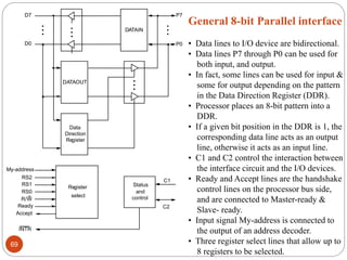
- 69. DATAIN DATAOUT Data Direction Re gister Register select Status and control Accept Ready R/W RS0 RS1 RS2 My-address INTR C1 C2 P7 P0 D7 D0 General 8-bit Parallel interface • Data lines to I/O device are bidirectional. • Data lines P7 through P0 can be used for both input, and output. • In fact, some lines can be used for input & some for output depending on the pattern in the Data Direction Register (DDR). • Processor places an 8-bit pattern into a DDR. • If a given bit position in the DDR is 1, the corresponding data line acts as an output line, otherwise it acts as an input line. • C1 and C2 control the interaction between the interface circuit and the I/O devices. • Ready and Accept lines are the handshake control lines on the processor bus side, and are connected to Master-ready & Slave- ready. • Input signal My-address is connected to the output of an address decoder. • Three register select lines that allow up to 8 registers to be selected. 69
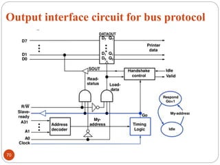
- 70. Output interface circuit for bus protocol 70
- 71. Timing signal for Output interface 71
- 72. Serial port Serial port is used to connect the processor to I/O devices that require transmission of data one bit at a time. Serial port communicates in a bit-serial fashion on the device side and bit parallel fashion on the bus side. Transformation between the parallel and serial formats is achieved with shift registers that have parallel access capability. 72
- 73. I NTR Chip and register select Status and control Accept Ready R/W RS0 RS1 My-address Recei ving clock T ransmission clock D7 D0 Output shift re gister DATAOUT DATAIN Input shift re gister Serial Serial input • Input shift register accepts input one bit at a time from the I/O device. • Once all the 8 bits are received, the contents of the input shift register are loaded in parallel into DATAIN register. • Output data in the DATAOUT register are loaded into the output shift register. • Bits are shifted out of the output shift register and sent out to the I/O device one bit at a time. • As soon as data from the input shift reg. are loaded into DATAIN, it can start accepting another 8 bits of data. • Input shift register and DATAIN registers are both used at input so that the input shift register can start receiving another set of 8 bits from the input device after loading the contents to DATAIN, before the processor reads the contents of DATAIN. This is called as double-buffering. 73
- 74. Serial port Serial interfaces require fewer wires, and hence serial transmission is convenient for connecting devices that are physically distant from the computer. Speed of transmission of the data over a serial interface is known as the “bit rate”. Bit rate depends on the nature of the devices connected. In order to accommodate devices with a range of speeds, a serial interface must be able to use a range of clock speeds. Several standard serial interfaces have been developed: Universal Asynchronous Receiver Transmitter (UART) for low-speed serial devices. RS-232-C for connection to communication links. 74
- 75. Standard I/O interfaces I/O device is connected to a computer using an interface circuit. Do we have to design a different interface for every combination of an I/O device and a computer? A practical approach is to develop standard interfaces and protocols. A personal computer has: A motherboard which houses the processor chip, main memory and some I/O interfaces. A few connectors into which additional interfaces can be plugged. Processor bus is defined by the signals on the processor chip. Devices which require high-speed connection to the processor are connected directly to this bus. 75
- 76. Standard I/O interfaces Because of electrical reasons only a few devices can be connected directly to the processor bus. Motherboard usually provides another bus that can support more devices. Processor bus and the other bus (called as expansion bus) are interconnected by a circuit called “bridge”. Devices connected to the expansion bus experience a small delay in data transfers. Design of a processor bus is closely tied to the architecture of the processor. No uniform standard can be defined. Expansion bus however can have uniform standard defined. 76
- 77. Standard I/O interfaces 77 A number of standards have been developed for the expansion bus. Some have evolved by default. For example, IBM’s Industry Standard Architecture. Three widely used bus standards: PCI (Peripheral Component Interconnect) SCSI (Small Computer System Interface) USB (Universal Serial Bus)
- 78. Standard I/O interfaces Main memory Processor Bridge Processor bus PCI bus memory Additional controller CD-ROM controller Disk Disk 1 Disk 2 ROM CD- SCSI controller USB controller Video Ke yboard Game disk IDE SCSI b us ISA Ethernet Interface Expansion bus on the motherboard Bridge circuit translates signals and protocols from processor bus to PCI bus. Interface 78
- 79. Peripheral Component Interconnect (PCI) Bus Introduced in 1992 Low-cost bus Processor independent Plug-and-play capability In today’s computers, most memory transfers involve a burst of data rather than just one word. The PCI is designed primarily to support this mode of operation. The bus supports three independent address spaces: memory, I/O, and configuration. we assumed that the master maintains the address information on the bus until data transfer is completed. But, the address is needed only long enough for the slave to be selected. Thus, the address is needed on the bus for one clock cycle only, freeing the address lines to be used for sending data in subsequent clock cycles. The result is a significant cost reduction. A master is called an initiator in PCI terminology. The addressed device that responds to read and write commands is called a target. 79
- 80. Peripheral Component Interconnect (PCI) Bus Use of PCI bus in a computer system 80
- 81. Peripheral Component Interconnect (PCI) Bus Data transfer signals on the PCI bus 81
- 82. 1 2 3 4 5 6 7 CLK Frame# AD C/BE# IRDY# TRDY# DEVSEL# Adress #1 #4 Cmnd Byte enable A read operation on the PCI bus #2 #3 82
- 83. Device Configuration When an I/O device is connected to a computer, several actions are needed to configure both the device and the software that communicates with it. PCI incorporates in each I/O device interface a small configuration ROM memory that stores information about that device. The configuration ROMs of all devices are accessible in the configuration address space. The PCI initialization software reads these ROMs and determines whether the device is a printer, a keyboard, an Ethernet interface, or a disk controller. It can further learn bout various device options and characteristics. Devices are assigned addresses during the initialization process. This means that during the bus configuration operation, devices cannot be accessed based on their address, as they have not yet been assigned one. Hence, the configuration address space uses a different mechanism. Each device has an input signal called Initialization Device Select, IDSEL# Electrical characteristics: PCI bus has been defined for operation with either a 5 or 3.3 V power supply 83
- 84. SCSI Bus The acronym SCSI stands for Small Computer System Interface. It refers to a standard bus defined by the American National Standards Institute (ANSI) under the designation X3.131 . In the original specifications of the standard, devices such as disks are connected to a computer via a 50-wire cable, which can be up to 25 meters in length and can transfer data at rates up to 5 megabytes/s. The SCSI bus standard has undergone many revisions, and its data transfer capability has increased very rapidly, almost doubling every two years. SCSI-2 and SCSI-3 have been defined, and each has several options. Because of various options SCSI connector may have 50, 68 or 80 pins. 84
- 85. SCSI Bus Devices connected to the SCSI bus are not part of the address space of the processor The SCSI bus is connected to the processor bus through a SCSI controller. This controller uses DMA to transfer data packets from the main memory to the device, or vice versa. A packet may contain a block of data, commands from the processor to the device, or status information about the device. A controller connected to a SCSI bus is one of two types – an initiator or a target. An initiator has the ability to select a particular target and to send commands specifying the operations to be performed. The disk controller operates as a target. It carries out the commands it receives from the initiator. The initiator establishes a logical connection with the intended target. Once this connection has been established, it can be suspended and restored as needed to transfer commands and bursts of data. 85
- 86. SCSI Bus While a particular connection is suspended, other device can use the bus to transfer information. This ability to overlap data transfer requests is one of the key features of the SCSI bus that leads to its high performance. Data transfers on the SCSI bus are always controlled by the target controller. To send a command to a target, an initiator requests control of the bus and, after winning arbitration, selects the controller it wants to communicate with and hands control of the bus over to it. Then the controller starts a data transfer operation to receive a command from the initiator. 86
- 87. SCSI Bus Assume that processor needs to read block of data from a disk drive and that data are stored in disk sectors that are not contiguous. The processor sends a command to the SCSI controller, which causes the following sequence of events to take place: 1. The SCSI controller, acting as an initiator, contends for control of the bus. 2. When the initiator wins the arbitration process, it selects the target controller and hands over control of the bus to it. 3. The target starts an output operation (from initiator to target); in response to this, the initiator sends a command specifying the required read operation. 4. The target, realizing that it first needs to perform a disk seek operation, sends a message to the initiator indicating that it will temporarily suspend the connection between them. Then it releases the bus. 5. The target controller sends a command to the disk drive to move the read head to the first sector involved in the requested read operation. Then, it reads the data stored in that sector and stores them in a data buffer. When it is ready to begin transferring data to the initiator, the target requests control of the bus. After it wins arbitration, it reselects the initiator controller, thus restoring the suspended connection. 87
- 88. SCSI Bus 6. The target transfers the contents of the data buffer to the initiator and then suspends the connection again 7. The target controller sends a command to the disk drive to perform another seek operation. Then, it transfers the contents of the second disk sector to the initiator as before. At the end of this transfers, the logical connection between the two controllers is terminated. 8. As the initiator controller receives the data, it stores them into the main memory using the DMA approach. 9. The SCSI controller sends as interrupt to the processor to inform it that the requested operation has been completed 88
- 89. Table 4. The SCSI bus signals. Operation of SCSI bus from H/W point of view 89
- 90. Main Phases involved in operation of SCSI bus Arbitration A controller requests the bus by asserting BSY and by asserting it’s associated data line When BSY becomes active, all controllers that are requesting bus examine data lines Selection Controller that won arbitration selects target by asserting SEL and data line of target. After that initiator releases BSY line. Target responds by asserting BSY line Target controller will have control on the bus from then Information Transfer Handshaking signals are used between initiator and target At the end target releases BSY line Reselection When logical connection is suspended and target is ready to restore, the target must first gain control of the bus It starts an arbitration cycle, after winning arbitration, it selects the initiator controller 90
- 91. Free Arbitration Selection Targets examine ID DB 2 DB 5 DB 6 BSY SEL Figure 42. Arbitration and selection on the SCSI bus. Device 6 wins arbitration and selects device 2. 91
- 92. Universal Serial Bus (USB) USB is an industry standard developed through a collaborative effort of several computer and communication companies, including Compaq, Hewlett-Packard, Intel, Lucent, Microsoft, Nortel Networks, and Philips. Speed Low-speed(1.5 Mb/s) Full-speed(12 Mb/s) High-speed(480 Mb/s) Port Limitation Device Characteristics - Asynchronous - Isochronous Plug-and-play 92
- 93. Host computer Root hub Hub I/O device Hub I/O device I/O device Hub I/O device I/O device I/O device Universal Serial Bus tree structure 93
- 94. Universal Serial Bus tree structure Each node of the tree has a device called a hub, which acts as an intermediate control point between the host and the I/O devices. At the root of the tree, a root hub connects the entire tree to the host computer. The leaves of the tree are the I/O devices being served (for example, keyboard, Internet connection, speaker, or digital TV) In normal operation, a hub copies a message that it receives from its upstream connection to all its downstream ports. As a result, a message sent by the host computer is broadcast to all I/O devices, but only the addressed device will respond to that message. However, a message from an I/O device is sent only upstream towards the root of the tree and is not seen by other devices. Hence, the USB enables the host to communicate with the I/O devices, but it does not enable these devices to communicate with each other. 94
- 95. USB- Addressing When a USB is connected to a host computer, its root hub is attached to the processor bus, where it appears as a single device. The host software communicates with individual devices attached to the USB by sending packets of information, which the root hub forwards to the appropriate device in the USB tree. Each device on the USB, whether it is a hub or an I/O device, is assigned a 7-bit address. This address is local to the USB tree and is not related in any way to the addresses used on the processor bus. A hub may have any number of devices or other hubs connected to it, and addresses are assigned arbitrarily. When a device is first connected to a hub, or when it is powered on, it has the address 0. 95
- 96. USB- Addressing When a device is first connected to a hub, or when it is powered on, it has the address 0. The hardware of the hub to which this device is connected is capable of detecting that the device has been connected, and it records this fact as part of its own status information. Periodically, the host polls each hub to collect status information and learn about new devices that may have been added or disconnected. When the host is informed that a new device has been connected, it uses a sequence of commands to send a reset signal on the corresponding hub port, read information from the device about its capabilities, send configuration information to the device, and assign the device a unique USB address. Once this sequence is completed the device begins normal operation and responds only to the new address. 96
- 97. USB Protocols All information transferred over the USB is organized in packets, where a packet consists of one or more bytes of information. There are many types of packets that perform a variety of control functions. The information transferred on the USB can be divided into two broad categories: control and data. Control packets perform such tasks as addressing a device to initiate data transfer, acknowledging that data have been received correctly, or indicating an error. Data packets carry information that is delivered to a device. A packet consists of one or more fields containing different kinds of information. The first field of any packet is called the packet identifier, PID, which identifies the type of that packet. They are transmitted twice. The first time they are sent with their true values, and the second time with each bit complemented The four PID bits identify one of 16 different packet types. Some control packets, such as ACK (Acknowledge), consist only of the PID byte. 97
- 98. PID0 PID1 PID2 PID3 PID0 PID0 PID1 PID2 PID3 (a) Packet identifier field PID ADDR ENDP CRC16 8 7 4 5 Bits (b) Token packet, IN or OUT PID DATA CRC16 8 0 to 8192 16 Bits (c) Data packet USB packet format. Control packets used for controlling data transfer operations are called token packets. 98
- 99. Figure: An output transfer ACK Tok en Data0 Tok en Data1 Host Hub I/O De vice Tok en Data0 ACK ACK Tok en Data1 ACK Time 99
- 100. Isochronous Traffic on USB One of the key objectives of the USB is to support the transfer of isochronous data. Devices that generates or receives isochronous data require a time reference to control the sampling process. To provide this reference. Transmission over the USB is divided into frames of equal length. A frame is 1ms long for low-and full-speed data. The root hub generates a Start of Frame control packet (SOF) precisely once every 1 ms to mark the beginning of a new frame. The arrival of an SOF packet at any device constitutes a regular clock signal that the device can use for its own purposes. To assist devices that may need longer periods of time, the SOF packet carries an 11-bit frame number. Following each SOF packet, the host carries out input and output transfers for isochronous devices. This means that each device will have an opportunity for an input or output transfer once every 1 ms. 100
- 101. Electrical Characteristics The cables used for USB connections consist of four wires. Two are used to carry power, +5V and Ground. Thus, a hub or an I/O device may be powered directly from the bus, or it may have its own external power connection. The other two wires are used to carry data. Different signaling schemes are used for different speeds of transmission. At low speed, 1s and 0s are transmitted by sending a high voltage state (5V) on one or the other o the two signal wires. For high-speed links, differential transmission is used. 101
- 102. Model Questions 1. In a situation where multiple devices capable of initiating interrupts are connected to processor, explain the implementation of interrupt priority, using individual INTER and INTA and a common INTR line to all devices. 2. Define the terms 'cycle stealing' and 'block mode'. 3. What is bus arbitration ? Explain the different approaches to bus arbitration. 4. Briefly discuss the main phases involved in the operation of SCSI bus. 5. Explain the tree structure of USB with split bus operation. 6. Explain the following terms I) interrupt service routine II) interrupt latency III)interrupt disabling 7. With a diagram explain daisy chaining technique 8. With a block diagram explain how the printer is interfaced to processor 9. Define two types of SCSI controller. 10. Explain the use of PCI bus in a computer with necessary figure. 11. List the SCSI bus signals with their functions. 102
- 103. Model Questions 12. Define memory mapped IO and IO mapped IO with examples. 13. What are the different methods of DMA? Explain them in brief. Explain the registers in DMA. 14. Explain the serial port and serial interface. 15. What is an interrupt? with example illustrate the concept of interrupts. Explain polling and vectored interrupts. 16. Describe how a read operation is performed on a PCI bus. 17. List the sequence of events that takes place when a processor sends a commands to the SCSI controller. 18. Define exceptions. Explain two kinds of exceptions 19. Draw and explain the general 8 bit parallel processing. 20. Explain the following with respect to USB, I) USB architecture, II) USB addressing, III) USB protocols. 21. List out the functions of an IO interface. 103