

![SFRs associated with Timers
• TMOD [Timer mode]
8 bit register
Used for selecting the operating modes of T0 and T1
As shown in figure, the low 4 bits (bit0 – bit3) refer to the timer 0,
while the high 4 bits (bit4 – bit7) refer to the timer 1.
• GATE1 enables and disables Timer 1 by means of a signal brought
to the INT1 pin (P3.3)- external triggering
• 1 – Timer 1 operates only if the INT1 bit is set.
• 0 – Timer 1 operates regardless of the logic state of the INT1 bit.
Timer 1 Timer 0](https://image.slidesharecdn.com/495053119eet303module5-241231173251-4df71540/85/KTU_Microprocessor-and-Microcontrollers_Module2-4-320.jpg)


![• Timer 0 in mode 0 [ 13 bit timer/counter]
This is one of the varities being kept only for the purpose of
compatibility with the previous versions of microcontrollers.
This mode configures timer 0 as a 13-bit timer which consists of
all 8 bits of TH0 and the lower 5 bits of TL0.
As a result, the Timer 0 uses only 13 of 16 bits.
Each coming pulse causes the timer register bits to change their
states.
This process is repeated until registers count up 8192 pulses.
After that, both registers are cleared and counting starts from 0.
• Timer 0 in mode 1 (16-bit timer)
Mode 1 configures timer 0 as a 16-bit timer comprising all the
bits of both registers TH0 and TL0.
Timer operates in the same way as in mode 0, with difference
that the registers count up to 65 536 as allowable by the 16 bits.](https://image.slidesharecdn.com/495053119eet303module5-241231173251-4df71540/85/KTU_Microprocessor-and-Microcontrollers_Module2-7-320.jpg)


![• Program for generating 1mS delay using 8051 timer working
with 12MHz crystal. Use Timer 0
Set Timer/Counter module 0 as timer using TMOD register
Set timer in Mode 1(16 bit timer)
5ms = 5000micro s >>> Count = 65536-5000 = 60536
Convert into Hex >>. 64536 = FC 18H
Load in Timer Registers [TH/TL] >> TH0=FC,TL0=18
Start Timer, wait
Stop Timer and clear flags
MOV TMOD,#00000001B
MOV TH0,#0FCH
MOV TL0,#18H
SETB TR0
HERE: JNB TF0,HERE
CLR TR0
CLR TF0
Void delay ()
{
TMOD = 0x01;
TH0= 0xFC;
TL0 = 0x18;
TR0 = 1;
while (TF0 == 0);
TR0 = 0;
TF0 = 0;
}](https://image.slidesharecdn.com/495053119eet303module5-241231173251-4df71540/85/KTU_Microprocessor-and-Microcontrollers_Module2-10-320.jpg)


![• SFR Associated with interrupts
1. IE [ Interrupt Enable]
Used to enable and disable 5 interrupt sources individually or
together
EA – global interrupt enable/disable:
• 0 – disables all interrupt requests.
• 1 – enables all individual interrupt requests.
ES – enables or disables serial interrupt:
• 0 – UART system cannot generate an interrupt.
• 1 – UART system enables an interrupt.](https://image.slidesharecdn.com/495053119eet303module5-241231173251-4df71540/85/KTU_Microprocessor-and-Microcontrollers_Module2-33-320.jpg)


![• External Interrupt Programming
Pressing a switch will turn on LED
Vector Address = 0013H[ ISR must be loaded here]
Enabling external interrupt 1 with highest priorities [ IE and IP
register bits will be used, falling edge ]](https://image.slidesharecdn.com/495053119eet303module5-241231173251-4df71540/85/KTU_Microprocessor-and-Microcontrollers_Module2-49-320.jpg)

KTU_Microprocessor and Microcontrollers_Module2
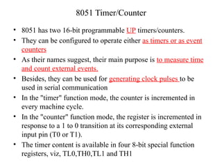
- 1. • Timer Applications Examples Turning ON LED for 1 second and turn off. Shutting down a devise after 30 minutes. Transmitting Message with intervals When Interfacing devices like LCD • Counter Applications Taking the count of persons entering to a room. Automatic Parking Bay Smart Meters • Timer and Counter Together Digital Tachometers (RPM)
- 2. 8051 Timer/Counter • 8051 has two 16-bit programmable UP timers/counters. • They can be configured to operate either as timers or as event counters • As their names suggest, their main purpose is to measure time and count external events. • Besides, they can be used for generating clock pulses to be used in serial communication • In the "timer" function mode, the counter is incremented in every machine cycle. • In the "counter" function mode, the register is incremented in response to a 1 to 0 transition at its corresponding external input pin (T0 or T1). • The timer content is available in four 8-bit special function registers, viz, TL0,TH0,TL1 and TH1
- 3. • Timer/Counter 0 • Since the timer T0 is virtually 16-bit register, the largest value it can store is 65 535. • In case of exceeding this value, the timer will be automatically cleared and counting starts from 0. • This condition is called an overflow – will generate interrupt
- 4. SFRs associated with Timers • TMOD [Timer mode] 8 bit register Used for selecting the operating modes of T0 and T1 As shown in figure, the low 4 bits (bit0 – bit3) refer to the timer 0, while the high 4 bits (bit4 – bit7) refer to the timer 1. • GATE1 enables and disables Timer 1 by means of a signal brought to the INT1 pin (P3.3)- external triggering • 1 – Timer 1 operates only if the INT1 bit is set. • 0 – Timer 1 operates regardless of the logic state of the INT1 bit. Timer 1 Timer 0
- 5. • C/T1 selects pulses to be counted up by the timer/counter 1: • 1 – Timer counts pulses brought to the T1 pin (P3.5) – will work as counter • 0 – Timer counts pulses from internal oscillator – will work as timer • T1M1,T1M0 These two bits select the operational mode of the Timer 1. T1M1 T1M0 MODE DESCRIPTION 0 0 0 13-bit timer 0 1 1 16-bit timer 1 0 2 8-bit auto-reload 1 1 3 Split mode
- 6. • GATE 0 enables and disables Timer 1 by means of a signal brought to the INT 0 pin (P3.2)- external triggering • 1 – Timer 0 operates only if the INT0 bit is set. • 0 – Timer 0 operates regardless of the logic state of the INT0 bit. • C/T0 selects pulses to be counted up by the timer/counter 0: • 1 – Timer counts pulses brought to the T0 pin (P3.4) – will work as counter • 0 – Timer counts pulses from internal oscillator – will work as timer • T0M1,T0M0 These two bits select the operational mode of the Timer 0.
- 7. • Timer 0 in mode 0 [ 13 bit timer/counter] This is one of the varities being kept only for the purpose of compatibility with the previous versions of microcontrollers. This mode configures timer 0 as a 13-bit timer which consists of all 8 bits of TH0 and the lower 5 bits of TL0. As a result, the Timer 0 uses only 13 of 16 bits. Each coming pulse causes the timer register bits to change their states. This process is repeated until registers count up 8192 pulses. After that, both registers are cleared and counting starts from 0. • Timer 0 in mode 1 (16-bit timer) Mode 1 configures timer 0 as a 16-bit timer comprising all the bits of both registers TH0 and TL0. Timer operates in the same way as in mode 0, with difference that the registers count up to 65 536 as allowable by the 16 bits.
- 8. • Timer 0 in mode 2 (Auto-Reload Timer) Mode 2 configures timer 0 as an 8-bit timer. Actually, timer 0 uses only one 8-bit register for counting and never counts from 0, but from an arbitrary value (0-255) stored in another (TH0) register When the TL0 register overflows instead of being cleared, the contents of TH0 will be reloaded to it. • Timer 0 in Mode 3 (Split Timer) Mode 3 configures timer 0 so that registers TL0 and TH0 operate as separate 8-bit timers. In other words, the 16-bit timer consisting of two registers TH0 and TL0 is split into two independent 8-bit timers.
- 9. • TCON Register TCON register is also one of the registers whose bits are directly in control of timer operation. Only 4 bits of this register are used for this purpose, while rest of them is used for external interrupt control • TF1 bit is automatically set on the Timer 1 overflow. • TR1 bit enables the Timer 1. 1 – Timer 1 is enabled. 0 – Timer 1 is disabled. • TF0 bit is automatically set on the Timer 0 overflow. • TR0 bit enables the timer 0. 1 – Timer 0 is enabled. 0 – Timer 0 is disabled.
- 10. • Program for generating 1mS delay using 8051 timer working with 12MHz crystal. Use Timer 0 Set Timer/Counter module 0 as timer using TMOD register Set timer in Mode 1(16 bit timer) 5ms = 5000micro s >>> Count = 65536-5000 = 60536 Convert into Hex >>. 64536 = FC 18H Load in Timer Registers [TH/TL] >> TH0=FC,TL0=18 Start Timer, wait Stop Timer and clear flags MOV TMOD,#00000001B MOV TH0,#0FCH MOV TL0,#18H SETB TR0 HERE: JNB TF0,HERE CLR TR0 CLR TF0 Void delay () { TMOD = 0x01; TH0= 0xFC; TL0 = 0x18; TR0 = 1; while (TF0 == 0); TR0 = 0; TF0 = 0; }
- 11. 8051Serial Communication • Basics of Serial Communication
- 12. • 8051 Serial Communication Byte of data must be converted to serial bits using a parallel-in- serial-out shift register and transmitted over a single data line At receiving end there must be a serial-in-parallel-out shift register If transferred on the telephone line, it must be converted to audio tones by modem For short distance the signal can be transferred using wire 2 methods, asynchronous and synchronous • Synchronous method transfers a block of data (characters) at a time • Asynchronous method transfers a single byte at a time Eg : USB,CAN,RS-232,
- 13. • Different Types of Transmission
- 14. • In simplex transmissions, the computer can only send data. There is only one wire. • If the data can be transmitted and received, then it is a duplex transmission • Duplex transmissions can be half or full duplex depending on whether or not the data transfer can be simultaneous. • If the communication is only one way at a time, it is half duplex • If both sides can communicate at the same time, it is full duplex • Full duplex requires two wire conductors for the data lines (in addition to the signal ground)
- 15. • Serial Communication can be Asynchronous Synchronous • Synchronous Communication Synchronous methods transfer a block of data (characters) at a time The events are referenced to a clock Example: SPI bus, I2C bus • Asynchronous Communication Asynchronous methods transfer a single byte at a time There is no clock. The bytes are separated by start and stop bits. Example: UART • The microcontrollers use special IC chips called UART (universal asynchronous receiver-transmitter) and USART (universal synchronous asynchronous receiver-transmitter) 8051 chip has a built-in UART
- 16. • Baud Rate The rate of data transfer in serial data communication is stated in bps (bits per second) Another widely used terminology for bps is baud rate, It is modem terminology and is defined as the number of signal changes per second. As far as the conductor wire is concerned, the baud rate and bps are the same, and we use the terms interchangeably. • Setting Baud Rate in 8051 Baud rate in the 8051 baud rate in the 8051 is programmable 8051 divides the crystal frequency by 12 to get the machine cycle frequency. UART divides the machine cycle frequency by 32 once more before it is used by Timer 1 to set the baud rate Timer 1 must be programmed in mode 2, that is 8-bit, auto- reload
- 17. • Example : Baud Rate = 9600 1. Crystal Frequency = 11.0592 (12MHz) 2. Divide by 12 = 921.6KHz 3. Divide by 32 = 28800Hz 4. Value = 28800/BR (28800/9600 = 3) 5. TH1 = 256 – Value = 253 6. Convert to Hex TH1 = FDH 7. Timer 1 must be programmed in mode 2, that is 8-bit, auto- reload
- 18. • SCON Register SCON is an 8-bit register used to program the start bit, stop bit, and data bits of data framing, among other Things SM0 : Serial Mode Specifier SM1 : Serial Mode Speceifier SM2 : Used for multiprocessor Communication REN : Set/Cleared by Software to enable/disable reception TB8 : not used in Mode 1 RB8 : Not used in Mode 1 TI : Transmit interrupt flag. Set by HW at the begin of the stop bit mode 1. And cleared by SW RI : Receive interrupt flag. Set by HW at the begin of the stop bit mode 1. And cleared by SW SM0 SM1 SM2 REN TB8 RB8 TI RI
- 19. • SM0, SM1 determine the framing of data by specifying the number of bits per character, and the start and stop bits
- 20. • Mode 0 In this mode, the serial port works like a shift register and the data transmission works synchronously with a clock frequency of fosc /12. Serial data is received and transmitted through RXD/RXD 8 bits are transmitted/ received at a time. Pin TXD outputs the shift clock pulses of frequency fosc /12, which is connected to the external circuitry for synchronization. The shift frequency or baud rate is always 1/12 of the oscillator frequency. • Mode 1 In mode-1, the serial port functions as a standard Universal Asynchronous Receiver Transmitter (UART) mode. 10 bits are transmitted through TXD or received through RXD. The 10 bits consist of one start bit (which is usually '0'), 8 data bits (LSB is sent first/received first), and a stop bit (which is usually '1').
- 21. Once received, the stop bit goes into RB8 in the special function register SCON. The baud rate is variable. • Mode 2 In this mode 11 bits are transmitted through TXD or received through RXD. The various bits are as follows: a start bit (usually '0'), 8 data bits (LSB first), a programmable 9 th (TB8 or RB8)bit and a stop bit (usually '1').While transmitting, the 9 th data bit (TB8 in SCON) can be assigned the value '0' or '1‘. • For example, if the information of parity is to be transmitted, the parity bit (P) in PSW could be moved into TB8. On reception of the data, the 9 th bit goes into RB8 in 'SCON', while the stop bit is ignored. The baud rate is programmable to either 1/32 or 1/64 of the oscillator frequency.
- 22. • Mode 3 In this mode 11 bits are transmitted through TXD or received through RXD. The various bits are: a start bit (usually '0'), 8 data bits (LSB first), a programmable 9 th bit and a stop bit (usually '1'). Mode-3 is same as mode-2, except the fact that the baud rate in mode-3 is variable (i.e., just as in mode-1). f baud = (2^SMOD /32) * ( fosc / 12 (256-TH1)) . This baud rate holds when Timer-1 is programmed in Mode-2. SM0 SM1 Mode Description Baud Rate 0 0 Mode 0 8 bit Shift Register mode 0 1 Mode 1 8 bit UART Variable 1 0 Mode 2 9 bit UART or 1 1 Mode 3 9 bit UART Variable
- 23. • SBUF Register The special function register SBUF is physically two registers. • One is, write-only and is used to hold data to be transmitted out of the 8051 via TXD. • The other is, read-only and holds the received data from external sources via RXD. Both mutually exclusive registers have the same address 099H. SBUF is not bit addressable • Programming the 8051 to transfer character bytes serially 1. Set Timer 1 in Mode 2. So TMOD = 20H 0 0 1 0 0 0 0 0 GATE 1 C/T1 T1M1 T1M0 GATE0 C/T0 T0M1 T0M0 TMOD = 20H
- 24. 1. The TH1 is loaded with one of the value to set baud rate for serial data transfer 2. The SCON register is loaded with the value 50H, indicating serial mode 1, where an 8- bit data is framed with start and stop bits 4. TR1 is set to 1 to start timer 1 5. TI is cleared by CLR TI instruction 6. The character byte to be transferred serially is written into SBUF register 7. The TI flag bit is monitored with the use of instruction JNB TI, xx to see if the character has been transferred completely. 8. To transfer the next byte, go to step 5 0 1 0 1 0 0 0 0 SM0 SM1 SM2 REN TB8 RB8 TI RI SCON = 50H
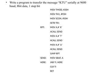
- 25. • Write a program to transfer the message “KTU” serially at 9600 baud, 8bit data, 1 stop bit MOV TMOD, #20H MOV TH1, #FDH MOV SCON, #50H SETB TR1 RPT: MOV A,# ‘K’ ACALL SEND MOV A,# ‘T’ ACALL SEND MOV A,# ‘U’ ACALL SEND SJMP RPT SEND: MOV SBUF, A HERE: JNB TI, HERE CLR TI RET
- 26. void main { TMOD = 0x20; TH1 = 0xFA; SCON = 0x50; TR1 = 1; while(1) { SBUF = ‘A’; while(TI ==0); TI = 0; } } • C program to transmit letter ‘A’ continuously with 4800 baud rate.
- 27. • C program to transmit message ‘KTU’ continuously with 9600 baud rate. void main { TMOD = 0x20; TH1 = 0xFD; SCON = 0x50; TR1 = 1; while(1) { Msg_Tx(‘K’); Msg_Tx(‘T’); Msg_Tx(‘U’); } } void Msg_Tx(unsigned char x) { SBUF = x; while TI = 0; TI = 0; }
- 28. 8051 Interrupts • In most of the real-time processes, to handle certain conditions properly, the actual task must be halt for some time – it takes required action – and then must return to the main task. • For executing such type of programs, interrupts are necessary. • It entirely differs from the polling method wherein the processor must check sequentially each device and ask whether the service is required or not while consuming more processor time. • Interrupts in 8051 microcontroller are more desirable to reduce the regular status checking of the interfaced devices or inbuilt devices. • Interrupt is an event that temporarily suspends the main program, passes the control to a special code section, executes the event-related function and resumes the main program flow where it had left off.
- 29. • Types of interrupts Maskable and Non maskable Hardware and Software Fixed and Vectored • Types of Interrupts in 8051 Microcontroller The 8051 microcontroller can recognize five different events that cause the main program to interrupt from the normal execution. These five sources of interrupts in 8051are: 1. Timer 0 overflow interrupt- TF0 2. Timer 1 overflow interrupt- TF1 3. External hardware interrupt- INT0 4. External hardware interrupt- INT1 5. Serial communication interrupt- RI/TI
- 30. • The Timer and Serial interrupts are internally generated by the microcontroller, whereas the external interrupts are generated by additional interfacing devices(sensors) or switches that are externally connected to the microcontroller. • These external interrupts can be edge triggered or level triggered. • When an interrupt occurs, the microcontroller executes the interrupt service routine so that memory location corresponds to the interrupt that enables it. • The Interrupt corresponding to the memory location is given in the interrupt vector table below. Interrupt Description Vector Address External Interrupt 0 0003H Timer/Counter 0 000BH External Interrupt 1 0013H Timer/Counter 1 001BH Serial Port 0023H
- 31. • Interrupt Structure 0f 8051 There are five interrupt sources for the 8051, which means that they can recognize 5 different events that can interrupt regular program execution. Each interrupt can be enabled or disabled by setting bits of the IE register. Likewise, the whole interrupt system can be disabled by clearing the EA bit of the same register. If the IT0 and IT1 bits of the TCON register are set, an interrupt will be generated on high to low transition, i.e. on the falling pulse edge (only in that moment). – Edge Triggered If these bits are cleared, an interrupt will be continuously executed as far as the pins are held low. – Level Triggered
- 33. • SFR Associated with interrupts 1. IE [ Interrupt Enable] Used to enable and disable 5 interrupt sources individually or together EA – global interrupt enable/disable: • 0 – disables all interrupt requests. • 1 – enables all individual interrupt requests. ES – enables or disables serial interrupt: • 0 – UART system cannot generate an interrupt. • 1 – UART system enables an interrupt.
- 34. ET1 – bit enables or disables Timer 1 interrupt: • 0 – Timer 1 cannot generate an interrupt. • 1 – Timer 1 enables an interrupt. EX1 – bit enables or disables external 1 interrupt: • 0 – change of the pin INT0 logic state cannot generate an interrupt. • 1 – enables an external interrupt on the pin INT0 state change. ET0 – bit enables or disables timer 0 interrupt: • 0 – Timer 0 cannot generate an interrupt. • 1 – enables timer 0 interrupt. EX0 – bit enables or disables external 0 interrupt: • 0 – change of the INT1 pin logic state cannot generate an interrupt. • 1 – enables an external interrupt on the pin INT1 state change.
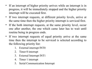
- 35. • Interrupt Priorities It is not possible to forseen when an interrupt request will arrive. If several interrupts are enabled, it may happen that while one of them is in progress, another one is requested. In order that the microcontroller knows whether to continue operation or meet a new interrupt request, there is a priority list instructing it what to do. The priority list offers 3 levels of interrupt priority: • Reset- When a reset request arrives, everything is stopped and the microcontroller restarts. • Interrupt priority 1 can be disabled by Reset only. • Interrupt priority 0 can be disabled by both Reset and interrupt priority 1. The IP Register (Interrupt Priority Register) specifies which one of existing interrupt sources have higher and which one has lower priority. Interrupt priority is usually specified at the beginning of the program.
- 36. • If an interrupt of higher priority arrives while an interrupt is in progress, it will be immediately stopped and the higher priority interrupt will be executed first. • If two interrupt requests, at different priority levels, arrive at the same time then the higher priority interrupt is serviced first. • If the both interrupt requests, at the same priority level, occur one after another, the one which came later has to wait until routine being in progress ends. • If two interrupt requests of equal priority arrive at the same time then the interrupt to be serviced is selected according to the following priority list: 1. External interrupt INT0 2. Timer 0 interrupt 3. External Interrupt INT1 4. Timer 1 interrupt 5. Serial Communication Interrupt
- 37. ADC Interfacing An analog to digital converter or ADC, as the name suggests, converts an analog signal to a digital signal. An ADC maps analog signals to their binary equivalents. This minimum change that an ADC can detect is known as the step size of the ADC. Eg: Vmax = 5V, Vmin = 0V, 8 bit ADC Step Size = 5/2^8 = 5/256 = 19.53mV ADC 0808 – 8 bit ADC Step size = Vmax - Vmin/2n (where n is the number of bits(resolution) of an ADC)
- 38. • ADC 0808
- 39. Input pins (INT0-INT7) • The ADC 0808 has eight input analog pins. • These pins are multiplexed together, and only one of them can be selected using three select lines. Select lines • It has three select lines, namely A, B, and C, that are used to select the desired input lines. A B C Input 0 0 0 INT 0 0 0 1 INT 1 0 1 0 INT 2 0 1 1 INT 3 1 0 0 INT 4 1 0 1 INT 5 1 1 0 INT 6 1 1 1 INT 7
- 40. ALE – Low to High pulse VREF (+) and VREF (-) • These two pins are used to provide the upper and the lower limit of voltages which determine the step size for the conversion. Start conversion • This pin is used to tell the ADC to start the conversion. • When the ADC receives a low to high pulse on this pin, it starts converting the analog voltage End of conversion • Once the conversion is complete, the ADC sends low to high signal to tell a microcontroller that the conversion is complete and that it can extract the data from the 8 data pins. Output enable • This pin is used to extract the data from the ADC. • A microcontroller sends a low to high pulse to the ADC to extract the data from its data buffers
- 41. Step 1: Set the port you connected to the output lines of the ADC as an input port. Step 2: Make the Port connected to EOC pin high. Step 3: Clear the data lines which are connected to pins ALE, START, and OE Step 4: Select the data lines according to the input port you want to select. Step 5: Now that we have selected the analog input pin, we can tell the ADC to start the conversion by sending a pulse to the START pin. Step 6: Wait for the High to low signal by polling the EOC pin. Step 8: Extract the converted data by sending a High to low signal to the OE pin. Write an embedded C program to interface ADC 0808 with 8051. Connection : ADC output to P1 Input Channel – Channel 0 ALE – P2.4 OE – P2.5 SC – P2.6 EOC – P2.7 A,B,C – P2.0.P2.1,P2.2
- 42. #include <reg51.h> sbit ALE = P2^4; sbit OE = P2^5; sbit SC = P2^6; sbit EOC = P2^7; sbit ADDR_A = P2^0; sbit ADDR_B = P2^1; sbit ADDR_C = P2^2; void MSDelay(unsigned int count) { unsigned int i,j; for(i=0;i<count;i++) for(j=0;j<1275;j++); }
- 43. void main() { unsigned char value; P1 = 0xFF; EOC = 1; ALE = 0; OE = 0; SC = 0; while(1) { ADDR_C = 0; ADDR_B = 0; ADDR_A = 0; MSDelay(1); ALE = 1;
- 44. MSDelay(1); SC = 1; while(EOC==1); while(EOC==0); OE=1; MSDelay(1); value = p1; OE = 0 ; } }
- 45. DAC Interfacing Digital Value Analog Output 0 (00H) 0V 127 (7FH) 2.5V 255 (FFH) 5V
- 46. • Embedded C program to generate a square wave using DAC 0808 connected to P1 of 8051. #include <reg51.h> void DELAY_ms(unsigned int Count) { unsigned int i,j; for(i=0;i<Count;i++) { for(j=0;j<100;j++); } } void main() { P1 = 0x00; while (1) { P1 = 0xFF; DELAY_ms(2000); P1 = 0x00; DELAY_ms(2000); } }
- 47. • IP Register (Interrupt Priority) The IP register bits specify the priority level of each interrupt (high or low priority). PS – Serial Port Interrupt priority bit • Priority 0 • Priority 1 PT1 – Timer 1 interrupt priority • Priority 0 • Priority 1 PX1 – External Interrupt INT1 priority • Priority 0 • Priority 1
- 48. PT0 – Timer 0 Interrupt Priority • Priority 0 • Priority 1 PX0 – External Interrupt INT0 Priority • Priority 0 • Priority 1 • Handling Interrupt When an interrupt request arrives the following occurs: • Instruction in progress is ended. • The address of the next instruction to execute is pushed on the stack. • Depending on which interrupt is requested, one of 5 vectors (addresses) is written to the program counter. • When an interrupt routine is executed, the address of the next instruction to execute is poped from the stack to the program counter and interrupted program resumes operation from where it left off.
- 49. • External Interrupt Programming Pressing a switch will turn on LED Vector Address = 0013H[ ISR must be loaded here] Enabling external interrupt 1 with highest priorities [ IE and IP register bits will be used, falling edge ]
- 50. ORG 0000H // Starting main program LJMP MAIN // Bypass interrupt vector table ORG 0013H // Starting ISR SETB P1.3 // Turn on LED MOV R3, #255 BACK; DJNZ R3, BACK CLR P1.3 // Turn off LED RETI // Return from ISR ORG 0030H MAIN: MOV IE, # 10000100B //Setting EA and EX1 MOV IP, # 00000100B // EX1 highest priority SETB TCON.3 // Edge triggered WAIT: SJMP WAIT // Wait until interrupt END