This document discusses digital logic gates and circuits. It describes the basic logic gates - NOT, AND, OR, NAND, NOR, XOR, XNOR - and how each is represented by a truth table. Combinational circuits are defined as having outputs determined solely by current inputs, while sequential circuits can store past input states in memory elements like flip-flops and registers. Examples of common combinational circuits are provided.
This document discusses arrays in three sentences or less:
Arrays allow storing and accessing multiple values under a single name, with each value stored in consecutive memory locations. Arrays come in one-dimensional, two-dimensional, and multi-dimensional forms and can be accessed using indexes. Common array operations include initialization, accessing elements, searching, sorting, and performing operations on all elements using loops.
The document is an introduction to ordinary differential equations prepared by Ahmed Haider Ahmed. It defines key terms like differential equation, ordinary differential equation, partial differential equation, order, degree, and particular and general solutions. It then provides methods for solving various types of first order differential equations, including separable, homogeneous, exact, linear, and Bernoulli equations. Specific examples are given to illustrate each method.
The document discusses a school management software proposal. It describes how the software can help store, control, and centralize all school activities and operations. It maintains student and teacher data and helps the administration department function effectively through integrated, user-friendly tools. The software handles key functions like admissions, scheduling, fees collection, HR, exams, inventory, and attendance. It provides a way to automate and control these processes to help schools run efficiently.
Microcontroller based transformer protectioAminu Bugaje
This document provides an introduction and background to a project on designing a microcontroller-based transformer protection system. It discusses how transformers are critical components in power systems that require protection against faults like short circuits, overcurrent and overvoltage. The document then reviews previous work on transformer protection and outlines the objectives of this project, which are to design current and voltage sensing circuits, develop a microcontroller algorithm for overload, overvoltage and undervoltage protection, and test the system's performance. The chapter concludes by outlining the scope and limitations of the project, which involves both hardware and software design to develop a protection system that can monitor transformer parameters and trip circuit breakers or relays during faults.
This document discusses Kirchhoff's laws for circuits and networks. It provides examples of applying Kirchhoff's Current Law (KCL) and Kirchhoff's Voltage Law (KVL) to solve for unknown currents and voltages in circuits. KCL states that the algebraic sum of currents at any node is zero. KVL states that the algebraic sum of the voltages around any closed loop is zero. The document also defines related terms like nodes, branches, and loops and shows voltage rises and drops.
An array is a collection of data that holds a fixed number of values of the same type. Arrays allow storing multiple values in a single variable through indices. There are one-dimensional, two-dimensional, and multi-dimensional arrays. One-dimensional arrays use a single subscript, two-dimensional arrays use two subscripts like rows and columns, and multi-dimensional arrays can have more than two subscripts. Arrays can be initialized during declaration with values or initialized at runtime by user input or other methods. Elements are accessed using their indices and operations can be performed on the elements.
Transistors can be used as switches by operating them in either saturation or cut-off regions. In saturation, the transistor is fully on with maximum collector current and minimum voltage drop. In cut-off, it is fully off with zero collector current and maximum voltage. Transistor switches allow interfacing low voltage digital logic to devices requiring higher voltages and currents, and can be used to control lamps, relays, motors and other loads. The base resistor value must be calculated to fully turn the transistor on above a given input voltage.
This document provides an overview of Boolean algebra and logic gates. It introduces Boolean logic operations like AND, OR, and NOT. It covers Boolean algebra laws and De Morgan's theorems. It also discusses logic gate types like AND, OR, NOT, NAND, NOR, XOR and XNOR. Karnaugh maps are introduced as a method to simplify Boolean expressions.
Latches are asynchronous electronic logic circuits with two stable output states. There are four main types of latches: D, T, SR, and JK latches. An SR latch has two inputs - SET (S) and RESET (R) - and two complementary outputs (Q and Q'). The state of the latch depends on whether input S or R is activated. A D latch similarly has one data input and two complementary outputs, but removes invalid states that can occur in an SR latch. Latches can be either active-high or active-low, depending on whether a high or low input triggers a state change.
Logic gates are fundamental building blocks of digital circuits and are used in a variety of electronic devices and systems. This presentation contains some examples of practical uses of logic gates. This presentation was prepared for a seminar in School of Engineering, Pokhara University, Nepal.
This document discusses latches and flip flops, which are types of sequential logic circuits. It describes the basic components and functioning of latches like SR latches, D latches, and gated latches. For flip flops, it covers SR flip flops, D flip flops, JK flip flops, and master-slave flip flops. The key differences between latches and flip flops are that latches do not have a clock input while flip flops are edge-triggered by a clock signal. Latches and flip flops are used as basic storage elements in more complex sequential circuits and in computer components like registers and RAM.
This presentation introduces logic gates. It defines a logic gate as a building block of digital circuits that takes two or more inputs and outputs one value based on Boolean algebra. Common logic gates are then described, including AND, OR, and NOT gates. NAND and NOR gates are universal gates that can be used to represent all other logic functions. Exclusive gates like XOR and XNOR are also discussed. Finally, compound gates are defined as combinations of basic logic gates to form more complex functions.
This document presents a presentation on logic gates such as OR, AND, and NOT gates. It begins with an introduction to logic gates and Boolean algebra. It then describes the basic OR, AND, and NOT gates. The presentation continues by explaining some other gates like NAND, NOR, XOR and XNOR gates. It provides an example of combining gates. Finally, it proposes a real-world problem of designing a car circuit to sound a buzzer based on speed or seatbelt use and shows the logic gate implementation of the solution.
This document discusses combinational logic circuits such as adders, subtractors, multipliers, decoders, and multiplexers. It provides circuit diagrams and truth tables for half adders, full adders, half subtractors, full subtractors, decoders, and multiplexers. It also describes how to build binary adders and subtractors using these basic components and how multiplication of binary numbers is performed.
A multiplexer is a device that selects one of several analog or digital input signals and forwards the selected input into a single line. It has multiple data inputs, a single output, and select lines that determine which input is directed to the output. A demultiplexer performs the opposite function, taking a single input and distributing it to one of multiple outputs based on the select lines. Multiplexers and demultiplexers come in various configurations depending on the number of inputs and outputs, such as 2:1, 4:1, 16:1 or 32:1. They are basic building blocks used in digital systems and communication networks to efficiently route signals.
Boolean algebra and logic circuits were introduced. Boolean algebra uses binary numbers (0,1) and logical operations like AND, OR, and NOT to simplify logic expressions. Basic logic gates like AND, OR, and NOT were explained. Logic circuits can be built using combinations of logic gates to perform complex logical functions. Boolean algebra is used to simplify logic circuits and increase the efficiency of digital devices like computers.
This document provides an overview of digital electronics and related topics including:
- Digital electronics deals with data and codes represented by two conditions - 0 and 1. Circuits are made from logic gates.
- Early computers used mechanical switches and relays before transistors were developed. Integrated circuits allowed circuits to be placed on silicon chips.
- Analog signals are continuous while digital signals represent data discretely as 0s and 1s. Conversion between analog and digital is often needed.
- Common numbering systems like binary, decimal, octal and hexadecimal are explained along with operations on them. Boolean algebra which digital circuits are based on is also introduced.
Shift registers are digital circuits composed of flip-flops that can shift data from one stage to the next. They can be configured for serial-in serial-out, serial-in parallel-out, parallel-in serial-out, or parallel-in parallel-out data movement. Common applications include converting between serial and parallel data, temporary data storage, and implementing counters. MSI shift registers like the 74LS164 and 74LS166 provide 8-bit shift register functionality.
Digital logic gates and Boolean algebraSARITHA REDDY
The document discusses digital logic gates and Boolean algebra. It defines logic gates as electronic circuits that make logic decisions. Common logic gates include OR, AND, and NOT gates. Boolean algebra uses truth values of 0 and 1 instead of numbers, and has fundamental laws and operations for AND, OR, and NOT. Boolean algebra can be used to simplify logical expressions and save gates in digital circuit design.
This document provides an overview of digital logic circuits and sequential circuits. It discusses various logic gates like OR, AND, NOT, NAND, NOR and XOR gates. It explains their truth tables and symbols. It also covers Boolean algebra, map simplification using K-maps, combinational circuits like multiplexers, demultiplexers, encoders and decoders. Finally, it describes different types of flip-flops like SR, D, JK and T flip-flops which are used to build sequential circuits that have memory and can store past states.
This presentation introduces encoders. It discusses that an encoder is a combinational circuit that performs the reverse operation of a decoder, with a maximum of 2n inputs and n outputs. The simplest encoder is a 2n-to-n binary encoder, where one of the 2n inputs is 1 and the output is an n-bit binary number representing the activated input. An example of an 8-to-3 binary encoder is shown, where only one of the 8 inputs can be activated at a time, and the 3 outputs represent the activated input in binary code.
The half subtractor is a digital circuit that takes two binary inputs, A and B, and produces the difference and borrow outputs. It uses an XOR gate to produce the difference output of A'B + AB' and an AND gate with an inverter to produce the borrow output of AB'. The document provides the truth table and circuit diagram for a half subtractor and describes building a half subtractor circuit on a breadboard to verify its functionality based on the truth table.
This document discusses programmable logic devices (PLDs), including their basic components and types. PLDs are integrated circuits that can be configured by the user to perform different logic functions. They contain programmable AND and OR gates that allow the user to define the logic function by programming the connections between the gates. Common types of PLDs include PROM, PAL, and PLA, which differ in whether their AND gates and/or OR gates are programmable. The document provides examples and diagrams to illustrate how basic logic functions can be implemented using each type of PLD.
Sequential circuits have outputs determined by both the current inputs and previous outputs due to the inclusion of memory elements. Combinational circuits only have outputs determined by the current inputs. Sequential circuits contain logic gates arranged in parallel and feedback loops allowing the circuit to store past states, while combinational circuits only depend on the current input combination. There are different types of sequential circuits including those controlled by a clock signal from a clock generator that produces periodic pulses defining the circuit timing.
The document discusses digital logic gates and their usage in computers. It describes that logic gates combine electrical pulses following logical rules and are the basic components used to move data and instructions through a computer. The three basic logic gates are AND, OR, and NOT. These gates can be combined to perform more complex logic functions and operations like addition. Adders are constructed using networks of half adders and full adders to add binary numbers.
Logic gates are fundamental building blocks of digital systems that make decisions by producing different output levels based on combinations of input levels. The two levels are high/true/1 and low/false/0. Truth tables list all possible input combinations and corresponding outputs. Common logic gates include AND, OR, NOT, NAND, and NOR. NAND and NOR gates are considered universal gates as they can perform all basic logic functions.
The document describes experiments to be performed on digital logic circuits. It includes experiments to verify truth tables of basic logic gates like AND, OR, NOT; implement Boolean functions using gates; and minimize Boolean functions using Karnaugh maps. The experiments are to be done using integrated circuits of logic gates on an IC trainer kit. Students will observe the output LEDs for different input combinations to verify truth tables and logic functions.
This document discusses various types of logic gates. It begins with an introduction to logic gates and their basic components. It then explains the functionality and truth tables of common logic gates like AND, OR, NOT. It also covers universal gates such as NAND and NOR. Finally, it describes exclusive OR and exclusive NOR gates through their symbols and truth tables. The document serves to introduce the essential concepts of logic gates in digital circuits and electronics.
This document discusses basic logic gates used in electronics. It describes the AND, OR, NOT, NAND, NOR, and exclusive OR logic gates. For each gate, it provides the Boolean equation that represents the function and explains when the output is true. It also lists common integrated circuit chip families that are used to implement each gate type in both TTL and CMOS logic technologies.
The document describes experiments conducted in a digital electronics lab to study and implement various logic gates and digital circuits. It includes summaries of experiments to study logic gates and verify their truth tables, design adders and subtractors using logic gates, and design various code converters including binary to gray, gray to binary, BCD to excess-3, and excess-3 to BCD. The document provides circuit diagrams, truth tables, and procedures for designing and verifying the operation of each digital circuit using logic gates.
The document describes experiments conducted on logic gates. It lists the components needed, provides theory on logic gates like AND, OR, NOT, NAND and NOR gates. It explains the procedure to study the gates and verify their truth tables. Circuits for half adder, full adder, half subtractor, full subtractor and various code converters are designed and their truth tables verified.
This document provides an overview of logic gates and digital logic circuits. It defines common logic gates like AND, OR, NOT, NAND and NOR. It describes transistor-transistor logic (TTL) and complementary metal-oxide-semiconductor (CMOS) logic families and their characteristics. Examples of logic circuits using TTL and CMOS gates are also presented.
- Logic gates are fundamental building blocks of digital circuits that operate on binary inputs and produce binary outputs. Common logic gates include AND, OR, NOT, NAND, and NOR.
- Combinational circuits are logic circuits whose outputs depend only on the present inputs. Sequential circuits are logic circuits whose outputs depend on both the present inputs and past outputs.
- Karnaugh maps are a method for simplifying Boolean expressions by grouping adjacent 1s in a truth table representation. They allow visualizing simplifications that minimize logic gates in a circuit.
This document provides an introduction to logic gates. It defines logic gates as physical devices that implement Boolean functions, taking binary inputs of 0 and 1 and producing a single output. It then describes the functionality and truth tables of common logic gates including AND, OR, NOT, NAND, NOR, XOR and XNOR gates. It notes that NAND and NOR gates are universal in that they can be used to implement all other logic gates.
The document describes an experiment to write VHDL code for basic logic gates. It includes the truth tables, logic diagrams, and VHDL code for AND, OR, NOT, NAND, NOR, and EXOR gates. Waveform diagrams are provided to simulate the behavior of each gate.
This document discusses digital logic gates and Boolean algebra. It defines the objectives as performing basic logic operations, describing AND, NAND, OR and NOR gates using truth tables, writing Boolean expressions, and implementing logic circuits. It explains Boolean constants and variables, the three basic logic operations (OR, AND, NOT), logic gates and their truth tables, gate IC numbers, and gives examples of implementing Boolean expressions as logic circuits.
This document discusses programmable logic arrays (PLAs) and provides examples of implementing logic functions using a PLA. It defines a PLA as having programmable AND gates followed by programmable OR gates, making it well-suited for implementing sums-of-products logic functions. The document includes the structure of a PLA, the procedure for implementation, and provides four examples showing the logic diagrams and programming tables for PLAs implementing different logic functions with various numbers of inputs, outputs, and product terms.
The document discusses different types of transistors including MOSFETs and BJTs. It then covers the basic construction and operation of MOSFETs and CMOS logic gates like inverters, NOR gates, and NAND gates. Decoder circuits are also summarized. The remainder discusses static hazards, output characteristics testing, and common logic interface levels.
Digital Logic & Computer Architecture Practical Book by Yasir Ahmed KhanYasir Khan
Here are the circuit designs and truth tables for the given Boolean expressions:
1. F = (a.b) (b'+c)
Circuit:
[CIRCUIT DIAGRAM OF GIVEN BOOLEAN EXPRESSION]
Truth Table:
[TRUTH TABLE OF GIVEN BOOLEAN EXPRESSION]
2. F = a + b'c
Circuit:
[CIRCUIT DIAGRAM OF GIVEN BOOLEAN EXPRESSION]
Truth Table:
[TRUTH TABLE OF GIVEN BOOLEAN EXPRESSION]
Please let me know if you need any clarification or have additional questions!
its all about Artificial Intelligence(Ai) and Machine Learning and not on advanced level you can study before the exam or can check for some information on Ai for project
Sorting Order and Stability in Sorting.
Concept of Internal and External Sorting.
Bubble Sort,
Insertion Sort,
Selection Sort,
Quick Sort and
Merge Sort,
Radix Sort, and
Shell Sort,
External Sorting, Time complexity analysis of Sorting Algorithms.
Dust Suppressants: A Sustainable Approach to Dust Pollution ControlJanapriya Roy
This journal explores the growing field of bio-organic dust suppressants as a sustainable solution to dust pollution. It reviews the working principles of dust suppression, key performance indicators, and the latest research on using natural materials like polysaccharides, lignin, proteins, and agricultural wastes. It also highlights current challenges and future directions to enhance the durability, cost-effectiveness, and environmental safety of bio-based dust control technologies. A valuable reference for researchers, environmental engineers, and industry professionals seeking eco-friendly dust management solutions.
Dust pollution, whether natural or anthropogenic, poses significant threats to both the environment and public health. Effective dust suppression technologies are essential in mitigating airborne particulate matter, especially in industrial, mining, and construction settings. Recently, bio-organic materials have emerged as promising raw materials for eco-friendly dust suppressants. This paper explores the working principles of dust suppressants, key performance evaluation indices, and the current progress in developing bio-based dust control agents using polysaccharides, lignin, proteins, microorganisms, and agricultural or forestry waste. It also discusses existing challenges and future research directions for enhancing the efficiency and applicability of bio-organic dust suppressants.
Working Principles of Dust Suppressants
Dust suppressants operate primarily through three interrelated mechanisms: wetting, coagulation, and consolidation.
Wetting: This mechanism involves the application of dust suppressants to reduce the surface tension of water, allowing it to penetrate and coat dust particles. This increases the weight and cohesion of the particles, causing them to settle quickly. Surfactants and hygroscopic agents are commonly used in this approach.
Coagulation: Dust particles are brought together to form larger aggregates through electrostatic interactions or binding agents, which helps in accelerating their settling.
Consolidation: A more long-term effect where the suppressant forms a crust or mesh-like structure over the dust-prone surface, physically stabilizing it and preventing re-entrainment of particles by wind or vehicle movement.
Bio-Organic Materials in Dust Suppressants
The shift toward natural, renewable, and biodegradable components has led to extensive research on the use of various bio-organic substances, including:
Polysaccharides: Starch, cellulose derivatives, and chitosan can form gels or films that stabilize surfaces.
Lignin: A byproduct of the paper industry, lignin offers strong binding capacity and is naturally water-resistant.
Proteins: Derived from agricultural waste, proteins like casein and soy protein can enhance binding and wetting.
Microorganisms: Certain bacteria and fungi can produce biofilms or exopolysaccharides that trap dust particles.
Agricultural and Forestry Wastes: Residues su
Building Security Systems in Architecture.pdfrabiaatif2
Building security systems are essential for protecting people, property, and assets within a structure. These systems include a range of technologies and strategies such as surveillance cameras (CCTV), access control systems, alarm systems, security lighting, and motion detectors. Modern security solutions often integrate smart technology, allowing remote monitoring and real-time alerts through mobile devices. Access control systems, like key cards or biometric scanners, ensure that only authorized individuals can enter certain areas, enhancing both safety and privacy. Alarm systems, whether triggered by unauthorized entry, fire, or environmental hazards, play a critical role in emergency response. Additionally, video surveillance acts as both a deterrent and a tool for investigating incidents. An effective building security system is carefully planned during the design phase, taking into account the building's size, purpose, and potential risks. Ultimately, robust security systems are vital for ensuring peace of mind, protecting lives, and preserving valuable assets.
RESORT MANAGEMENT AND RESERVATION SYSTEM PROJECT REPORT.Kamal Acharya
The project developers created a system entitled Resort Management and Reservation System; it will provide better management and monitoring of the services in every resort business, especially D’ Rock Resort. To accommodate those out-of-town guests who want to remain and utilize the resort's services, the proponents planned to automate the business procedures of the resort and implement the system. As a result, it aims to improve business profitability, lower expenses, and speed up the resort's transaction processing. The resort will now be able to serve those potential guests, especially during the high season. Using websites for faster transactions to reserve on your desired time and date is another step toward technological advancement. Customers don’t need to walk in and hold in line for several hours. There is no problem in converting a paper-based transaction online; it's just the system that will be used that will help the resort expand. Moreover, Gerard (2012) stated that “The flexible online information structure was developed as a tool for the reservation theory's two primary applications. Computer use is more efficient, accurate, and faster than a manual or present lifestyle of operation. Using a computer has a vital role in our daily life and the advantages of the devices we use.
Value Stream Mapping Worskshops for Intelligent Continuous SecurityMarc Hornbeek
This presentation provides detailed guidance and tools for conducting Current State and Future State Value Stream Mapping workshops for Intelligent Continuous Security.
Fort night presentation new0903 pdf.pdf.anuragmk56
Ad
Logic gates and its realization
1. LOGIC GATES
Logic gates are the basic building blocks of any digital
system.
It is an electronic circuit having one or more than one
input and only one output.
The relationship between the input and the output is
based on a certain logic.
09-05-2020 RAMCO INSTITUTE OF TEHNOLOGY 1
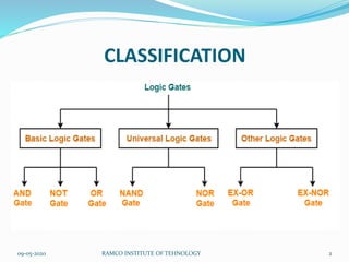
5. AND GATE
The output of AND gate is high (‘1’) if all of its inputs are
high (‘1’).
The output of AND gate is low (‘0’) if any one of its inputs
is low (‘0’).
09-05-2020 RAMCO INSTITUTE OF TEHNOLOGY 5
13. OR GATE
The output of OR gate is high (‘1’) if any one of its inputs is
high (‘1’).
The output of OR gate is low (‘0’) if all of its inputs are low
(‘0’).
09-05-2020 RAMCO INSTITUTE OF TEHNOLOGY 13
21. NOT GATE
The output of NOT gate is high (‘1’) if its input is low (‘0’).
The output of NOT gate is low (‘0’) if its input is high (‘1’).
It is clear that NOT gate simply inverts the given input.
Since NOT gate simply inverts the given input, therefore it
is also known as Inverter Gate.
09-05-2020 RAMCO INSTITUTE OF TEHNOLOGY 21
28. NAND GATE
A NAND Gate is constructed by connecting a NOT Gate at
the output terminal of the AND Gate.
The output of NAND gate is high (‘1’) if at least one of its
inputs is low (‘0’).
The output of NAND gate is low (‘0’) if all of its inputs are
high (‘1’).
09-05-2020 RAMCO INSTITUTE OF TEHNOLOGY 28
36. NOR GATE
A NOR Gate is constructed by connecting a NOT Gate at
the output terminal of the OR Gate.
The output of OR gate is high (‘1’) if all of its inputs are low
(‘0’).
The output of OR gate is low (‘0’) if any of its inputs is high
(‘1’).
09-05-2020 RAMCO INSTITUTE OF TEHNOLOGY 36
45. EXOR GATE
The logic gate which gives high output (i.e., 1) if either
input A or input B but not both are high (i.e. 1) is called
exclusive OR gate or the XOR gate.
It may be noted that if both the inputs of the XOR gate are
high, then the output is low (i.e., 0).
09-05-2020 RAMCO INSTITUTE OF TEHNOLOGY 45
47. TRUTH TABLE
A B Y =
A ⊕ B
0 0 0
0 1 1
1 0 1
1 1 0
A B C Y =
A ⊕ B ⊕ C
0 0 0 0
0 0 1 1
0 1 0 1
0 1 1 0
1 0 0 1
1 0 1 0
1 1 0 0
1 1 1 1
09-05-2020 RAMCO INSTITUTE OF TEHNOLOGY 47
52. EXNOR GATE
The logic function implemented by a 2-input Ex-NOR gate
is given as “when both A AND B are the SAME” will give an
output at Q.
In general, an Exclusive-NOR gate will give an output value
of logic “1” ONLY when there are an EVEN number of 1’s on
the inputs to the gate (the inverse of the Ex-OR gate)
except when all its inputs are “LOW”.
09-05-2020 RAMCO INSTITUTE OF TEHNOLOGY 52
59. LOGIC GATES and THEIR ICs
IC NUMBER NAME OF THE GATE
7400 NAND
7402 NOR
7404 NOT
7408 AND
7432 OR
7486 EXOR/ XOR/ EOR
74266 EXNOR/ XNOR/ ENOR
09-05-2020 RAMCO INSTITUTE OF TEHNOLOGY 59