SlideShare a Scribd company logo
1
NUMBER SYSTEMS &
BOOLEAN ALGEBRA
Presented By:
Veera Boopathy.E
Assistant Professor,
Department of ECE,
Karpagam Institute of Technology,
Coimbatore.
Overview
Number Systems - Arithmetic Operations -
Binary Codes- Boolean Algebra and Logic Gates -
Theorems and Properties of Boolean Algebra -
Boolean Functions - Canonical and Standard
Forms - Simplification of Boolean Functions
using Karnaugh Map - Logic Gates – NAND and
NOR Implementations. .
Karpagam Insitute of Technology 2
NUMBER SYSTEM
• Number system defines a set of values which are
used to represent a quantity.
• Radix or Base denotes total number of symbols
exists to represent a value.
NUMBER SYSTEM BASE or RADIX (r) NUMBERS : 0 to (r-1)
Binary 2 0, 1
Octal 8 0,1,2,3,4,5,6,7
Decimal 10 0,1,2,3,4,5,6,7,8,9
Duodecimal 12 0,1,2,3,4,5,6,7,8,9,A,B
Hexadecimal 16 0,1,2,3,4,5,6,7,8,9,A,B,C,D,E,F
NUMBER SYSTEM (cont.)
NUMBER SYSTEMS & CODES
WEIGHTED CODES (weights on
each position)
Decimal, Binary, Octal,
Hexadecimal, BCD codes…etc
NON-WEIGHTED CODES (weights
on each position
Grey Code, Excess-3 codes,..etc
NUMBER SYSTEM (cont.)
• Let
 r1 = base of 1st number system
 r2 = base of 2nd number system
 N1 = total number of digits in 1st number system used to represent
quantity
 N2 = total number of digits in 2nd number system used to represent
quantity
• Then
 r1<r2
 N1>N2
• EXAMPLE:
 (7392)10=(1110011100000)2
 (7392)10=(16340)8
 (7392)10=(1CE0)16
• Hence radix increases number of digits to represent quantity
decreases
BINARY NUMBER SYSTEM
(INTRODUCTION)
• Computer system operates using binary
number systems.
• r=2 => 0 to (r-1) => 0 and 1
• Each and every unit of binary number is called
Binary digit (BIT).
4 BIT= 1 nibble
8 BIT=1 byte
16 BIT=1 word
32 BIT=1 double word
DECIMAL TO BINARY CONVERSION
• RULE: To convert decimal to any other base ‘r’
then divide integer part by ‘r’ and multiply
fractional part by ‘r’.
• Example 1
• (13)10 = (?)2
2 13
2 6 - 1
2 3 - 0
2 1 - 1
0 - 1
LSB
MS
B
DECIMAL TO BINARY CONVERSION
• Example 2
• (25.625)10 = (?)2
2 25
2 12 - 1
2 6 - 0
2 3 - 0
2 1 - 1
0 - 1
LSB
MS
B
0.25 X 2 = 0.50
0.5 X 2 = 1.0
DECIMAL TO OCTAL CONVERSION
• To convert Decimal to Octal then divide
integer part by ‘8’ and multiply fractional part
by ‘8’.
• Example 1
• (112)10 = (?)8
8 112
8 14 - 0
8 1 - 6
0 - 1
LSB
MS
B
DECIMAL TO OCTAL CONVERSION
• Example 2
• (25.625)10 = (?)8
8 25
8 3 - 1
0 - 3
LSB
MS
B
• To convert Decimal to Hexadecimal then
divide integer part by ‘16’ and multiply
fractional part by ‘16’.
• Example 1
• (254)10 = (?)16
16 254
16 15 - 14
0 - 15
LSB
MS
B
DECIMAL TO HEXADECIMAL CONVERSION
E
F
DECIMAL TO HEXADECIMAL CONVERSION
• Example 2
• (25.625)10 = (?)16
16 25
16 1 - 9
0 - 1
LSB
MS
B
A
BINARY TO DECIMAL CONVERSION
• RULE (any number system to decimal):
(a3 a2 a1 a0 . a-1 a-2)r
= (?)10
={ (a3 x r3) + (a2 x r2) + (a1 x r1) + (a0 x r0) + (a-1 x r-1) + (a-2 x r-2) }
=( )10
r3 r2 r1 r0 r-1
r-2
BINARY TO DECIMAL CONVERSION
• Example
(10101.11)2 = (?)10
(10101.11)2
= (1 x 24) + (0 x 23) + (1 x 22) + (0 x 21) + (1 x 20) + (1 x 2-1) + (1 x 2-2)
= (1 x 16) + (0 x 8) + (1 x 4) + (0 x 2) + (1 x 1) + (1 /2) + (1/4)
= 16 + 0 + 4 + 0 + 1 + 0.5 + 0.25
= (21.75)10
24 23 22 21 20 2-1 2-2
OCTAL TO DECIMAL CONVERSION
• Example
(57.4)8 = (?)10
(57.4)8
= (5 x 81) + (7 x 80) + (4 x 8-1)
= (5 x 8) + (7 x 1) + (4 / 8)
= 40 + 7 + 0.5
= (47.5)10
81 80 8-1
HEXADECIMAL TO DECIMAL CONVERSION
• Example
(BAD)16 = (?)10
(BAD)16
= (B x 162) + (A x 161) + (D x 160)
= (11 x 256) + (10 x 16) + (13 x 1)
= 2816 + 160 + 13
= (2989)10
162 161 160
OCTAL NUMBER SYSTEM
• In octal number system eight different digits exists.
r=8 → 0 to (8-1) → 0 to 7 → 0,1,2,3,4,5,6,7
• Each of digit can be represented by 3-bit equivalent
number.
Octal
Binary value
421
0 000
1 001
2 010
3 011
4 100
5 101
6 110
7 111
OCTAL TO BINARY CONVERSION
• Example 1
(37.45)8=(?)2
(37.45)8 = (011111.100101)2
• Example 2
(26.07)8=(?)2
(26.07)8 = (010110.000111)2
011 111 . 100 101
010 110 . 000 111
Octal
Binary value
421
0 000
1 001
2 010
3 011
4 100
5 101
6 110
7 111
BINARY TO OCTAL CONVERSION
Step 1:
Mark the binary point
Step 2:
For integer part go from right to left and make group
of 3 bits
Step 3:
For fractional part go from left to right and make
group of 3 bits
BINARY TO OCTAL CONVERSION
• Example 1
(10110.11)2=(?)8
010110.110 = (26.6)8
Integer part Fractional part
6
2
6
• Example 2
(1001.1)2=(?)8
001001.100 = (11.4)8
Integer part Fractional part
1
1 4
HEXADECIMAL NUMBER SYSTEM
• In hexa-decimal number system 16 different digits exists.
r=16 → 0 to (16-1) → 0 to 15 → 0,1,2,3,4,5,6,7,8,9,A,B,C,D,E,F
• Each of digit can be represented by 3-bit equivalent number.
Hexadecimal
Binary value
8421
0 0000
1 0001
2 0010
3 0011
4 0100
5 0101
6 0110
7 0111
8 1000
9 1001
A 1010
B 1011
C 1100
D 1101
E 1110
F 1111
HEXADECIMAL TO BINARY CONVERSION
• Example 1
(25.9A)16=(?)2
(25.9A)16 = (00100101.10011010)2
• Example 2
(CAFE.3D)16=(?)2
(CAFE.3D)16 = (1100101011111110.00111101)2
0010 0101 . 1001
1010
1100 1010 1111 1110 . 0011 1101
Hexa
decim
al
Binary
value
8421
0 0000
1 0001
2 0010
3 0011
4 0100
5 0101
6 0110
7 0111
8 1000
9 1001
A 1010
B 1011
C 1100
D 1101
E 1110
F 1111
BINARY TO HEXADECIMAL CONVERSION
Step 1:
Mark the binary point
Step 2:
For integer part go from right to left and make group
of 4 bits
Step 3:
For fractional part go from left to right and make
group of 4 bits
BINARY TO HEXADECIMAL CONVERSION
• Example 1
(10110.11)2=(?)16
00010110.1100 =(16.C)16
Integer part Fractional part
6
1
C
Hexa
decimal
Binary
value
8421
0 0000
1 0001
2 0010
3 0011
4 0100
5 0101
6 0110
7 0111
8 1000
9 1001
A 1010
B 1011
C 1100
D 1101
E 1110
F 1111
HEXADECIMAL TO OCTAL CONVERSION
• Example 1:
(CAD)16 = (?)8
Step 1: Convert Hexadecimal to Binary
(CAD)16 = (110010101101)2
Step 2: Convert Binary to Octal
(110010101101)2 = (6255)8
HEXADECIMAL BINARY OCTAL
OCTAL TO HEXADECIMAL CONVERSION
• Example:
(652)8 = (?)16
Step 1: Convert Octal to Binary
(652)8 = (110101010)2
Step 2: Convert Binary to Hexadecimal
(110101010)2 = (1AA)16
OCTAL BINARY HEXADECIMAL
1’s COMPLEMENT OF BINARY NUMBER
• 1’s complement of binary number is obtained
by changing all 1s to 0s and all 0s to 1s.
• Example:
Find 1’s complement of (110101110)2
Binary Number 1 1 0 1 0 1 1 1 0
1’s complement 0 0 1 0 1 0 0 0 1
2’s COMPLEMENT OF BINARY NUMBER
• 2’s complement = 1’s complement + 1
• Example:
Find 1’s complement of (110101110)2
Binary Number 1 1 0 1 0 1 1 1 0
1’s complement 0 0 1 0 1 0 0 0 1
Boolean Algebra - Theorems and Properties of
Boolean Algebra
10/6/2022 Karpagam Insitute of Technology 29
BOOLEAN POSTULATES AND LAWS:
10/6/2022 Karpagam Insitute of Technology 30
T1 : Commutative Law
(a) A + B = B + A
(b) A B = B A
T2 : Associate Law
(a) (A + B) + C = A + (B + C)
(b) (A B) C = A (B C)
T3 : Distributive Law
(a) A (B + C) = A B + A C
(b) A + (B C) = (A + B) (A + C)
T4 : Identity Law
(a) A + A = A
(b) A A = A
Logic Circuits
• A collection of individual logic gates connect with each other and
produce a logic design known as a Logic Circuit
• The following are the types of logic circuits:
– Decision making
– Memory
– A gate has two or more binary inputs and single output.
Logic Circuits
Basic Logic Gates
• The following are the three basic gates:
– NOT
– AND
– OR
– Each logic gate performs a different logic function.
You can derive logical function or any Boolean or
logic expression by combining these three gates.
NOT Gate
• The simplest form of a digital logic circuit is the inverter or the NOT
gate
• It consists of one input and one output and the input can only be
binary numbers namely; 0 and 1
the truth table for NOT Gate:
33
OR Gate
• The OR gate is another basic logic gate
• Like the AND gate, it can have two or more inputs and a single output
• The operation of OR gate is such that the output is a binary 1 if any one or all
inputs are binary 1 and the output is binary 0 only when all the inputs are binary 0
34
AND Gate
• The AND gate is a logic circuit that has two or more inputs and a single output
• The operation of the gate is such that the output of the gate is a binary 1 if and
only if all inputs are binary 1
• Similarly, if any one or more inputs are binary 0, the output will be binary 0.
Fundamentals of Digital Electronics - Logic
Gates
35
NAND Gate
• The term NAND is a contraction of the expression NOT-AND gate
• A NAND gate, is an AND gate followed by an inverter
• The algebraic output expression of the NAND gate is Y = A.B
36
NOR Gate
• The term NOR is a contradiction of the expression NOT-OR
• A NOR gate, is an OR gate followed by an inverter
• The algebraic output expression of the NOR gate is Y = A + B
37
EX-OR and EX-NOR Gates
• EX-OR and EX-NOR are digital logic circuits
that may use two or more inputs
• EX-NOR gate returns the output opposite to
EX-OR gate
• EX-OR and EX-NOR gates are also denoted by
XOR and XNOR respectively.
38
EXOR Gate
• The Ex-OR (Exclusive- OR) gate returns high output with one of two high inputs (but not with both
high inputs or both low inputs)
• For example, if both the inputs are binary 0 or 1, it will return the output as 0. Similarly, if one input
is binary 1 and another is binary 0, the output will be 1 (high)
• The operation for the Ex-OR gate is denoted by encircled plus symbol
• The Ex-OR operation is widely used in digital circuits.
• The algebraic output expression of the Ex-OR gate is Y = A ⊕ B =
39
EXNOR Gate
• The Ex-NOR (Exclusive- NOR) gate is a circuit that returns low output with one of two high inputs
(but not with both high inputs)
• For example, if both the inputs are binary 0 or 1, it will return the output as 1. Similarly, if one input
is binary 1 and another is binary 0, the output will be 0 (low)
• The symbol for the Ex-NOR gate is denoted by encircled plus symbol which inverts the binary values
• The algebraic output expression of the Ex-NOR gate is Y =
40
Applications of Logic Gates
• The following are some of the applications of Logic
gates:
– Build complex systems that can be used to different fields
such as
• Genetic engineering,
• Nanotechnology,
• Industrial Fermentation,
• Metabolic engineering and
• Medicine
– Construct multiplexers, adders and multipliers.
– Perform several parallel logical operations
– Used for a simple house alarm or fire alarm or in the circuit
of automated machine manufacturing industry
41
Karnaugh Maps (K-Maps)
•A visual way to simplify logic
expressions
•It gives the most simplified form
of the expression
Rules to obtain the most simplified
expression
•Simplification of logic expression using Boolean algebra is awkward because:
–it lacks specific rules to predict the most suitable next step in the simplification
process
–it is difficult to determine whether the simplest form has been achieved.
•A Karnaugh map is a graphical method used to obtained the most simplified form of
an expression in a standard form (Sum-of-Products or Product-of-Sums).
•The simplest form of an expression is the one that has the minimum number of
terms with the least number of literals (variables) in each term.
•By simplifying an expression to the one that uses the minimum number of terms, we
ensure that the function will be implemented with the minimum number of gates.
•By simplifying an expression to the one that uses the least number of literals for
each terms, we ensure that the function will be implemented with gates that have
the minimum number of inputs.
Three-Variable K-Maps
 
 C
B
(0,4)
f  
 B
A
(4,5)
f  
 B
(0,1,4,5)
f  
 A
(0,1,2,3)
f
BC
00
0
01
1
11 10
A
1 0 0 0
1 0 0 0
BC
00
0
01
1
11 10
A
0 0 0 0
1 1 0 0
BC
00
0
01
1
11 10
A
1 1 1 1
0 0 0 0
BC
00
0
01
1
11 10
A
1 1 0 0
1 1 0 0
 
 C
A
(0,4)
f  
 C
A
(4,6)
f  
 C
A
(0,2)
f  
 C
(0,2,4,6)
f
BC
00
0
01
1
11 10
A
0 1 1 0
0 0 0 0
BC
00
0
01
1
11 10
A
0 0 0 0
1 0 0 1
BC
00
0
01
1
11 10
A
1 0 0 1
1 0 0 1
BC
00
0
01
1
11 10
A
1 0 0 1
0 0 0 0
Four-Variable K-Maps
 


 D
C
B
(0,8)
f  


 D
C
B
(5,13)
f  


 D
B
A
(13,15)
f  


 D
B
A
(4,6)
f
 

 C
A
(2,3,6,7)
f  

 D
B
)
(4,6,12,14
f  

 C
B
)
(2,3,10,11
f  

 D
B
(0,2,8,10)
f
CD
00
00
01
01
11
11
10
10
AB
1 0 0 0
0 0 0 0
0 0 0 0
1 0 0 0
CD
00
00
01
01
11
11
10
10
AB
0 0 0 0
0 1 0 0
0 1 0 0
0 0 0 0
CD
00
00
01
01
11
11
10
10
AB
0 0 0 0
0 0 0 0
0 1 1 0
0 0 0 0
CD
00
00
01
01
11
11
10
10
AB
0 0 0 0
1 0 0 1
0 0 0 0
0 0 0 0
CD
00
00
01
01
11
11
10
10
AB
0 0 1 1
0 0 1 1
0 0 0 0
0 0 0 0
CD
00
00
01
01
11
11
10
10
AB
0 0 0 0
1 0 0 1
1 0 0 1
0 0 0 0
CD
00
00
01
01
11
11
10
10
AB
0 0 1 1
0 0 0 0
0 0 0 0
0 0 1 1
CD
00
00
01
01
11
11
10
10
AB
1 0 0 1
0 0 0 0
0 0 0 0
1 0 0 1
Four-Variable K-Maps
CD
00
00
01
01
11
11
10
10
AB
0 0 0 0
1 1 1 1
0 0 0 0
0 0 0 0
CD
00
00
01
01
11
11
10
10
AB
0 0 1 0
0 0 1 0
0 0 1 0
0 0 1 0
CD
00
00
01
01
11
11
10
10
AB
1 0 1 0
0 1 0 1
1 0 1 0
0 1 0 1
CD
00
00
01
01
11
11
10
10
AB
0 1 0 1
1 0 1 0
0 1 0 1
1 0 1 0
CD
00
00
01
01
11
11
10
10
AB
0 1 1 0
0 1 1 0
0 1 1 0
0 1 1 0
CD
00
00
01
01
11
11
10
10
AB
1 0 0 1
1 0 0 1
1 0 0 1
1 0 0 1
CD
00
00
01
01
11
11
10
10
AB
0 0 0 0
1 1 1 1
1 1 1 1
0 0 0 0
CD
00
00
01
01
11
11
10
10
AB
1 1 1 1
0 0 0 0
0 0 0 0
1 1 1 1
f (4,5,6,7) A B
  
 f (3,7,11,15) C D
  

f (0,3,5,6,9,10,12,15)
  f (1,2,4,7,8,11,13,14)
 
f A B C D
    f A B C D
   
f (1,3,5,7,9,11,13,15)
  f (0,2,4,6,8,10,12,14)
  f (4,5,6,7,12,13,14,15)
  f (0,1,2,3,8,9,10,11)
 
f D
 f D
 f B
 f B

Quiz – Test your knowledge
• Q1. The binary number 10101 is
equivalent to decimal number …………..
1.19
2.12
3.27
4.21
• Answer : 4
10/6/2022 Karpagam Insitute of Technology 47
• Q2. The universal gate is ………………
1. NAND gate
2. OR gate
3. AND gate
4. None of the above
• Answer : 1
• Q3. The inverter is ……………
1. NOT gate
2. OR gate
3. AND gate
4. None of the above
• Answer : 1
• Q5. The NOR gate is OR gate followed by ………………
1. AND gate
2. NAND gate
3. NOT gate
4. None of the above
• Answer : 3
10/6/2022 Karpagam Insitute of Technology 48
ASSIGNMENT
• Simply boolean expression F = ABC + ABD + BCD using Karnaugh –Maps
and design them using NAND gates only.
• Simply boolean expression f = Π(1, 3, 5, 7, 13, 15) using Karnaugh –Maps
and design them using NOR gates only.
• Simply boolean expression f = m(2, 6, 9, 12) + d (0, 3) using Karnaugh –
Maps and design them using NAND gates only.
• Simply boolean expression f = m(6, 9, 11) + d (1, 5, 13) using Karnaugh –
Maps and design them using NOR gates only.
• Minimize the following function using a Karnaugh map of five variables:
F= m(2, 4, 6, 8, 10, 12, 14, 17, 19, 21, 23, 24, 25, 26, 27, 29, 31)
10/6/2022 Karpagam Insitute of Technology 49
Ad

More Related Content

What's hot (20)

Introduction to Counters
Introduction to CountersIntroduction to Counters
Introduction to Counters
ISMT College
 
Sequential circuits
Sequential circuitsSequential circuits
Sequential circuits
Paresh Parmar
 
adder and subtractor
 adder and subtractor adder and subtractor
adder and subtractor
Unsa Shakir
 
KARNAUGH MAP(K-MAP)
KARNAUGH MAP(K-MAP)KARNAUGH MAP(K-MAP)
KARNAUGH MAP(K-MAP)
mihir jain
 
13 Boolean Algebra
13 Boolean Algebra13 Boolean Algebra
13 Boolean Algebra
Praveen M Jigajinni
 
Digital logic design part1
Digital logic design part1Digital logic design part1
Digital logic design part1
Vaagdevi College of Engineering
 
full subtractor
full subtractorfull subtractor
full subtractor
Amodh Pandey
 
Digital Logic Design
Digital Logic Design Digital Logic Design
Digital Logic Design
Vaagdevi College of Engineering
 
Chapter 03 Boolean Algebra and Combinational Logic
Chapter 03 Boolean Algebra and Combinational LogicChapter 03 Boolean Algebra and Combinational Logic
Chapter 03 Boolean Algebra and Combinational Logic
SSE_AndyLi
 
Adder ppt
Adder pptAdder ppt
Adder ppt
Avinash Jadhav
 
boolean algrebra and logic gates in short
boolean algrebra and logic gates in shortboolean algrebra and logic gates in short
boolean algrebra and logic gates in short
Rojin Khadka
 
Adder substracter
Adder substracterAdder substracter
Adder substracter
WanNurdiana
 
Complements of numbers
Complements of numbersComplements of numbers
Complements of numbers
Kiriti Varkur
 
Boolean algebra & logic gates
Boolean algebra & logic gatesBoolean algebra & logic gates
Boolean algebra & logic gates
Prof. Dr. K. Adisesha
 
Sequential logic circuits flip-flop pt 1
Sequential logic circuits   flip-flop pt 1Sequential logic circuits   flip-flop pt 1
Sequential logic circuits flip-flop pt 1
Sarah Sue Calbio
 
4 bit uni shift reg
4 bit uni shift reg4 bit uni shift reg
4 bit uni shift reg
E ER Yash nagaria
 
Latches and flip flop
Latches and flip flopLatches and flip flop
Latches and flip flop
Shuaib Hotak
 
Multiplexers
MultiplexersMultiplexers
Multiplexers
Saloni Jain
 
Decoders-Digital Electronics
Decoders-Digital ElectronicsDecoders-Digital Electronics
Decoders-Digital Electronics
Paurav Shah
 
SHIFT REGISTERS
SHIFT REGISTERSSHIFT REGISTERS
SHIFT REGISTERS
kumari36
 

Similar to Number_Systems_and_Boolean_Algebra.ppt (20)

21EC201– Digital Principles and system design.pptx
21EC201– Digital Principles and system design.pptx21EC201– Digital Principles and system design.pptx
21EC201– Digital Principles and system design.pptx
GobinathAECEJRF1101
 
Dpsd lecture-notes
Dpsd lecture-notesDpsd lecture-notes
Dpsd lecture-notes
AVC College of Engineering
 
BEEE - Part B - Unit 3 PPT BEEE - Part B - Unit 3 PPT.ppt
BEEE - Part B - Unit 3 PPT BEEE - Part B - Unit 3 PPT.pptBEEE - Part B - Unit 3 PPT BEEE - Part B - Unit 3 PPT.ppt
BEEE - Part B - Unit 3 PPT BEEE - Part B - Unit 3 PPT.ppt
Drsivakumar12
 
Number System, nubmers and binary addition
Number System, nubmers and binary additionNumber System, nubmers and binary addition
Number System, nubmers and binary addition
ninjachavez
 
UNIT-1- Logic gates and Boolean algebras
UNIT-1- Logic gates and Boolean algebrasUNIT-1- Logic gates and Boolean algebras
UNIT-1- Logic gates and Boolean algebras
nithyainfo
 
UNIT-1_CSA.pdf
UNIT-1_CSA.pdfUNIT-1_CSA.pdf
UNIT-1_CSA.pdf
ShabbeerBasha8
 
Chapter 2 Boolean Algebra (part 2)
Chapter 2 Boolean Algebra (part 2)Chapter 2 Boolean Algebra (part 2)
Chapter 2 Boolean Algebra (part 2)
Frankie Jones
 
Chapter 1-1. Digital Systems, Number systems
Chapter 1-1. Digital Systems, Number systemsChapter 1-1. Digital Systems, Number systems
Chapter 1-1. Digital Systems, Number systems
sytan2004
 
Number Systems.ppt
Number Systems.pptNumber Systems.ppt
Number Systems.ppt
GnanaDeepikaMeduri
 
chapter 3 Boolean algebra (2).pptx
chapter 3 Boolean algebra (2).pptxchapter 3 Boolean algebra (2).pptx
chapter 3 Boolean algebra (2).pptx
RithinA1
 
dld 01-introduction
dld 01-introductiondld 01-introduction
dld 01-introduction
United International University
 
Digital Logic Design lec 2 slide.ppt DLD Lec 1.ppt
Digital Logic Design lec 2 slide.ppt DLD Lec 1.pptDigital Logic Design lec 2 slide.ppt DLD Lec 1.ppt
Digital Logic Design lec 2 slide.ppt DLD Lec 1.ppt
humairafatima22
 
Unit-1.pptx
Unit-1.pptxUnit-1.pptx
Unit-1.pptx
AshwiniMate10
 
02-gates-w.pptx
02-gates-w.pptx02-gates-w.pptx
02-gates-w.pptx
039JagadeeswaranS
 
Finite word length effects
Finite word length effectsFinite word length effects
Finite word length effects
PeriyanayagiS
 
Digital Electronics – Unit I.pdf
Digital Electronics – Unit I.pdfDigital Electronics – Unit I.pdf
Digital Electronics – Unit I.pdf
Kannan Kanagaraj
 
Digital Electronics Unit_1.pptx
Digital Electronics Unit_1.pptxDigital Electronics Unit_1.pptx
Digital Electronics Unit_1.pptx
Thapar Institute
 
Name dld preparation
Name dld preparationName dld preparation
Name dld preparation
Padam Rai
 
DLD-Introduction.pptx
DLD-Introduction.pptxDLD-Introduction.pptx
DLD-Introduction.pptx
UzairAhmadWalana
 
DE notes
DE notesDE notes
DE notes
Prof. Dr. K. Adisesha
 
21EC201– Digital Principles and system design.pptx
21EC201– Digital Principles and system design.pptx21EC201– Digital Principles and system design.pptx
21EC201– Digital Principles and system design.pptx
GobinathAECEJRF1101
 
BEEE - Part B - Unit 3 PPT BEEE - Part B - Unit 3 PPT.ppt
BEEE - Part B - Unit 3 PPT BEEE - Part B - Unit 3 PPT.pptBEEE - Part B - Unit 3 PPT BEEE - Part B - Unit 3 PPT.ppt
BEEE - Part B - Unit 3 PPT BEEE - Part B - Unit 3 PPT.ppt
Drsivakumar12
 
Number System, nubmers and binary addition
Number System, nubmers and binary additionNumber System, nubmers and binary addition
Number System, nubmers and binary addition
ninjachavez
 
UNIT-1- Logic gates and Boolean algebras
UNIT-1- Logic gates and Boolean algebrasUNIT-1- Logic gates and Boolean algebras
UNIT-1- Logic gates and Boolean algebras
nithyainfo
 
Chapter 2 Boolean Algebra (part 2)
Chapter 2 Boolean Algebra (part 2)Chapter 2 Boolean Algebra (part 2)
Chapter 2 Boolean Algebra (part 2)
Frankie Jones
 
Chapter 1-1. Digital Systems, Number systems
Chapter 1-1. Digital Systems, Number systemsChapter 1-1. Digital Systems, Number systems
Chapter 1-1. Digital Systems, Number systems
sytan2004
 
chapter 3 Boolean algebra (2).pptx
chapter 3 Boolean algebra (2).pptxchapter 3 Boolean algebra (2).pptx
chapter 3 Boolean algebra (2).pptx
RithinA1
 
Digital Logic Design lec 2 slide.ppt DLD Lec 1.ppt
Digital Logic Design lec 2 slide.ppt DLD Lec 1.pptDigital Logic Design lec 2 slide.ppt DLD Lec 1.ppt
Digital Logic Design lec 2 slide.ppt DLD Lec 1.ppt
humairafatima22
 
Finite word length effects
Finite word length effectsFinite word length effects
Finite word length effects
PeriyanayagiS
 
Digital Electronics – Unit I.pdf
Digital Electronics – Unit I.pdfDigital Electronics – Unit I.pdf
Digital Electronics – Unit I.pdf
Kannan Kanagaraj
 
Digital Electronics Unit_1.pptx
Digital Electronics Unit_1.pptxDigital Electronics Unit_1.pptx
Digital Electronics Unit_1.pptx
Thapar Institute
 
Name dld preparation
Name dld preparationName dld preparation
Name dld preparation
Padam Rai
 
Ad

Recently uploaded (20)

Smart Storage Solutions.pptx for production engineering
Smart Storage Solutions.pptx for production engineeringSmart Storage Solutions.pptx for production engineering
Smart Storage Solutions.pptx for production engineering
rushikeshnavghare94
 
Level 1-Safety.pptx Presentation of Electrical Safety
Level 1-Safety.pptx Presentation of Electrical SafetyLevel 1-Safety.pptx Presentation of Electrical Safety
Level 1-Safety.pptx Presentation of Electrical Safety
JoseAlbertoCariasDel
 
Oil-gas_Unconventional oil and gass_reseviours.pdf
Oil-gas_Unconventional oil and gass_reseviours.pdfOil-gas_Unconventional oil and gass_reseviours.pdf
Oil-gas_Unconventional oil and gass_reseviours.pdf
M7md3li2
 
Machine learning project on employee attrition detection using (2).pptx
Machine learning project on employee attrition detection using (2).pptxMachine learning project on employee attrition detection using (2).pptx
Machine learning project on employee attrition detection using (2).pptx
rajeswari89780
 
MAQUINARIA MINAS CEMA 6th Edition (1).pdf
MAQUINARIA MINAS CEMA 6th Edition (1).pdfMAQUINARIA MINAS CEMA 6th Edition (1).pdf
MAQUINARIA MINAS CEMA 6th Edition (1).pdf
ssuser562df4
 
DT REPORT by Tech titan GROUP to introduce the subject design Thinking
DT REPORT by Tech titan GROUP to introduce the subject design ThinkingDT REPORT by Tech titan GROUP to introduce the subject design Thinking
DT REPORT by Tech titan GROUP to introduce the subject design Thinking
DhruvChotaliya2
 
211421893-M-Tech-CIVIL-Structural-Engineering-pdf.pdf
211421893-M-Tech-CIVIL-Structural-Engineering-pdf.pdf211421893-M-Tech-CIVIL-Structural-Engineering-pdf.pdf
211421893-M-Tech-CIVIL-Structural-Engineering-pdf.pdf
inmishra17121973
 
Fort night presentation new0903 pdf.pdf.
Fort night presentation new0903 pdf.pdf.Fort night presentation new0903 pdf.pdf.
Fort night presentation new0903 pdf.pdf.
anuragmk56
 
The Gaussian Process Modeling Module in UQLab
The Gaussian Process Modeling Module in UQLabThe Gaussian Process Modeling Module in UQLab
The Gaussian Process Modeling Module in UQLab
Journal of Soft Computing in Civil Engineering
 
Artificial Intelligence (AI) basics.pptx
Artificial Intelligence (AI) basics.pptxArtificial Intelligence (AI) basics.pptx
Artificial Intelligence (AI) basics.pptx
aditichinar
 
Introduction to FLUID MECHANICS & KINEMATICS
Introduction to FLUID MECHANICS &  KINEMATICSIntroduction to FLUID MECHANICS &  KINEMATICS
Introduction to FLUID MECHANICS & KINEMATICS
narayanaswamygdas
 
Smart_Storage_Systems_Production_Engineering.pptx
Smart_Storage_Systems_Production_Engineering.pptxSmart_Storage_Systems_Production_Engineering.pptx
Smart_Storage_Systems_Production_Engineering.pptx
rushikeshnavghare94
 
"Boiler Feed Pump (BFP): Working, Applications, Advantages, and Limitations E...
"Boiler Feed Pump (BFP): Working, Applications, Advantages, and Limitations E..."Boiler Feed Pump (BFP): Working, Applications, Advantages, and Limitations E...
"Boiler Feed Pump (BFP): Working, Applications, Advantages, and Limitations E...
Infopitaara
 
Avnet Silica's PCIM 2025 Highlights Flyer
Avnet Silica's PCIM 2025 Highlights FlyerAvnet Silica's PCIM 2025 Highlights Flyer
Avnet Silica's PCIM 2025 Highlights Flyer
WillDavies22
 
Process Parameter Optimization for Minimizing Springback in Cold Drawing Proc...
Process Parameter Optimization for Minimizing Springback in Cold Drawing Proc...Process Parameter Optimization for Minimizing Springback in Cold Drawing Proc...
Process Parameter Optimization for Minimizing Springback in Cold Drawing Proc...
Journal of Soft Computing in Civil Engineering
 
Introduction to Zoomlion Earthmoving.pptx
Introduction to Zoomlion Earthmoving.pptxIntroduction to Zoomlion Earthmoving.pptx
Introduction to Zoomlion Earthmoving.pptx
AS1920
 
railway wheels, descaling after reheating and before forging
railway wheels, descaling after reheating and before forgingrailway wheels, descaling after reheating and before forging
railway wheels, descaling after reheating and before forging
Javad Kadkhodapour
 
Metal alkyne complexes.pptx in chemistry
Metal alkyne complexes.pptx in chemistryMetal alkyne complexes.pptx in chemistry
Metal alkyne complexes.pptx in chemistry
mee23nu
 
ELectronics Boards & Product Testing_Shiju.pdf
ELectronics Boards & Product Testing_Shiju.pdfELectronics Boards & Product Testing_Shiju.pdf
ELectronics Boards & Product Testing_Shiju.pdf
Shiju Jacob
 
Data Structures_Introduction to algorithms.pptx
Data Structures_Introduction to algorithms.pptxData Structures_Introduction to algorithms.pptx
Data Structures_Introduction to algorithms.pptx
RushaliDeshmukh2
 
Smart Storage Solutions.pptx for production engineering
Smart Storage Solutions.pptx for production engineeringSmart Storage Solutions.pptx for production engineering
Smart Storage Solutions.pptx for production engineering
rushikeshnavghare94
 
Level 1-Safety.pptx Presentation of Electrical Safety
Level 1-Safety.pptx Presentation of Electrical SafetyLevel 1-Safety.pptx Presentation of Electrical Safety
Level 1-Safety.pptx Presentation of Electrical Safety
JoseAlbertoCariasDel
 
Oil-gas_Unconventional oil and gass_reseviours.pdf
Oil-gas_Unconventional oil and gass_reseviours.pdfOil-gas_Unconventional oil and gass_reseviours.pdf
Oil-gas_Unconventional oil and gass_reseviours.pdf
M7md3li2
 
Machine learning project on employee attrition detection using (2).pptx
Machine learning project on employee attrition detection using (2).pptxMachine learning project on employee attrition detection using (2).pptx
Machine learning project on employee attrition detection using (2).pptx
rajeswari89780
 
MAQUINARIA MINAS CEMA 6th Edition (1).pdf
MAQUINARIA MINAS CEMA 6th Edition (1).pdfMAQUINARIA MINAS CEMA 6th Edition (1).pdf
MAQUINARIA MINAS CEMA 6th Edition (1).pdf
ssuser562df4
 
DT REPORT by Tech titan GROUP to introduce the subject design Thinking
DT REPORT by Tech titan GROUP to introduce the subject design ThinkingDT REPORT by Tech titan GROUP to introduce the subject design Thinking
DT REPORT by Tech titan GROUP to introduce the subject design Thinking
DhruvChotaliya2
 
211421893-M-Tech-CIVIL-Structural-Engineering-pdf.pdf
211421893-M-Tech-CIVIL-Structural-Engineering-pdf.pdf211421893-M-Tech-CIVIL-Structural-Engineering-pdf.pdf
211421893-M-Tech-CIVIL-Structural-Engineering-pdf.pdf
inmishra17121973
 
Fort night presentation new0903 pdf.pdf.
Fort night presentation new0903 pdf.pdf.Fort night presentation new0903 pdf.pdf.
Fort night presentation new0903 pdf.pdf.
anuragmk56
 
Artificial Intelligence (AI) basics.pptx
Artificial Intelligence (AI) basics.pptxArtificial Intelligence (AI) basics.pptx
Artificial Intelligence (AI) basics.pptx
aditichinar
 
Introduction to FLUID MECHANICS & KINEMATICS
Introduction to FLUID MECHANICS &  KINEMATICSIntroduction to FLUID MECHANICS &  KINEMATICS
Introduction to FLUID MECHANICS & KINEMATICS
narayanaswamygdas
 
Smart_Storage_Systems_Production_Engineering.pptx
Smart_Storage_Systems_Production_Engineering.pptxSmart_Storage_Systems_Production_Engineering.pptx
Smart_Storage_Systems_Production_Engineering.pptx
rushikeshnavghare94
 
"Boiler Feed Pump (BFP): Working, Applications, Advantages, and Limitations E...
"Boiler Feed Pump (BFP): Working, Applications, Advantages, and Limitations E..."Boiler Feed Pump (BFP): Working, Applications, Advantages, and Limitations E...
"Boiler Feed Pump (BFP): Working, Applications, Advantages, and Limitations E...
Infopitaara
 
Avnet Silica's PCIM 2025 Highlights Flyer
Avnet Silica's PCIM 2025 Highlights FlyerAvnet Silica's PCIM 2025 Highlights Flyer
Avnet Silica's PCIM 2025 Highlights Flyer
WillDavies22
 
Introduction to Zoomlion Earthmoving.pptx
Introduction to Zoomlion Earthmoving.pptxIntroduction to Zoomlion Earthmoving.pptx
Introduction to Zoomlion Earthmoving.pptx
AS1920
 
railway wheels, descaling after reheating and before forging
railway wheels, descaling after reheating and before forgingrailway wheels, descaling after reheating and before forging
railway wheels, descaling after reheating and before forging
Javad Kadkhodapour
 
Metal alkyne complexes.pptx in chemistry
Metal alkyne complexes.pptx in chemistryMetal alkyne complexes.pptx in chemistry
Metal alkyne complexes.pptx in chemistry
mee23nu
 
ELectronics Boards & Product Testing_Shiju.pdf
ELectronics Boards & Product Testing_Shiju.pdfELectronics Boards & Product Testing_Shiju.pdf
ELectronics Boards & Product Testing_Shiju.pdf
Shiju Jacob
 
Data Structures_Introduction to algorithms.pptx
Data Structures_Introduction to algorithms.pptxData Structures_Introduction to algorithms.pptx
Data Structures_Introduction to algorithms.pptx
RushaliDeshmukh2
 
Ad

Number_Systems_and_Boolean_Algebra.ppt

  • 1. 1 NUMBER SYSTEMS & BOOLEAN ALGEBRA Presented By: Veera Boopathy.E Assistant Professor, Department of ECE, Karpagam Institute of Technology, Coimbatore.
  • 2. Overview Number Systems - Arithmetic Operations - Binary Codes- Boolean Algebra and Logic Gates - Theorems and Properties of Boolean Algebra - Boolean Functions - Canonical and Standard Forms - Simplification of Boolean Functions using Karnaugh Map - Logic Gates – NAND and NOR Implementations. . Karpagam Insitute of Technology 2
  • 3. NUMBER SYSTEM • Number system defines a set of values which are used to represent a quantity. • Radix or Base denotes total number of symbols exists to represent a value. NUMBER SYSTEM BASE or RADIX (r) NUMBERS : 0 to (r-1) Binary 2 0, 1 Octal 8 0,1,2,3,4,5,6,7 Decimal 10 0,1,2,3,4,5,6,7,8,9 Duodecimal 12 0,1,2,3,4,5,6,7,8,9,A,B Hexadecimal 16 0,1,2,3,4,5,6,7,8,9,A,B,C,D,E,F
  • 4. NUMBER SYSTEM (cont.) NUMBER SYSTEMS & CODES WEIGHTED CODES (weights on each position) Decimal, Binary, Octal, Hexadecimal, BCD codes…etc NON-WEIGHTED CODES (weights on each position Grey Code, Excess-3 codes,..etc
  • 5. NUMBER SYSTEM (cont.) • Let  r1 = base of 1st number system  r2 = base of 2nd number system  N1 = total number of digits in 1st number system used to represent quantity  N2 = total number of digits in 2nd number system used to represent quantity • Then  r1<r2  N1>N2 • EXAMPLE:  (7392)10=(1110011100000)2  (7392)10=(16340)8  (7392)10=(1CE0)16 • Hence radix increases number of digits to represent quantity decreases
  • 6. BINARY NUMBER SYSTEM (INTRODUCTION) • Computer system operates using binary number systems. • r=2 => 0 to (r-1) => 0 and 1 • Each and every unit of binary number is called Binary digit (BIT). 4 BIT= 1 nibble 8 BIT=1 byte 16 BIT=1 word 32 BIT=1 double word
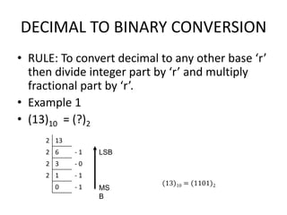
  • 7. DECIMAL TO BINARY CONVERSION • RULE: To convert decimal to any other base ‘r’ then divide integer part by ‘r’ and multiply fractional part by ‘r’. • Example 1 • (13)10 = (?)2 2 13 2 6 - 1 2 3 - 0 2 1 - 1 0 - 1 LSB MS B
  • 8. DECIMAL TO BINARY CONVERSION • Example 2 • (25.625)10 = (?)2 2 25 2 12 - 1 2 6 - 0 2 3 - 0 2 1 - 1 0 - 1 LSB MS B 0.25 X 2 = 0.50 0.5 X 2 = 1.0
  • 9. DECIMAL TO OCTAL CONVERSION • To convert Decimal to Octal then divide integer part by ‘8’ and multiply fractional part by ‘8’. • Example 1 • (112)10 = (?)8 8 112 8 14 - 0 8 1 - 6 0 - 1 LSB MS B
  • 10. DECIMAL TO OCTAL CONVERSION • Example 2 • (25.625)10 = (?)8 8 25 8 3 - 1 0 - 3 LSB MS B
  • 11. • To convert Decimal to Hexadecimal then divide integer part by ‘16’ and multiply fractional part by ‘16’. • Example 1 • (254)10 = (?)16 16 254 16 15 - 14 0 - 15 LSB MS B DECIMAL TO HEXADECIMAL CONVERSION E F
  • 12. DECIMAL TO HEXADECIMAL CONVERSION • Example 2 • (25.625)10 = (?)16 16 25 16 1 - 9 0 - 1 LSB MS B A
  • 13. BINARY TO DECIMAL CONVERSION • RULE (any number system to decimal): (a3 a2 a1 a0 . a-1 a-2)r = (?)10 ={ (a3 x r3) + (a2 x r2) + (a1 x r1) + (a0 x r0) + (a-1 x r-1) + (a-2 x r-2) } =( )10 r3 r2 r1 r0 r-1 r-2
  • 14. BINARY TO DECIMAL CONVERSION • Example (10101.11)2 = (?)10 (10101.11)2 = (1 x 24) + (0 x 23) + (1 x 22) + (0 x 21) + (1 x 20) + (1 x 2-1) + (1 x 2-2) = (1 x 16) + (0 x 8) + (1 x 4) + (0 x 2) + (1 x 1) + (1 /2) + (1/4) = 16 + 0 + 4 + 0 + 1 + 0.5 + 0.25 = (21.75)10 24 23 22 21 20 2-1 2-2
  • 15. OCTAL TO DECIMAL CONVERSION • Example (57.4)8 = (?)10 (57.4)8 = (5 x 81) + (7 x 80) + (4 x 8-1) = (5 x 8) + (7 x 1) + (4 / 8) = 40 + 7 + 0.5 = (47.5)10 81 80 8-1
  • 16. HEXADECIMAL TO DECIMAL CONVERSION • Example (BAD)16 = (?)10 (BAD)16 = (B x 162) + (A x 161) + (D x 160) = (11 x 256) + (10 x 16) + (13 x 1) = 2816 + 160 + 13 = (2989)10 162 161 160
  • 17. OCTAL NUMBER SYSTEM • In octal number system eight different digits exists. r=8 → 0 to (8-1) → 0 to 7 → 0,1,2,3,4,5,6,7 • Each of digit can be represented by 3-bit equivalent number. Octal Binary value 421 0 000 1 001 2 010 3 011 4 100 5 101 6 110 7 111
  • 18. OCTAL TO BINARY CONVERSION • Example 1 (37.45)8=(?)2 (37.45)8 = (011111.100101)2 • Example 2 (26.07)8=(?)2 (26.07)8 = (010110.000111)2 011 111 . 100 101 010 110 . 000 111 Octal Binary value 421 0 000 1 001 2 010 3 011 4 100 5 101 6 110 7 111
  • 19. BINARY TO OCTAL CONVERSION Step 1: Mark the binary point Step 2: For integer part go from right to left and make group of 3 bits Step 3: For fractional part go from left to right and make group of 3 bits
  • 20. BINARY TO OCTAL CONVERSION • Example 1 (10110.11)2=(?)8 010110.110 = (26.6)8 Integer part Fractional part 6 2 6 • Example 2 (1001.1)2=(?)8 001001.100 = (11.4)8 Integer part Fractional part 1 1 4
  • 21. HEXADECIMAL NUMBER SYSTEM • In hexa-decimal number system 16 different digits exists. r=16 → 0 to (16-1) → 0 to 15 → 0,1,2,3,4,5,6,7,8,9,A,B,C,D,E,F • Each of digit can be represented by 3-bit equivalent number. Hexadecimal Binary value 8421 0 0000 1 0001 2 0010 3 0011 4 0100 5 0101 6 0110 7 0111 8 1000 9 1001 A 1010 B 1011 C 1100 D 1101 E 1110 F 1111
  • 22. HEXADECIMAL TO BINARY CONVERSION • Example 1 (25.9A)16=(?)2 (25.9A)16 = (00100101.10011010)2 • Example 2 (CAFE.3D)16=(?)2 (CAFE.3D)16 = (1100101011111110.00111101)2 0010 0101 . 1001 1010 1100 1010 1111 1110 . 0011 1101 Hexa decim al Binary value 8421 0 0000 1 0001 2 0010 3 0011 4 0100 5 0101 6 0110 7 0111 8 1000 9 1001 A 1010 B 1011 C 1100 D 1101 E 1110 F 1111
  • 23. BINARY TO HEXADECIMAL CONVERSION Step 1: Mark the binary point Step 2: For integer part go from right to left and make group of 4 bits Step 3: For fractional part go from left to right and make group of 4 bits
  • 24. BINARY TO HEXADECIMAL CONVERSION • Example 1 (10110.11)2=(?)16 00010110.1100 =(16.C)16 Integer part Fractional part 6 1 C Hexa decimal Binary value 8421 0 0000 1 0001 2 0010 3 0011 4 0100 5 0101 6 0110 7 0111 8 1000 9 1001 A 1010 B 1011 C 1100 D 1101 E 1110 F 1111
  • 25. HEXADECIMAL TO OCTAL CONVERSION • Example 1: (CAD)16 = (?)8 Step 1: Convert Hexadecimal to Binary (CAD)16 = (110010101101)2 Step 2: Convert Binary to Octal (110010101101)2 = (6255)8 HEXADECIMAL BINARY OCTAL
  • 26. OCTAL TO HEXADECIMAL CONVERSION • Example: (652)8 = (?)16 Step 1: Convert Octal to Binary (652)8 = (110101010)2 Step 2: Convert Binary to Hexadecimal (110101010)2 = (1AA)16 OCTAL BINARY HEXADECIMAL
  • 27. 1’s COMPLEMENT OF BINARY NUMBER • 1’s complement of binary number is obtained by changing all 1s to 0s and all 0s to 1s. • Example: Find 1’s complement of (110101110)2 Binary Number 1 1 0 1 0 1 1 1 0 1’s complement 0 0 1 0 1 0 0 0 1
  • 28. 2’s COMPLEMENT OF BINARY NUMBER • 2’s complement = 1’s complement + 1 • Example: Find 1’s complement of (110101110)2 Binary Number 1 1 0 1 0 1 1 1 0 1’s complement 0 0 1 0 1 0 0 0 1
  • 29. Boolean Algebra - Theorems and Properties of Boolean Algebra 10/6/2022 Karpagam Insitute of Technology 29
  • 30. BOOLEAN POSTULATES AND LAWS: 10/6/2022 Karpagam Insitute of Technology 30 T1 : Commutative Law (a) A + B = B + A (b) A B = B A T2 : Associate Law (a) (A + B) + C = A + (B + C) (b) (A B) C = A (B C) T3 : Distributive Law (a) A (B + C) = A B + A C (b) A + (B C) = (A + B) (A + C) T4 : Identity Law (a) A + A = A (b) A A = A
  • 31. Logic Circuits • A collection of individual logic gates connect with each other and produce a logic design known as a Logic Circuit • The following are the types of logic circuits: – Decision making – Memory – A gate has two or more binary inputs and single output. Logic Circuits
  • 32. Basic Logic Gates • The following are the three basic gates: – NOT – AND – OR – Each logic gate performs a different logic function. You can derive logical function or any Boolean or logic expression by combining these three gates.
  • 33. NOT Gate • The simplest form of a digital logic circuit is the inverter or the NOT gate • It consists of one input and one output and the input can only be binary numbers namely; 0 and 1 the truth table for NOT Gate: 33
  • 34. OR Gate • The OR gate is another basic logic gate • Like the AND gate, it can have two or more inputs and a single output • The operation of OR gate is such that the output is a binary 1 if any one or all inputs are binary 1 and the output is binary 0 only when all the inputs are binary 0 34
  • 35. AND Gate • The AND gate is a logic circuit that has two or more inputs and a single output • The operation of the gate is such that the output of the gate is a binary 1 if and only if all inputs are binary 1 • Similarly, if any one or more inputs are binary 0, the output will be binary 0. Fundamentals of Digital Electronics - Logic Gates 35
  • 36. NAND Gate • The term NAND is a contraction of the expression NOT-AND gate • A NAND gate, is an AND gate followed by an inverter • The algebraic output expression of the NAND gate is Y = A.B 36
  • 37. NOR Gate • The term NOR is a contradiction of the expression NOT-OR • A NOR gate, is an OR gate followed by an inverter • The algebraic output expression of the NOR gate is Y = A + B 37
  • 38. EX-OR and EX-NOR Gates • EX-OR and EX-NOR are digital logic circuits that may use two or more inputs • EX-NOR gate returns the output opposite to EX-OR gate • EX-OR and EX-NOR gates are also denoted by XOR and XNOR respectively. 38
  • 39. EXOR Gate • The Ex-OR (Exclusive- OR) gate returns high output with one of two high inputs (but not with both high inputs or both low inputs) • For example, if both the inputs are binary 0 or 1, it will return the output as 0. Similarly, if one input is binary 1 and another is binary 0, the output will be 1 (high) • The operation for the Ex-OR gate is denoted by encircled plus symbol • The Ex-OR operation is widely used in digital circuits. • The algebraic output expression of the Ex-OR gate is Y = A ⊕ B = 39
  • 40. EXNOR Gate • The Ex-NOR (Exclusive- NOR) gate is a circuit that returns low output with one of two high inputs (but not with both high inputs) • For example, if both the inputs are binary 0 or 1, it will return the output as 1. Similarly, if one input is binary 1 and another is binary 0, the output will be 0 (low) • The symbol for the Ex-NOR gate is denoted by encircled plus symbol which inverts the binary values • The algebraic output expression of the Ex-NOR gate is Y = 40
  • 41. Applications of Logic Gates • The following are some of the applications of Logic gates: – Build complex systems that can be used to different fields such as • Genetic engineering, • Nanotechnology, • Industrial Fermentation, • Metabolic engineering and • Medicine – Construct multiplexers, adders and multipliers. – Perform several parallel logical operations – Used for a simple house alarm or fire alarm or in the circuit of automated machine manufacturing industry 41
  • 42. Karnaugh Maps (K-Maps) •A visual way to simplify logic expressions •It gives the most simplified form of the expression
  • 43. Rules to obtain the most simplified expression •Simplification of logic expression using Boolean algebra is awkward because: –it lacks specific rules to predict the most suitable next step in the simplification process –it is difficult to determine whether the simplest form has been achieved. •A Karnaugh map is a graphical method used to obtained the most simplified form of an expression in a standard form (Sum-of-Products or Product-of-Sums). •The simplest form of an expression is the one that has the minimum number of terms with the least number of literals (variables) in each term. •By simplifying an expression to the one that uses the minimum number of terms, we ensure that the function will be implemented with the minimum number of gates. •By simplifying an expression to the one that uses the least number of literals for each terms, we ensure that the function will be implemented with gates that have the minimum number of inputs.
  • 44. Three-Variable K-Maps    C B (0,4) f    B A (4,5) f    B (0,1,4,5) f    A (0,1,2,3) f BC 00 0 01 1 11 10 A 1 0 0 0 1 0 0 0 BC 00 0 01 1 11 10 A 0 0 0 0 1 1 0 0 BC 00 0 01 1 11 10 A 1 1 1 1 0 0 0 0 BC 00 0 01 1 11 10 A 1 1 0 0 1 1 0 0    C A (0,4) f    C A (4,6) f    C A (0,2) f    C (0,2,4,6) f BC 00 0 01 1 11 10 A 0 1 1 0 0 0 0 0 BC 00 0 01 1 11 10 A 0 0 0 0 1 0 0 1 BC 00 0 01 1 11 10 A 1 0 0 1 1 0 0 1 BC 00 0 01 1 11 10 A 1 0 0 1 0 0 0 0
  • 45. Four-Variable K-Maps      D C B (0,8) f      D C B (5,13) f      D B A (13,15) f      D B A (4,6) f     C A (2,3,6,7) f     D B ) (4,6,12,14 f     C B ) (2,3,10,11 f     D B (0,2,8,10) f CD 00 00 01 01 11 11 10 10 AB 1 0 0 0 0 0 0 0 0 0 0 0 1 0 0 0 CD 00 00 01 01 11 11 10 10 AB 0 0 0 0 0 1 0 0 0 1 0 0 0 0 0 0 CD 00 00 01 01 11 11 10 10 AB 0 0 0 0 0 0 0 0 0 1 1 0 0 0 0 0 CD 00 00 01 01 11 11 10 10 AB 0 0 0 0 1 0 0 1 0 0 0 0 0 0 0 0 CD 00 00 01 01 11 11 10 10 AB 0 0 1 1 0 0 1 1 0 0 0 0 0 0 0 0 CD 00 00 01 01 11 11 10 10 AB 0 0 0 0 1 0 0 1 1 0 0 1 0 0 0 0 CD 00 00 01 01 11 11 10 10 AB 0 0 1 1 0 0 0 0 0 0 0 0 0 0 1 1 CD 00 00 01 01 11 11 10 10 AB 1 0 0 1 0 0 0 0 0 0 0 0 1 0 0 1
  • 46. Four-Variable K-Maps CD 00 00 01 01 11 11 10 10 AB 0 0 0 0 1 1 1 1 0 0 0 0 0 0 0 0 CD 00 00 01 01 11 11 10 10 AB 0 0 1 0 0 0 1 0 0 0 1 0 0 0 1 0 CD 00 00 01 01 11 11 10 10 AB 1 0 1 0 0 1 0 1 1 0 1 0 0 1 0 1 CD 00 00 01 01 11 11 10 10 AB 0 1 0 1 1 0 1 0 0 1 0 1 1 0 1 0 CD 00 00 01 01 11 11 10 10 AB 0 1 1 0 0 1 1 0 0 1 1 0 0 1 1 0 CD 00 00 01 01 11 11 10 10 AB 1 0 0 1 1 0 0 1 1 0 0 1 1 0 0 1 CD 00 00 01 01 11 11 10 10 AB 0 0 0 0 1 1 1 1 1 1 1 1 0 0 0 0 CD 00 00 01 01 11 11 10 10 AB 1 1 1 1 0 0 0 0 0 0 0 0 1 1 1 1 f (4,5,6,7) A B     f (3,7,11,15) C D     f (0,3,5,6,9,10,12,15)   f (1,2,4,7,8,11,13,14)   f A B C D     f A B C D     f (1,3,5,7,9,11,13,15)   f (0,2,4,6,8,10,12,14)   f (4,5,6,7,12,13,14,15)   f (0,1,2,3,8,9,10,11)   f D  f D  f B  f B 
  • 47. Quiz – Test your knowledge • Q1. The binary number 10101 is equivalent to decimal number ………….. 1.19 2.12 3.27 4.21 • Answer : 4 10/6/2022 Karpagam Insitute of Technology 47
  • 48. • Q2. The universal gate is ……………… 1. NAND gate 2. OR gate 3. AND gate 4. None of the above • Answer : 1 • Q3. The inverter is …………… 1. NOT gate 2. OR gate 3. AND gate 4. None of the above • Answer : 1 • Q5. The NOR gate is OR gate followed by ……………… 1. AND gate 2. NAND gate 3. NOT gate 4. None of the above • Answer : 3 10/6/2022 Karpagam Insitute of Technology 48
  • 49. ASSIGNMENT • Simply boolean expression F = ABC + ABD + BCD using Karnaugh –Maps and design them using NAND gates only. • Simply boolean expression f = Π(1, 3, 5, 7, 13, 15) using Karnaugh –Maps and design them using NOR gates only. • Simply boolean expression f = m(2, 6, 9, 12) + d (0, 3) using Karnaugh – Maps and design them using NAND gates only. • Simply boolean expression f = m(6, 9, 11) + d (1, 5, 13) using Karnaugh – Maps and design them using NOR gates only. • Minimize the following function using a Karnaugh map of five variables: F= m(2, 4, 6, 8, 10, 12, 14, 17, 19, 21, 23, 24, 25, 26, 27, 29, 31) 10/6/2022 Karpagam Insitute of Technology 49