Programmable logic devices
Download as PPTX, PDF•0 likes•3,360 views

This document discusses programmable logic devices (PLDs), including their basic components and types. PLDs are integrated circuits that can be configured by the user to perform different logic functions. They contain programmable AND and OR gates that allow the user to define the logic function by programming the connections between the gates. Common types of PLDs include PROM, PAL, and PLA, which differ in whether their AND gates and/or OR gates are programmable. The document provides examples and diagrams to illustrate how basic logic functions can be implemented using each type of PLD.


Programmable logic devices
- 2. Programmable Logic Device (PLD) • A logic device is an electronic component which performs a definite function which is decided at the time of manufacture and will never change. • For example, a not gate always inverts the logic level of the input signal and does/can-do-nothing else. • On the other hand, Programmable Logic Devices (PLDs) are the components which do not have a specific function associated with them. • These can be configured to perform a certain function by the user, on a need basis and can further be changed to perform some other function at the later point of time, i.e. these are re-configurable. However, the amount of flexibility offered depends on their type.
- 3. • Programmable Logic Devices (PLDs) are the integrated circuits which contain an array of AND gates & another array of OR gates. • The process of entering the information into these devices is known as programming. • Here, the term programming refers to hardware programming but not software programming. • The internal logic gates AND/OR connections of PLDs can be changed/configured by a programming process
- 4. • One of the simplest programming technologies is to use fuses. • In the original state of the device, all the fuses are intact. • Programming the device involves blowing those fuses along the paths that must be removed in order to obtain the particular configuration of the desired logic function.
- 5. Array logic • A typical programmable logic device may have hundreds to millions of gates interconnected through hundreds to thousands of internal paths. • In order to show the internal logic diagram in a concise form, it is necessary to employ a special gate symbology applicable to array logic.
- 7. Types • Programmable Read Only Memory (PROM) • Programmable Array Logic (PAL) • Programmable Logic Array (PLA) • Assignment : Advantages of using PLDs:
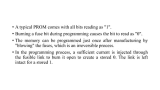
- 8. Programmable Read Only Memory (PROM) • Programmable ROM is a one-time programmable chip that, once programmed, cannot be erased or altered. • PROM is also referred as One Time Programmable(OTP) • These memories are bought in blank form and are programmed using a special PROM programmer. • Typically a PROM will consist of an array(collection) of fusible links some of which are “blown” during the programming process to provide the required data pattern. • For every bit of PROM, these exist a fuse. PROM is programmed by blowing the fuse.
- 9. • A typical PROM comes with all bits reading as "1". • Burning a fuse bit during programming causes the bit to read as "0". • The memory can be programmed just once after manufacturing by "blowing" the fuses, which is an irreversible process. • In the programming process, a sufficient current is injected through the fusible link to burn it open to create a stored 0. The link is left intact for a stored 1.
- 10. MOS PROM array with fusible links.
- 11. • PROM is a programmable logic device that has fixed AND array & Programmable OR array. • The block diagram of PROM is shown in the following figure.
- 12. • Here, the inputs of AND gates are not of programmable type. So, we have to generate 2n product terms by using 2n AND gates having n inputs each. We can implement these product terms by using nx2n decoder. So, this decoder generates ‘n’ min terms. • Here, the inputs of OR gates are programmable. That means, we can program any number of required product terms, since all the outputs of AND gates are applied as inputs to each OR gate. Therefore, the outputs of PROM will be in the form of sum of min terms.
- 13. Example • Let us implement the following Boolean functions using PROM • The given two functions are in sum of min terms form and each function is having three variables X, Y & Z. So, we require a 3 to 8 decoder and two programmable OR gates for producing these two functions.
- 15. • Here, 3 to 8 decoder generates eight min terms. The two programmable OR gates have the access of all these min terms. • But, only the required min terms are programmed in order to produce the respective Boolean functions by each OR gate. • The symbol ‘X’ is used for programmable connections.
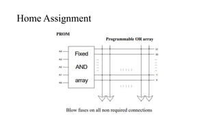
- 16. Home Assignment
- 17. Home Assignment
- 18. EPROM • An EPROM is an erasable PROM. • Unlike an ordinary PROM, an EPROM can be reprogrammed if an existing program in the memory array is erased first. • Assignment : Complete the note
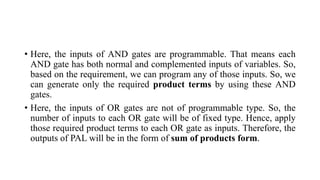
- 19. Programmable Array Logic (PAL) • PAL is a programmable logic device that has Programmable AND array & fixed OR array. • The advantage of PAL is that we can generate only the required product terms of Boolean function instead of generating all the min terms by using programmable AND gates. • The block diagram of PAL is shown in the following figure.
- 20. • Here, the inputs of AND gates are programmable. That means each AND gate has both normal and complemented inputs of variables. So, based on the requirement, we can program any of those inputs. So, we can generate only the required product terms by using these AND gates. • Here, the inputs of OR gates are not of programmable type. So, the number of inputs to each OR gate will be of fixed type. Hence, apply those required product terms to each OR gate as inputs. Therefore, the outputs of PAL will be in the form of sum of products form.
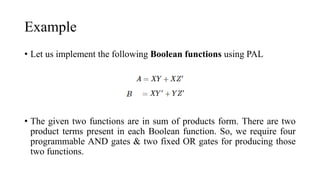
- 21. Example • Let us implement the following Boolean functions using PAL • The given two functions are in sum of products form. There are two product terms present in each Boolean function. So, we require four programmable AND gates & two fixed OR gates for producing those two functions.
- 23. • The programmable AND gates have the access of both normal and complemented inputs of variables. • So, program only the required literals in order to generate one product term by each AND gate. The symbol ‘X’ is used for programmable connections. • Here, the inputs of OR gates are of fixed type. So, the necessary product terms are connected to inputs of each OR gate. So that the OR gates produce the respective Boolean functions. The symbol ‘.’ is used for fixed connections.
- 24. Assignment • Implementation of full adder using PAL
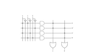
- 25. Programmable Logic Array (PLA) • PLA is a programmable logic device that has both Programmable AND array & Programmable OR array. • Hence, it is the most flexible PLD. • The block diagram of PLA is shown in the following figure.
- 26. • Here, the inputs of AND gates are programmable. That means each AND gate has both normal and complemented inputs of variables. So, based on the requirement, we can program any of those inputs. So, we can generate only the required product terms by using these AND gates. • Here, the inputs of OR gates are also programmable. So, we can program any number of required product terms, since all the outputs of AND gates are applied as inputs to each OR gate. Therefore, the outputs of PAL will be in the form of sum of products form.
- 27. Example • Let us implement the following Boolean functions using PLA. • The given two functions are in sum of products form. The number of product terms present in the given Boolean functions A & B are two and three respectively. One product term, is common in each function. • So, we require four programmable AND gates & two programmable OR gates for producing those two functions.
- 29. • The programmable AND gates have the access of both normal and complemented inputs of variables. So, program only the required literals in order to generate one product term by each AND gate. • All these product terms are available at the inputs of each programmable OR gate. But, only program the required product terms in order to produce the respective Boolean functions by each OR gate. The symbol ‘X’ is used for programmable connections.
- 30. Implement using PAL & PLA
- 31. Assignment • Difference between PLA, PAL and PROM