Programming the ARM CORTEX M3 based STM32F100RBT6 Value Line Discovery Board
15 likes8,213 views

This programming manual is providing the complete details of programming the STM32 Value-line discovery (a low-cost) evaluation board for Value-line of STM32 microcontrollers from STMicroelectronics.


![Complete source code:
//=============================================================================
// STM32VLDISCOVERY tutorial
// Lesson 6. USART.
// Copyright: Gaurav Verma, Assistant Professor, ECE Department.
// Jaypee Institute of Information Technology, Sector-62, Noida.
// e-mail : gaurav.iitkg@gmail.com
// Mobile No.: 9811506739
//=============================================================================
#include "stm32f10x.h"
#include "antilib_gpio.h"
//=============================================================================
// Defines
//=============================================================================
#define USART_RX_GPIO GPIOA
#define USART_RX_PIN 10
#define USART_TX_GPIO GPIOA
#define USART_TX_PIN 9
uint8_t text [] = "STM32VLDISCOVERY/nrnr";
//=============================================================================
//
//=============================================================================
void USART_PutChar(uint8_t ch)
{
while(!(USART1->SR & USART_SR_TXE));
USART1->DR = ch;
}
//=============================================================================](https://image.slidesharecdn.com/programmingthearmcortex-140408120952-phpapp02/85/Programming-the-ARM-CORTEX-M3-based-STM32F100RBT6-Value-Line-Discovery-Board-42-320.jpg)


![ADC_SAMPLE_TIME3(SAMPLE_TIME_239_5) ; // sample time for fourth channel in sequence
Variable for storing conversion values :
vu16 AIN[4]; // 4 locations
DMA configuration
Before we use DMA for transferring data between two areas of memory space of STM32
microcontroller, we have to say to DMA peripheral some informations, like as : source address
(data register of ADC), destination address (table for conversions results), number of transfers
(amount of scanned input channels).
DMA1_Channel1->CPAR = (uint32_t)(&(ADC1->DR)); // peripheral (source) address
DMA1_Channel1->CMAR = (uint32_t)AIN; // memory (destination) address
DMA1_Channel1->CNDTR = 4; // 4 transfers
DMA1_Channel1->CCR |= DMA_CCR1_CIRC | // circular mode enable
DMA_CCR1_MINC | // memory increment mode enable
DMA_CCR1_MSIZE_0 | // memory size 16 bits
DMA_CCR1_PSIZE_0; // peripheral size 16 bits
DMA1_Channel1->CCR |= DMA_CCR1_EN ; // Enable channel
Sending conversion results
For sending result we use code from lesson 8.
do{
sprintf(str, "0:%dtt1:%dtt2:%dtt3:%dr", AIN[0], AIN[1], AIN[2], AIN[3]);
USART_PutString(str);
for(dly = 0; dly < 1000000; dly++);
}while(1);](https://image.slidesharecdn.com/programmingthearmcortex-140408120952-phpapp02/85/Programming-the-ARM-CORTEX-M3-based-STM32F100RBT6-Value-Line-Discovery-Board-46-320.jpg)


More Related Content
What's hot (20)
Viewers also liked (12)


Similar to Programming the ARM CORTEX M3 based STM32F100RBT6 Value Line Discovery Board (20)


Recently uploaded (20)


Programming the ARM CORTEX M3 based STM32F100RBT6 Value Line Discovery Board
- 1. STM32F100RB (ARM Cortex core) Programming Tutorial Introduction STM32VLDISCOVERY evaluation board STM32 Value-line discovery board is a low-cost evaluation board for Value-line of STM32 microcontrollers from STMicroelectronics. Value line of STM32 microcontrollers are low cost version of higher devices. It can run on 24MHz and don’t have some of peripherals available on higher devices. On this board is soldered 64-pin value-line STM32 (with ARM Cortex-M3 core) microcontroller and ST-Link debugger, so board is complete hardware needed to run programs for STM32 devices! You only need USB cable for connection board to PC. Of course, we need build some external hardware because on the STM32LVDISCOVERY are mounted only two LEDs and two pushbuttons - one for RESET and one for user application purposes. Discovery board has two long rows of pin headers and one short (between them) with all important signals from microcontroller and power supply voltages. Due to this short connector STM32VLDISCOVERY board cannot be placed on typical solder less board. This tutorial shows you how to write applications for STM32 devices without use STM32 StdPeriph Library. This library in my opinion isn't best solution for writing apps for STM32 and I show you that writing apps without this library is easy and fun. Although this tutorial is based on STM32 Value Line micros and STM32VLDISCOVERY board in most cases can be also used for other STM32F1 (mainstream) devices and other development boards.
- 2. Lesson 1 - First program. Blinking LED For writing applications for STM32VLDISCOVERY board we need toolchain, which supports STLink debugger and SWD protocol. Unfortunately at this moment OpenOCD debug tool do not support SWD and STLink, so we can't use free tool chains. SWD protocol supports following tool chains: MDK-ARM from Keil, EWARM from IAR and TrueSTUDIO form Atollic. In this tutorial all examples will be shown for MDK-ARM. Creating uVision project - step by step To create new uVision project select "New uVision Project" command from menu "Project": You will be asked for name and disk location for created project. Next, you must select device. On STM32VLDISCOVERY board is installed STM32F100RBT6 device, so select "STM32F100RB" option from dialog window:
- 3. After device selection uVision ask if add startup file to project tree: If you click "Yes", in project tree will be present startup file, suitable for STM32F100RB microcontroller: After creating project, we can write application code. For this we must create a new C source file. From "File" menu select "New" command:
- 4. After this will be created a new text file: Now, let save this file as main.c:
- 5. And add it to project tree: and pick main.c file from disk. File main.c should be in SourceGroup1:
- 6. We are ready to writing application source code. Let us write in main.c file following lines: #include "stm32f10x.h" int main(void) { do{ }while(1); } Save the file and select command "Build target" from "Project" menu. In the "Build output" window will be written following messages: Build target 'Target 1' assembling startup_stm32f10x_md_vl.s... compiling main.c... C:KeilARMINCSTSTM32F10xstm32f10x.h(80): error: #35: #error directive: "Please select first the target STM32F10x device used in your application (in stm32f10x.h file)" Target not created Note: We must defined, which type of STM32 microcontroller are used. So, go to the project tree and click right mouse button on "Target1" folder icon, and select "Options for Target..." command from context menu:
- 7. Next, go to "C/C++" tab and write in "Define" edit box "STM32F10X_MD_VL" string:
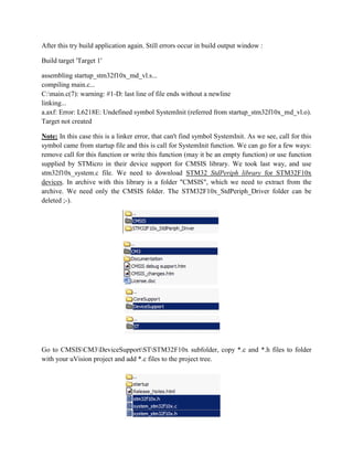
- 8. After this try build application again. Still errors occur in build output window : Build target 'Target 1' assembling startup_stm32f10x_md_vl.s... compiling main.c... C:main.c(7): warning: #1-D: last line of file ends without a newline linking... a.axf: Error: L6218E: Undefined symbol SystemInit (referred from startup_stm32f10x_md_vl.o). Target not created Note: In this case this is a linker error, that can't find symbol SystemInit. As we see, call for this symbol came from startup file and this is call for SystemInit function. We can go for a few ways: remove call for this function or write this function (may it be an empty function) or use function supplied by STMicro in their device support for CMSIS library. We took last way, and use stm32f10x_system.c file. We need to download STM32 StdPeriph library for STM32F10x devices. In archive with this library is a folder "CMSIS", which we need to extract from the archive. We need only the CMSIS folder. The STM32F10x_StdPeriph_Driver folder can be deleted ;-). Go to CMSISCM3DeviceSupportSTSTM32F10x subfolder, copy *.c and *.h files to folder with your uVision project and add *.c files to the project tree.
- 9. Now, try to build project. In "Build output window should be written following text: Build target 'Target 1' assembling startup_stm32f10x_md_vl.s... compiling main.c... compiling system_stm32f10x.c... linking... Program Size: Code=808 RO-data=320 RW-data=20 ZI-data=1636 "prj1.axf" - 0 Error(s), 0 Warning(s). SUCCES! We have first compiled application for STM32! Let’s Blink LED After successfully creating and compiling first empty project we can add some source code to them. We want to blink LED LD4, which are connected to PC8 pin of STM32F100RBT6. So we need to configure this pin as output. At this moment, You need to download from STMicro website document called RM0041. In this Reference Manual are described all peripherals of STM32F100 microcontrollers. Because this document has over 650 pages it impossible to copy all informations to this website. So I will reference to this document and suitable chapters concerning peripherals used in this tutorial. I will not reference to exact page, because after updating document by ST Micro page numbers can be not actual. I will be referenced to sections, figures and tables. RCC configuration Look at section 6 of RM0041, that concern about RCC (Reset and Clock Control) peripheral. In section 6.2 Figure 8 shows clock tree on STM32F100 low and medium density microcontrollers. Looks complicated, but almost all configurations are done by SystemInit function from system_stm32f10x.c file. Clocks will be configured to obtain specified core speed. Remember that - after reset all peripherals have disabled clock! So we need enable clock for every used peripheral. Go to section 6.3.7 of Reference Manual. This section describes APB2ENR register of RCC peripheral. This register is responsible for enabling clock signal for peripherals working on APB2 bus. All GPIO peripherals works on APB2 bus, so this register are interesting for us. Bits 2 to 8 are used to enable clock for each GPIO port (form GPIOA to GPIOG). We ned use only GPIOC port, so we need set bit number 4 of APB2ENR register. How do it? Probably You
- 10. think about (1 << 4)? Right? That is wrong! Open document stm32f10x.h and search for bit name - "IOPCEN". You should find some macro definitions, which one from them is: #define RCC_APB2ENR_IOPCEN ((uint32_t)0x00000010) /*!< I/O port C clock enable */ What is it? It's a bitmask for IOPCEN bit! So we don't need bitwise shifting one by pin number, we can use suitable bitmask! So, how will be looks first code line of us application? Probably something like that: #include "stm32f10x.h" int main(void) { RCC_APB2ENR | = RCC_APB2ENR_IOPCEN; do{ }while(1); } But this is wrong. After compiling application, compiler returns following error: main.c(14): error: #20: identifier "RCC_APB2ENR" is undefined Why? We use register name from Reference Manual, so why it is wrong? This is wrong, because all peripherals are divided into structures that hold peripherals registers. These structures are defined in stm32f10x.h file. So go to this file and search for "Peripheral_registers_structures" string. You will see some of typedefs describing structures for all of peripherals. Each structure holds all registers of peripheral. Naming scheme of peripheral structures are following: PeriphName_TypeDef. So for RCC peripheral structure definitions with registers are "RCC_TypeDef". So let's search for "RCC_TypeDef" string. We see, that registers name are slightly different from names from Reference Manual. Names in structure are without part of peripheral name. Register described in Reference Manual as RCC_APB2ENR in structure has name APB2ENR. OK, now we need name of structure variable. So let search again for RCC_TypeDef string. You should find following line: #define RCC ((RCC_TypeDef *) RCC_BASE) Now all are clear! In stm32f10x.h file is defined macro RCC that in fact are pointer dereference to our RCC_TypeDef structure that resides at RCC_BASE address. If you search for RCC_BASE string, you find another macro, that defines RCC_BASE as base address of RCC peripheral in STM32F100 memory space. So now, we can use RCC macro as pointer to
- 11. structure, that holds all register of RCC peripheral. Now we can write correct code for set IOPCEN bit in APB2ENR register of RCC peripheral: #include "stm32f10x.h" int main(void) { RCC->APB2ENR |= RCC_APB2ENR_IOPCEN; do{ }while(1); } Try to build application. Hooray! No errors! We have enabled clock for GPIOC peripheral and we can configure GPIO for driving LED. GPIO configuration Now, go to Section 7 of RM0041. As you can read, each GPIO port has several registers to configure and control input and output state of microcontroller pins. Most important information for us is that each GPIO port has two 32-bit configuration registers: CRL and CRH. CRL register is responsible for configuration of pins from 0 to 7 and CRH register is responsible for configuration of pins form 8 to 15. So for each GPIO pin we have four configuration bits. Table 16 from RM0041 shows all possible configurations of GPIO pins. Because configuration registers are slightly complicated, I prepared some macros for easier configuring GPIO ports on STM32 microcontrollers. With this macros pin configuration are easy and clear to read. These macros are in antilib_gpio.h file. Download this file, and save into folder with your application project. Example configuration for PC8 pin that works as output looks like that: GPIOC->CRH = (GPIOC->CRH & CONFMASKH(8)) | GPIOPINCONFH(8, GPIOCONF(GPIO_MODE_OUTPUT2MHz, GPIO_CNF_OUTPUT_PUSHPULL)); Let me describe each element of this code line. GPIO->CRH mean of course access to GPIOC_CRH register. We want change configuration only for PC8, so remaining bits of this register should be unchanged. We realize that by reading contents of GPIO_CRH register and clear bits responsible for PC8 configuration. Macro CONFMASKH (8) give bitmask for clearing 4 lowest bits: 0xFFFFFFF0. Clearing this 4 bits will be done by bitwise AND of register with this bitmask. Next, we need to set configuration bits for PC8 suitable for driving LED. Output
- 12. should be work as push-pull output. And what is this megahertz? This specified slew rate on outputs pin. For driving LED we don’t need fast edges of driving signals, so we use slowest slew ratio for PC8. Controlling output state of GPIO pins can be realized on two ways: by writing port value to ODR (Output Data Register) register or by writing to BSRR (Bit Set/Reset Register) or BRR (Bit Reset Register). Writing to ODR register modifies value of all pins of given GPIO port. Writing to BSRR/BRR registers modifies state only this bits, that writing value has ones on bits position. For example to set bit PC8 we can use following code: GPIOC->BSRR = (1 << 8); After execution of this line bit number 8 (and only this bit) of GPIOC will be set. Other bits remain unchanged. Upper 16 bits of BSRR register can be used to clearing pin state: GPIOC->BSRR = (1 << 24); After execution of this line bit number 8 of GPIOC will be cleared. To resetting pin state we can use BRR register too: GPIOC->BRR = (1 << 8); After execution of this line, bit number 8 will be cleared. If we want clear single bit using ODR register, we must perform bitwise logical operations in Read-Modify-Write scheme: GPIOC->ODR = GPIOC->ODR | (1 << 8); but this operation is not atomic! After reading ODR state, his value can be changed (in interrupt for example), and after write modified value we can lose this change. So better use atomic operations with BSRR / BRR register. Finally, let's blink the LED! After getting all informations from above discussion, we can write our blinking LED application. How to make a delay? Simplest way to make a delay (let's call 'monkey delay') is loop counting some many times. Time of this delay it's hard to define. Especially on ARM devices counting how CPU cycles loop will be executed is difficult. Let's define variable named dly:
- 13. volatile uint32_t dly; Short explain about two keywords before variable name. An 'volatile' keyword says to compiler "Don't optimize access to this variable. Its value can change in any time of execution of program". Second keyword defines size of variable - 32-bit unsigned integer. Now, let's do a simple loop using this variable: for(dly = 0; dly < 500000; dly++); This code give us 500.000 loop cycles, that in effect give us some time of CPU spending in the loop. Without keyword 'volatile' this code probably gives us no cycles and no time delay. Complete code of blink LED application: //============================================================================= // STM32VLDISCOVERY tutorial // Lesson 1. Blinking the LED. // Copyright : Gaurav Verma, Assistant Professor, ECE Department. // Jaypee Institute of Information Technology, Sector-62, Noida. // e-mail : [email protected] // Mobile No.: 9811506739 //============================================================================= #include "stm32f10x.h" #include "antilib_gpio.h" //============================================================================= // main function //============================================================================= int main(void) { volatile uint32_t dly; RCC->APB2ENR |= RCC_APB2ENR_IOPCEN; GPIOC->CRH = (GPIOC->CRH & CONFMASKH(8)) | GPIOPINCONFH(8, GPIOCONF(GPIO_MODE_OUTPUT2MHz, GPIO_CNF_OUTPUT_PUSHPULL));
- 14. while (1) { for(dly = 0; dly < 500000; dly++); GPIOC->BSRR = (1 << 8); for(dly = 0; dly < 500000; dly++); GPIOC->BRR = (1 << 8); } } //============================================================================= // End of file //============================================================================= How to make this code more universal? When LED diode will be connected to other pin, we need modify in code all references to them. So let's use the preprocessor to define some macros describing connected LED diode: #define LED_BLUE_GPIO GPIOC #define LED_BLUE_PIN 8 Now we can use defined macros in place to direct GPIO and pin number, but in case of configure GPIO there is need to specify configuration register (low or high). We can do this like in example: #if (LED_BLUE_PIN > 7) LED_BLUE_GPIO->CRH = (LED_BLUE_GPIO->CRH & CONFMASKH(LED_BLUE_PIN)) |GPIOPINCONFH(LED_BLUE_PIN,GPIOCONF(GPIO_MODE_OUTPUT2MHz, GPIO_CNF_OUTPUT_PUSHPULL)); #else LED_BLUE_GPIO->CRL = (LED_BLUE_GPIO->CRL & CONFMASKL(LED_BLUE_PIN)) | GPIOPINCONFL(LED_BLUE_PIN, GPIOCONF(GPIO_MODE_OUTPUT2MHz, GPIO_CNF_OUTPUT_PUSHPULL));
- 15. #endif The #if is preprocessor conditional directive, not the C language conditional instruction, so before compilation the preprocessor depending on value of LED_BLUE_PIN choose proper source code line and place them on source code file that will be compiled. Now, to turn LED on we can use following sequence: GPIOC->BSRR = (1 << LED_BLUE_PIN); and for turn led OFF : GPIOC->BRR = (1 << LED_BLUE_PIN); Complete source code : //============================================================================= // STM32VLDISCOVERY tutorial // Lesson 1. Blinking the LED. // Copyright : Gaurav Verma, Assistant Professor, ECE Department. // Jaypee Institute of Information Technology, Sector-62, Noida. // e-mail : [email protected] // Mobile No.: 9811506739 //============================================================================= #include "stm32f10x.h" #include "antilib_gpio.h" //============================================================================= // Defines //============================================================================= #define LED_BLUE_GPIO GPIOC #define LED_BLUE_PIN 8 //============================================================================= // main function
- 16. //============================================================================= int main(void) { volatile uint32_t dly; RCC->APB2ENR |= RCC_APB2ENR_IOPCEN; #if (LED_BLUE_PIN > 7) LED_BLUE_GPIO->CRH = (LED_BLUE_GPIO->CRH & CONFMASKH(LED_BLUE_PIN)) | GPIOPINCONFH(LED_BLUE_PIN, GPIOCONF(GPIO_MODE_OUTPUT2MHz, GPIO_CNF_OUTPUT_PUSHPULL)); #else LED_BLUE_GPIO->CRL = (LED_BLUE_GPIO->CRL & CONFMASKL(LED_BLUE_PIN)) | GPIOPINCONFL(LED_BLUE_PIN, GPIOCONF(GPIO_MODE_OUTPUT2MHz, GPIO_CNF_OUTPUT_PUSHPULL)); #endif while (1) { for(dly = 0; dly < 300000; dly++); LED_BLUE_GPIO->BSRR = (1 << LED_BLUE_PIN); for(dly = 0; dly < 300000; dly++); LED_BLUE_GPIO->BRR = (1 << LED_BLUE_PIN); } } //============================================================================= // End of file //=============================================================================
- 17. Lesson2. Reading the button After blinking the LED, described in lesson 1, we can do another exercise - reading the button state. On the STM32VLDISCOVERY board we have two buttons - one for resetting board (RST, black) and one for user purpose (USER, blue). The USER button is connected to PA0 pin and active states are high. Creating project is similar to described in lesson 1. First thing to do to use this button is enable clock for GPIO peripheral: RCC->APB2ENR |= RCC_APB2ENR_IOPAEN | RCC_APB2ENR_IOPCEN; Remember that we use also GPIOC, so we need turn on clock for both GPIOA and GPIOC. Next, let's do some defines for USER button: #define SW_USER_GPIO GPIOA #define SW_USER_PIN 0 and now we can configure GPIO to work as input: #if (SW_USER_PIN > 7) SW_USER_GPIO->CRH = (SW_USER_GPIO->CRH & CONFMASKH(SW_USER_PIN)) | GPIOPINCONFH(SW_USER_PIN, GPIOCONF(GPIO_MODE_INPUT, GPIO_CNF_INPUT_FLOATING)); #else SW_USER_GPIO->CRL = (SW_USER_GPIO->CRH & CONFMASKL(SW_USER_PIN)) | GPIOPINCONFL(SW_USER_PIN, GPIOCONF(GPIO_MODE_INPUT, GPIO_CNF_INPUT_FLOATING)); #endif Now we can check in endless loop state of the button and turn LED on if is pressed: while (1) { if(SW_USER_GPIO->IDR & (1 << SW_USER_PIN)) LED_BLUE_GPIO->BSRR = (1 << LED_BLUE_PIN); else
- 18. LED_BLUE_GPIO->BRR = (1 << LED_BLUE_PIN); } Complete code of example: //============================================================================= // STM32VLDISCOVERY tutorial // Lesson 2. Reading from the switch. // Copyright : Gaurav Verma, Assistant Professor, ECE Department. // Jaypee Institute of Information Technology, Sector-62, Noida. // e-mail : [email protected] // Mobile No.: 9811506739 //============================================================================= #include "stm32f10x.h" #include "antilib_gpio.h" //============================================================================= // Defines //============================================================================= #define LED_BLUE_GPIO GPIOC #define LED_BLUE_PIN 8 #define SW_USER_GPIO GPIOA #define SW_USER_PIN 0 //============================================================================= // main function //============================================================================= int main(void) { RCC->APB2ENR |= RCC_APB2ENR_IOPAEN | RCC_APB2ENR_IOPCEN;
- 19. #if (LED_BLUE_PIN > 7) LED_BLUE_GPIO->CRH = (LED_BLUE_GPIO->CRH & CONFMASKH(LED_BLUE_PIN)) | GPIOPINCONFH(LED_BLUE_PIN, GPIOCONF(GPIO_MODE_OUTPUT2MHz, GPIO_CNF_OUTPUT_PUSHPULL)); #else LED_BLUE_GPIO->CRL = (LED_BLUE_GPIO->CRL & CONFMASKL(LED_BLUE_PIN)) | GPIOPINCONFL(LED_BLUE_PIN, GPIOCONF(GPIO_MODE_OUTPUT2MHz, GPIO_CNF_OUTPUT_PUSHPULL)); #endif #if (SW_USER_PIN > 7) SW_USER_GPIO->CRH = (SW_USER_GPIO->CRH & CONFMASKH(SW_USER_PIN)) | GPIOPINCONFH(SW_USER_PIN, GPIOCONF(GPIO_MODE_INPUT, GPIO_CNF_INPUT_FLOATING)); #else SW_USER_GPIO->CRL = (SW_USER_GPIO->CRH & CONFMASKL(SW_USER_PIN)) | GPIOPINCONFL(SW_USER_PIN, GPIOCONF(GPIO_MODE_INPUT, GPIO_CNF_INPUT_FLOATING)); #endif while (1) { if(SW_USER_GPIO->IDR & (1 << SW_USER_PIN)) LED_BLUE_GPIO->BSRR = (1 << LED_BLUE_PIN); else LED_BLUE_GPIO->BRR = (1 << LED_BLUE_PIN); } } //============================================================================= // End of file //=============================================================================
- 20. After flashing MCU and pressing down the USER button blue LED will be turned on, after release the button LED will be turned off. Lesson 3. Blinking with Timer. As i wrote in lesson 1, this is not the best way to make a delay : for(dly = 0; dly < 500000; dly++); CPU wasting time to counting this loop, and also time of delay is hard to define. This kind of delay is maybe good for first program, but not for professional applications. So let's try blinking LED with use one of STM32's timers. Look into section 13 of RM0041 document. This section describes general purpose timers TIM2 to TIM5. These timers are a 16-bit timer with 16-bit prescaler. Now, look into STM32F100RBT6 datasheetto section 3 "Pinouts and pin description". Look for PC8 and PC9 in table 4. As you see, this pin can be connected to channels 3 and 4 of timer TIM3. So let's use in this lesson timer TIM3 to blinking LEDs. Make timer alive First thing which we do is make timer counting. First of all, we need enable clock for timer TIM3: RCC->APB1ENR |= RCC_APB1ENR_TIM3EN; Now, we can configure timer. Let's assume that we want change state of LED each one second. How to do it? You must know input frequency which clocking the timer. Now, look into file system_stm32f10x.c at fragment: #if defined (STM32F10X_LD_VL) || (defined STM32F10X_MD_VL) || (defined STM32F10X_HD_VL) /* #define SYSCLK_FREQ_HSE HSE_VALUE */ #define SYSCLK_FREQ_24MHz 24000000 #else /* #define SYSCLK_FREQ_HSE HSE_VALUE */ /* #define SYSCLK_FREQ_24MHz 24000000 */ /* #define SYSCLK_FREQ_36MHz 36000000 */ /* #define SYSCLK_FREQ_48MHz 48000000 */
- 21. /* #define SYSCLK_FREQ_56MHz 56000000 */ #define SYSCLK_FREQ_72MHz 72000000 #endif As we use Medium Density Value Line microcontroller (MD_VL) we have two options of System Core Clock : equal to HSE (High Speed External source) and 24 MHz Default value in file is SYSCLK_FREQ_24MHz. Based on this macro definition, functions from file system_stm32f10x.c will configure clock system of microcontroller to achieve 24MHz system core clock. So our system frequency is 24MHz. Same frequency clock all peripherals, including timer TIM3. But, how our timer works? In simplest mode timer is counting from 0 to value stored in ARR register, then count again from 0 to ARR. When counter value is equal to ARR the UIF flag in SR register is set. How count one second with this timer? 24MHz of clock give us about 41 nanoseconds of one timer tick. So our timer should count 24 million times to measure one second. But timer is only 16-bits with 16-bits prescaler. Almost like 32-bit timer, but with some limitations. If we don't need high timer resolution we can prescale timer clock, by 24 000 and counting elapsing milliseconds. One second is 1000 milliseconds, so look at code: TIM3->PSC = 23999; // Set prescaler to 24 000 (PSC + 1) TIM3->ARR = 1000; // Auto reload value 1000 TIM3->CR1 = TIM_CR1_CEN;// Enable timer This is the simplest timer configuration. We set prescaler to 24k (remember - prescaler is PSC + 1) and auto reload register to 1000. Next, we enable the timer. From now, timer should be counting. When timer achieve ARR value, the UIF flag will be set. So now we need chceck this flag value, and toggle LED state, when flag is set (counter count to 1000). Code for check flag and toggle LED: if(TIM3->SR & TIM_SR_UIF) { TIM3->SR &= ~TIM_SR_UIF; LED_BLUE_GPIO->ODR ^= (1 << LED_BLUE_PIN);
- 22. } But when check this flag? Now, we check this flag in endless loop: while (1) { if(TIM3->SR & TIM_SR_UIF) { TIM3->SR &= ~TIM_SR_UIF; LED_BLUE_GPIO->ODR ^= (1 << LED_BLUE_PIN); } } Of course, this is not the best way to do this, but at this moment try this. Complete source code : //============================================================================= // STM32VLDISCOVERY tutorial // Lesson 3. Blinking LED with Timer. // Copyright : Gaurav Verma, Assistant Professor, ECE Department. // Jaypee Institute of Information Technology, Sector-62, Noida. // e-mail : [email protected] // Mobile No.: 9811506739 //============================================================================= #include "stm32f10x.h" #include "antilib_gpio.h" //============================================================================= // Defines //============================================================================= #define LED_BLUE_GPIO GPIOC #define LED_BLUE_PIN 8
- 23. //============================================================================= // main function //============================================================================= int main(void) { RCC->APB2ENR |= RCC_APB2ENR_IOPAEN | RCC_APB2ENR_IOPCEN; RCC->APB1ENR |= RCC_APB1ENR_TIM3EN; #if (LED_BLUE_PIN > 7) LED_BLUE_GPIO->CRH = (LED_BLUE_GPIO->CRH & CONFMASKH(LED_BLUE_PIN)) | GPIOPINCONFH(LED_BLUE_PIN, GPIOCONF(GPIO_MODE_OUTPUT2MHz, GPIO_CNF_OUTPUT_PUSHPULL)); #else LED_BLUE_GPIO->CRL = (LED_BLUE_GPIO->CRL & CONFMASKL(LED_BLUE_PIN)) | GPIOPINCONFL(LED_BLUE_PIN, GPIOCONF(GPIO_MODE_OUTPUT2MHz, GPIO_CNF_OUTPUT_PUSHPULL)); #endif TIM3->PSC = 23999; // Set prescaler to 24 000 (PSC + 1) TIM3->ARR = 1000; // Auto reload value 1000 TIM3->CR1 = TIM_CR1_CEN;// Enable timer while (1) { if(TIM3->SR & TIM_SR_UIF) // if UIF flag is set { TIM3->SR &= ~TIM_SR_UIF; // clear UIF flag LED_BLUE_GPIO->ODR ^= (1 << LED_BLUE_PIN); // toggle LED state } } } //============================================================================= // End of file
- 24. //============================================================================= After flashing STM32VLDISCOVERY board blue LED should be change their state each every second. As i wrote - this is not the best way to use timer. The better ways are interrupts, described in next lesson. Lesson4. Blinking with timer interrupts In lesson 3 we use timer TIM3 to measure time for blinking the LED, but shown method was not perfect due to polling timer update flag. In this lesson we learn how to use timer interrupts for blinking LED. STM32 interrupts basics Interrupt system of STM32 microcontrollers are described in section 8.1 of RM0041 document. Now look into startup_stm32f10x_md_vl.s file. At line 61 (or one of their neighborhoods) is defined vector table. This table consists from sequence of DCD (Define Constant Double word) directive. Each of these directives defines address of handler for all interrupts on STM32 microcontroller, except the first element in this table, which is initial value of stack pointer. First sixteen elements are reserved for vectors specific for Cortex-M3 core. Remaining positions can be used by microcontroller vendor for their own interrupts vector. Now look at line 196. There is defined DefauldHandler procedure, some exports functions name with WEAK keyword and similar some of functions label. This is way to define 'default' functions, which are overrided by definite it in other place of application. At line 281 there is only one assembler instruction: B . This is branch instruction to current line. It make endless loop. Now, if we don't define any interrupt handler, all interrupt vectors will be pointed to this branch instruction. This prevents from jumps to undefined locations when not handled interrupt occurs. Thanks to this, we can define vectors only for used interrupts, without modifying vector table each time. How to define our own interrupt handler? It is very simple: void TIM3_IRQHandler(void) { // code of handler }
- 25. When we define our handler, it's address will be placed on proper location in interrupts vectors table. Define vector is one of things to make interrupt working. Next thing is enable interrupt in NVIC (Nested Vectored Interrupt Controller). How do it? Like as this: NVIC_EnableIRQ(TIM3_IRQn); The last thing is enable peripheral to requests interrupt. For our timer we want enable update event to generate an interrupt: TIM3->DIER = TIM_DIER_UIE; Now, we can place in interrupt handler our code for check flag and toggle LED state: void TIM3_IRQHandler(void) { if(TIM3->SR & TIM_SR_UIF) // if UIF flag is set { TIM3->SR &= ~TIM_SR_UIF; // clear UIF flag LED_BLUE_GPIO->ODR ^= (1 << LED_BLUE_PIN); // toggle LED state } } Remember, interrupt flag must be cleared after enter to interrupt handler. Otherwise, interrupt handler will be still executed. Complete source code: //============================================================================= // STM32VLDISCOVERY tutorial // Lesson 4. Blinking LED with Timer Interrupt. // Copyright: Gaurav Verma, Assistant Professor, ECE Department. // Jaypee Institute of Information Technology, Sector-62, Noida. // e-mail : [email protected]
- 26. // Mobile No.: 9811506739 //============================================================================= #include "stm32f10x.h" #include "antilib_gpio.h" //============================================================================= // Defines //============================================================================= #define LED_BLUE_GPIO GPIOC #define LED_BLUE_PIN 8 //============================================================================= // main function //============================================================================= int main(void) { RCC->APB2ENR |= RCC_APB2ENR_IOPAEN | RCC_APB2ENR_IOPCEN; RCC->APB1ENR |= RCC_APB1ENR_TIM3EN; #if (LED_BLUE_PIN > 7) LED_BLUE_GPIO->CRH = (LED_BLUE_GPIO->CRH & CONFMASKH(LED_BLUE_PIN)) | GPIOPINCONFH(LED_BLUE_PIN, GPIOCONF(GPIO_MODE_OUTPUT2MHz, GPIO_CNF_OUTPUT_PUSHPULL)); #else LED_BLUE_GPIO->CRL = (LED_BLUE_GPIO->CRL & CONFMASKL(LED_BLUE_PIN)) | GPIOPINCONFL(LED_BLUE_PIN, GPIOCONF(GPIO_MODE_OUTPUT2MHz, GPIO_CNF_OUTPUT_PUSHPULL)); #endif TIM3->PSC = 23999; // Set prescaler to 24 000 (PSC + 1) TIM3->ARR = 1000; // Auto reload value 1000 TIM3->DIER = TIM_DIER_UIE; // Enable update interrupt (timer level)
- 27. TIM3->CR1 = TIM_CR1_CEN; // Enable timer NVIC_EnableIRQ(TIM3_IRQn); // Enable interrupt from TIM3 (NVIC level) while (1) {} } //============================================================================= // TIM3 Interrupt Handler //============================================================================= void TIM3_IRQHandler(void) { if(TIM3->SR & TIM_SR_UIF) // if UIF flag is set { TIM3->SR &= ~TIM_SR_UIF; // clear UIF flag LED_BLUE_GPIO->ODR ^= (1 << LED_BLUE_PIN); // toggle LED state } } //============================================================================= // End of file //============================================================================= As we see, CPU execute endless loop that do nothing. But LED is blinking. Each every 1000 milliseconds state of LED is changing in the interrupt handler routine.
- 28. Lesson5. Blinking with timer hardware After we successfully blink LED with interrupt from TIM3 we can do next step: blink LED only with hardware - even without any single line of code! Of course, code for timer initialization will be required, but blinking will be realized only by hardware. For do this, we use compare units of timer TIM3. Now, go to section 13.3.8 of RM0041 document. There is described output compare functionality of timer. As you remember from previous lesson, two of discovery board LEDs can be connected to TIM3 channel 3 and 4. To connect LEDs to this channel we must configure PC8 and PC9 pin as alternate function outputs. On PC8 and PC9 timer outputs are available only after remap. So we need do full remap of TIM3 outputs. Now, go to section 7.4.2 of RM0041 document. There are described register MAPR. As You see, to do full remap of TIM3 we need set both bits TIM3_REMAP: AFIO->MAPR = AFIO_MAPR_TIM3_REMAP; // Full TIM3 remap To configure channel output for toggling on CH3 and CH4 output: TIM3->CCMR2 = TIM_CCMR2_OC4M_0 | TIM_CCMR2_OC4M_1 | TIM_CCMR2_OC3M_0 | TIM_CCMR2_OC3M_1; // Toggle output 3 & 4 on compare match Now, we must enable compare on 3 & 4 channel : TIM3->CCER = TIM_CCER_CC4E | TIM_CCER_CC3E; and set compare values : TIM3->CCR3 = 250; // Compare 4 with 250 TIM3->CCR4 = 500; // Compare 4 with 500 Complete source code : //============================================================================= // STM32VLDISCOVERY tutorial // Lesson 5. Blinking LED with Timer Hardware. // Copyright : Gaurav Verma, Assistant Professor, ECE Department. // Jaypee Institute of Information Technology, Sector-62, Noida.
- 29. // e-mail : [email protected] // Mobile No.: 9811506739 //============================================================================= #include "stm32f10x.h" #include "antilib_gpio.h" //============================================================================= // Defines //============================================================================= #define LED_BLUE_GPIO GPIOC #define LED_BLUE_PIN 8 #define LED_GREEN_GPIO GPIOC #define LED_GREEN_PIN 9 //============================================================================= // main function //============================================================================= int main(void) { RCC->APB2ENR |= RCC_APB2ENR_IOPAEN | RCC_APB2ENR_IOPCEN | RCC_APB2ENR_AFIOEN; RCC->APB1ENR |= RCC_APB1ENR_TIM3EN; #if (LED_BLUE_PIN > 7) LED_BLUE_GPIO->CRH = (LED_BLUE_GPIO->CRH & CONFMASKH(LED_BLUE_PIN)) | GPIOPINCONFH(LED_BLUE_PIN, GPIOCONF(GPIO_MODE_OUTPUT2MHz, GPIO_CNF_AFIO_PUSHPULL)); #else
- 30. LED_BLUE_GPIO->CRL = (LED_BLUE_GPIO->CRL & CONFMASKL(LED_BLUE_PIN)) | GPIOPINCONFL(LED_BLUE_PIN, GPIOCONF(GPIO_MODE_OUTPUT2MHz, GPIO_CNF_AFIO_PUSHPULL)); #endif #if (LED_GREEN_PIN > 7) LED_GREEN_GPIO->CRH = (LED_GREEN_GPIO->CRH & CONFMASKH(LED_GREEN_PIN)) | GPIOPINCONFH(LED_GREEN_PIN, GPIOCONF(GPIO_MODE_OUTPUT2MHz, GPIO_CNF_AFIO_PUSHPULL)); #else LED_GREEN_GPIO->CRL = (LED_GREEN_GPIO->CRL & CONFMASKL(LED_GREEN_PIN)) | GPIOPINCONFL(LED_GREEN_PIN, GPIOCONF(GPIO_MODE_OUTPUT2MHz, GPIO_CNF_AFIO_PUSHPULL)); #endif AFIO->MAPR = AFIO_MAPR_TIM3_REMAP; // Full TIM3 remap TIM3->PSC = 23990; // Set prescaler to 24 000 (PSC + 1) TIM3->ARR = 500; // Auto reload value 500 TIM3->CCR3 = 250; // Compare 4 with 250 TIM3->CCR4 = 500; // Compare 4 with 500 TIM3->CCMR2 = TIM_CCMR2_OC4M_0 | TIM_CCMR2_OC4M_1 | TIM_CCMR2_OC3M_0 | TIM_CCMR2_OC3M_1; // Toggle output 3 & 4 on compare match TIM3->CCER = TIM_CCER_CC4E | TIM_CCER_CC3E; // Enable compare output 3 & 4 TIM3->CR1 = TIM_CR1_CEN; // Enable timer while (1) {} } //============================================================================= // End of file //=============================================================================
- 31. After flashing MCU both LEDs will be blinking with 500ms period with 250ms delay between blue and green. And no code in endless loop and no interrupt! Lesson6. Pulse Width Modulation (PWM) In lesson 5 we learn how to blink led with Compare unit of timer TIM3. Compare unit can be also used in pulse width modulation mode for brightness control of LED. Now, go to section number 13.3.9 of RM0041 document. Different PWM duty Configuration of compare module is slightly different from previous example: TIM3->CCMR2 = TIM_CCMR2_OC4M_2 | TIM_CCMR2_OC4M_1 | TIM_CCMR2_OC3M_2 | TIM_CCMR2_OC3M_1; // PWM mode on channel 3 & 4 Now, CCR3 and CCR4 registers holds PWM duty value. Write initial duty value to registers: TIM3->CCR3 = 0; // Start PWM duty for channel 3 TIM3->CCR4 = 500; // Start PWM duty for channel 4 Each time when timer reloads new value we want to change current PWM duty in both channels. So in interrupt handler from TIM3 we well be change duty on both channels. On CH3 we increase duty by 1% each time, on CH4 we decrease duty by 1% each time: void TIM3_IRQHandler(void) { if(TIM3->SR & TIM_SR_UIF) // if UIF flag is set { TIM3->SR &= ~TIM_SR_UIF; // clear UIF flag TIM3->CCR3 += 5; // increase ch3 duty if(TIM3->CCR3 == 500) // if maximum TIM3->CCR3 = 0; // set to zero
- 32. TIM3->CCR4 -= 5; // decrease ch4 duty if(TIM3->CCR4 == 0) // if minimum TIM3->CCR4 = 500; // set to maximum } } Complete source code : //============================================================================= // STM32VLDISCOVERY tutorial // Lesson 6. Pulse Width Modulation. // Copyright: Gaurav Verma, Assistant Professor, ECE Department. // Jaypee Institute of Information Technology, Sector-62, Noida. // e-mail : [email protected] // Mobile No.: 9811506739 //============================================================================= #include "stm32f10x.h" #include "antilib_gpio.h" //============================================================================= // Defines //============================================================================= #define LED_BLUE_GPIO GPIOC #define LED_BLUE_PIN 8 #define LED_GREEN_GPIO GPIOC #define LED_GREEN_PIN 9 //============================================================================= // main function //=============================================================================
- 33. int main(void) { RCC->APB2ENR |= RCC_APB2ENR_IOPCEN | RCC_APB2ENR_AFIOEN; RCC->APB1ENR |= RCC_APB1ENR_TIM3EN; #if (LED_BLUE_PIN > 7) LED_BLUE_GPIO->CRH = (LED_BLUE_GPIO->CRH & CONFMASKH(LED_BLUE_PIN)) | GPIOPINCONFH(LED_BLUE_PIN, GPIOCONF(GPIO_MODE_OUTPUT2MHz, GPIO_CNF_AFIO_PUSHPULL)); #else LED_BLUE_GPIO->CRL = (LED_BLUE_GPIO->CRL & CONFMASKL(LED_BLUE_PIN)) | GPIOPINCONFL(LED_BLUE_PIN, GPIOCONF(GPIO_MODE_OUTPUT2MHz, GPIO_CNF_AFIO_PUSHPULL)); #endif #if (LED_GREEN_PIN > 7) LED_GREEN_GPIO->CRH = (LED_GREEN_GPIO->CRH & CONFMASKH(LED_GREEN_PIN)) | GPIOPINCONFH(LED_GREEN_PIN, GPIOCONF(GPIO_MODE_OUTPUT2MHz, GPIO_CNF_AFIO_PUSHPULL)); #else LED_GREEN_GPIO->CRL = (LED_GREEN_GPIO->CRL & CONFMASKL(LED_GREEN_PIN)) | GPIOPINCONFL(LED_GREEN_PIN, GPIOCONF(GPIO_MODE_OUTPUT2MHz, GPIO_CNF_AFIO_PUSHPULL)); #endif AFIO->MAPR = AFIO_MAPR_TIM3_REMAP; // Full TIM3 remap TIM3->PSC = 239; // Set prescaler to 24 000 (PSC + 1) TIM3->ARR = 500; // Auto reload value 500 TIM3->CCR3 = 0; // Start PWM duty for channel 3 TIM3->CCR4 = 500; // Start PWM duty for channel 4
- 34. TIM3->CCMR2 = TIM_CCMR2_OC4M_2 | TIM_CCMR2_OC4M_1 | TIM_CCMR2_OC3M_2 | TIM_CCMR2_OC3M_1; // PWM mode on channel 3 & 4 TIM3->CCER = TIM_CCER_CC4E | TIM_CCER_CC3E; // Enable compare on channel 3 & 4 TIM3->CR1 = TIM_CR1_CEN; // Enable timer TIM3->DIER = TIM_DIER_UIE; // Enable update interrupt (timer level) NVIC_EnableIRQ(TIM3_IRQn); // Enable interrupt from TIM3 (NVIC level) while (1) {} } //============================================================================= // TIM3 Interrupt Handler //============================================================================= void TIM3_IRQHandler(void) { if(TIM3->SR & TIM_SR_UIF) // if UIF flag is set { TIM3->SR &= ~TIM_SR_UIF; // clear UIF flag TIM3->CCR3 += 5; // increase ch3 duty if(TIM3->CCR3 == 500) // if maximum TIM3->CCR3 = 0; // set to zero TIM3->CCR4 -= 5; // decrease ch4 duty if(TIM3->CCR4 == 0) // if minimum TIM3->CCR4 = 500; // set to maximum } } //============================================================================= // End of file //=============================================================================
- 35. Lesson 7 Analog to digital converter (ADC) Every STM32 microcontroller has at least one 12-bit analog to digital converter. In STM32F100RBT6 microcontroller there are one ADC with 16 input channels. In this example we use one of analog input of MCU to control PWM duty of LED brightness (described in lesson 6). Now, we must connect external potentiometer to STM32VLDISCOVERY board like on the schematic. ADC peripheral is described in section 10 of RM0041 document. So read this section now. Now, I will introduce next part of "AntiLib" project: antilib_adc.h. In this file are some intuitive macros for easier configuration of ADC peripheral. There are macros that define sample time: #define SAMPLE_TIME_1_5 0 #define SAMPLE_TIME_7_5 1 #define SAMPLE_TIME_13_5 2 #define SAMPLE_TIME_28_5 3 #define SAMPLE_TIME_41_5 4 #define SAMPLE_TIME_55_5 5 #define SAMPLE_TIME_71_5 6 #define SAMPLE_TIME_239_5 7 and shifting macros for each channel : #define ADC_SAMPLE_TIME0(x) (x << 0) #define ADC_SAMPLE_TIME9(x) (x << 27) #define ADC_SAMPLE_TIME10(x) (x << 0) #define ADC_SAMPLE_TIME17(x) (x << 21) With this macros configuration of sample time for channels are clear and readable: ADC1->SMPR2 = ADC_SAMPLE_TIME0(SAMPLE_TIME_239_5); To define length of sequence is prepared macro:
- 36. #define ADC_SEQUENCE_LENGTH(x) (x << 20) This macro shift macro parameter by 20 bits. Sequence lenght is numbered from 0. For only one channel in sequence configuration looks like this : ADC1->SQR1 = ADC_SEQUENCE_LENGTH(0); // One channel in sequence I'm prepare also macros for definig each sequence channels : // SQR3 #define ADC_SEQ1(x) (x << 0) #define ADC_SEQ2(x) (x << 5) #define ADC_SEQ6(x) (x << 25) // SQR2 #define ADC_SEQ7(x) (x << 0) #define ADC_SEQ12(x) (x << 25) // SQR1 #define ADC_SEQ13(x) (x << 0) #define ADC_SEQ16(x) (x << 15) Complete configuration of ADC peripheral: ADC1->CR2 = ADC_CR2_ADON | ADC_CR2_CONT; // Turn on ADC, enable continues mode ADC1->SQR1 = ADC_SEQUENCE_LENGTH(0); // One channel in sequence ADC1->SQR3 = ADC_SEQ1(0); // ADC channel 0 is first in sequence ADC1->SMPR2 = ADC_SAMPLE_TIME0(SAMPLE_TIME_239_5); // sample time for first channel ADC1->CR1 = ADC_CR1_EOCIE; // Enable interrupt form End Of Conversion NVIC_EnableIRQ(ADC1_IRQn); // Enable interrupt form ACD1 peripheral ADC1->CR2 |= ADC_CR2_ADON; // Turn on conversion Now we can define handler for interrupt from ADC End of Conversion:
- 37. void ADC1_IRQHandler (void) { if(ADC1->SR & ADC_SR_EOC) { TIM3->CCR3 = ADC1->DR; // Copy value of analog input to PWM duty register } } Complete source code of example: //============================================================================= // STM32VLDISCOVERY tutorial // Lesson 7. Analog to Digital Convertor. // Copyright: Gaurav Verma, Assistant Professor, ECE Department. // Jaypee Institute of Information Technology, Sector-62, Noida. // e-mail : [email protected] // Mobile No.: 9811506739 //============================================================================= #include "stm32f10x.h" #include "antilib_gpio.h" #include "antilib_adc.h" //============================================================================= // Defines //============================================================================= #define LED_BLUE_GPIO GPIOC #define LED_BLUE_PIN 8 #define AIN0_GPIO GPIOA #define AIN0_PIN 0 //=============================================================================
- 38. // main function //============================================================================= int main(void) { RCC->APB2ENR |= RCC_APB2ENR_IOPAEN | RCC_APB2ENR_IOPCEN | RCC_APB2ENR_AFIOEN | RCC_APB2ENR_ADC1EN; RCC->APB1ENR |= RCC_APB1ENR_TIM3EN; #if (LED_BLUE_PIN > 7) LED_BLUE_GPIO->CRH = (LED_BLUE_GPIO->CRH & CONFMASKH(LED_BLUE_PIN)) | GPIOPINCONFH(LED_BLUE_PIN, GPIOCONF(GPIO_MODE_OUTPUT2MHz, GPIO_CNF_AFIO_PUSHPULL)); #else LED_BLUE_GPIO->CRL = (LED_BLUE_GPIO->CRL & CONFMASKL(LED_BLUE_PIN)) | GPIOPINCONFL(LED_BLUE_PIN, GPIOCONF(GPIO_MODE_OUTPUT2MHz, GPIO_CNF_AFIO_PUSHPULL)); #endif #if (AIN0_PIN > 7) AIN0_GPIO->CRH = (AIN0_GPIO->CRH & CONFMASKH(AIN0_PIN)) | GPIOPINCONFH(AIN0_PIN, GPIOCONF(GPIO_MODE_INPUT, GPIO_CNF_INPUT_ANALOG)); #else AIN0_GPIO->CRL = (AIN0_GPIO->CRL & CONFMASKL(AIN0_PIN)) | GPIOPINCONFL(AIN0_PIN, GPIOCONF(GPIO_MODE_INPUT, GPIO_CNF_INPUT_ANALOG)); #endif AFIO->MAPR = AFIO_MAPR_TIM3_REMAP; // Full TIM3 remap TIM3->PSC = 23; // Set prescaler to 24 (PSC + 1) TIM3->ARR = 4096; // Auto reload value 4096 (PWM resolution 12-bits) TIM3->CCR3 = 0; // Start value channel 3
- 39. TIM3->CCMR2 = TIM_CCMR2_OC3M_2 | TIM_CCMR2_OC3M_1; // PWM mode on channel 3 TIM3->CCER = TIM_CCER_CC3E; // Enable compare on channel 3 TIM3->CR1 = TIM_CR1_CEN; // Enable timer ADC1->CR2 = ADC_CR2_ADON | ADC_CR2_CONT; // Turn on ADC, enable continues mode ADC1->SQR1 = ADC_SEQUENCE_LENGTH(0); // One channel in sequence ADC1->SQR3 = ADC_SEQ1(0); // ADC channel 0 is first in sequence ADC1->SMPR2 = ADC_SAMPLE_TIME0(SAMPLE_TIME_239_5); // sample time for first channel ADC1->CR1 = ADC_CR1_EOCIE; // Enable interrupt form End Of Conversion NVIC_EnableIRQ(ADC1_IRQn); // Enable interrupt form ACD1 peripheral ADC1->CR2 |= ADC_CR2_ADON; // Turn on conversion while (1) {} } //============================================================================= // ADC1 Interrupt handler //============================================================================= void ADC1_IRQHandler (void) { if(ADC1->SR & ADC_SR_EOC) { TIM3->CCR3 = ADC1->DR; } } //============================================================================= // End of file //============================================================================= Changing value of analog input should change LED brightness.
- 40. Lesson8. Communication with USART In this lesson i show you the simplest way to use USART for communication with other device (for example your PC). USART configuration USART peripheral is described in section 23 of RM0041 document. There is lot of data to read, but for simple asynchronous communication we don't need read whole chapter. Main features are described in sections from 23.3.1 to 23.3.4. To use USART peripheral we must enable clock for it, and for GPIO used by peripheral. It is obvious, but sometimes easy to forget. USART1, which are used in this lesson, is connected to APB2 bus, and use GPIOA (by default). Code for enable clock for USART1 and GPIOA: RCC->APB2ENR |= RCC_APB2ENR_IOPAEN | RCC_APB2ENR_USART1EN; After enabling clock for USART1 peripheral, we can configure it. What we need to do? At this moment we need two things: enable usart transmitter, and sets baudrate. Enabling transmitter is done by setting UE (USART enable) and TE (transmitter enable) bits in CR1 register of USART1 peripheral : USART1->CR1 = USART_CR1_UE | USART_CR1_TE; In RM0041 document there is shown sophisticated way to calculate USART baudrate. There is mantissa and fractional part of divider, but forget about them! Calculating baudrate is easier than shown in reference manual. So how to calculate value of BRR register? Just divide peripheral clock by baudrate! We want configure USART for communication with transmission speed equal to 115200 bits per second. It’s done by one line : USART1->BRR = (SystemCoreClock / 115200); What is SystemCoreClock? This is variable sets by SystemInit function that holds current system frequency. By default, APB2 bus clock is equal to system frequency; we can use it to calculate baudrate. Sending single character In this lesson I show simplest way to sending data - using pooling. Before write data to DR register, we check state of TXE (transmitter empty) flag. When this flag is clear, we can't write to DR register. High value of this flag mean that is no data in transmit buffer (previous data just be sent or there is first transmission) and we can write new data to send. So let's create function dedicated to sending one byte via USART:
- 41. void USART_PutChar(uint8_t ch) { while(!(USART1->SR & USART_SR_TXE)); USART1->DR = ch; } Sending text When we can send single character we can write function for sending typical for C language null-terminated strings. Null terminated string is character array, that last element has value zero. Empty string has one element - value zero. So before sending character we must check if character has different value than zero. If this condition is true, we can send first character and increment pointer to prepare next character to send. Repeat this in loop until pointer will be pointed to character value zero. void USART_PutString(uint8_t * str) { while(*str != 0) { USART_PutChar(*str); str++; } } Now, we are ready to send text by USART: USART_PutString(text); // argument is pointer variable USART_PutString("Some text to send"); // argument is constant string
- 42. Complete source code: //============================================================================= // STM32VLDISCOVERY tutorial // Lesson 6. USART. // Copyright: Gaurav Verma, Assistant Professor, ECE Department. // Jaypee Institute of Information Technology, Sector-62, Noida. // e-mail : [email protected] // Mobile No.: 9811506739 //============================================================================= #include "stm32f10x.h" #include "antilib_gpio.h" //============================================================================= // Defines //============================================================================= #define USART_RX_GPIO GPIOA #define USART_RX_PIN 10 #define USART_TX_GPIO GPIOA #define USART_TX_PIN 9 uint8_t text [] = "STM32VLDISCOVERY/nrnr"; //============================================================================= // //============================================================================= void USART_PutChar(uint8_t ch) { while(!(USART1->SR & USART_SR_TXE)); USART1->DR = ch; } //=============================================================================
- 43. // //============================================================================= void USART_PutString(uint8_t * str) { while(*str != 0) { USART_PutChar(*str); str++; } } //============================================================================= // main function //============================================================================= int main(void) { vu32 dly; RCC->APB2ENR |= RCC_APB2ENR_IOPAEN | RCC_APB2ENR_USART1EN; #if (USART_RX_PIN > 7) USART_RX_GPIO->CRH = (USART_RX_GPIO->CRH & CONFMASKH(USART_RX_PIN)) | GPIOPINCONFH(USART_RX_PIN, GPIOCONF(GPIO_MODE_INPUT, GPIO_CNF_INPUT_PULLUPDOWN)); #else USART_RX_GPIO->CRL = (USART_RX_GPIO->CRL & CONFMASKL(USART_RX_PIN)) | GPIOPINCONFL(USART_RX_PIN, GPIOCONF(GPIO_MODE_INPUT, GPIO_CNF_INPUT_PULLUPDOWN)); #endif #if (USART_TX_PIN > 7) USART_TX_GPIO->CRH = (USART_TX_GPIO->CRH & CONFMASKH(USART_TX_PIN)) | GPIOPINCONFH(USART_TX_PIN, GPIOCONF(GPIO_MODE_OUTPUT2MHz, GPIO_CNF_AFIO_PUSHPULL)); #else
- 44. USART_TX_GPIO->CRL = (USART_TX_GPIO->CRL & CONFMASKL(USART_TX_PIN)) | GPIOPINCONFL(USART_TX_PIN, GPIOCONF(GPIO_MODE_OUTPUT2MHz, GPIO_CNF_AFIO_PUSHPULL)); #endif USART1->CR1 = USART_CR1_UE | USART_CR1_TE; USART1->BRR = (SystemCoreClock / 115200); while (1) { USART_PutString(text); for(dly = 0; dly < 1000000; dly++); } } //============================================================================= // End of file //============================================================================= Effect of this code:
- 45. Lesson9. Analog to digital converter (ADC) with Direct Memory Access (DMA) In lesson 7 I introduce analog to digital converter, that measure voltage on one analog input. For measure voltage on more than one input the best way is use DMA for automatic transfer data from ADC to memory. Direct memory access is a mechanism that allows to transferring data between memories without usage of CPU. ADC configuration In comparison to ADC configuration from lesson 7, we must enabled two new modes in ADC peripheral: SCAN mode and DMA mode. Scan mode allows for automatic scanning selected channels without interaction from CPU. After conversion of each channel immediately starts new conversion of next channel in sequence. We can scan up to 16 regular channels in the sequence. In scan mode there is risk of overwrite data from previous conversion, because all conversion results are stored in this same data register (DR). For this reason in connection with SCAN mode are used DMA mode, that allows for automatic storage of conversion values in data memory after each conversion. ADC1->CR2 = ADC_CR2_ADON | // turn on ADC ADC_CR2_CONT | // enable continues mode ADC_CR2_DMA; // enable DMA mode ADC1->CR1 = ADC_CR1_SCAN; // enable scan mode Configuration of ADC sequencer: ADC1->SQR1 = ADC_SEQUENCE_LENGTH(3); // four channels in sequence ADC1->SQR3 = ADC_SEQ1(0) | // channel 0 is first in sequence ADC_SEQ2(1) | // channel 1 is second in sequence ADC_SEQ3(2) | // channel 2 is third in sequence ADC_SEQ4(3) ; // channel 3 is fourth in sequence ADC1->SMPR2 = ADC_SAMPLE_TIME0(SAMPLE_TIME_239_5) | // sample time for first channel in sequence ADC_SAMPLE_TIME1(SAMPLE_TIME_239_5) | // sample time for second channel in sequence ADC_SAMPLE_TIME2(SAMPLE_TIME_239_5) | // sample time for third channel in sequence
- 46. ADC_SAMPLE_TIME3(SAMPLE_TIME_239_5) ; // sample time for fourth channel in sequence Variable for storing conversion values : vu16 AIN[4]; // 4 locations DMA configuration Before we use DMA for transferring data between two areas of memory space of STM32 microcontroller, we have to say to DMA peripheral some informations, like as : source address (data register of ADC), destination address (table for conversions results), number of transfers (amount of scanned input channels). DMA1_Channel1->CPAR = (uint32_t)(&(ADC1->DR)); // peripheral (source) address DMA1_Channel1->CMAR = (uint32_t)AIN; // memory (destination) address DMA1_Channel1->CNDTR = 4; // 4 transfers DMA1_Channel1->CCR |= DMA_CCR1_CIRC | // circular mode enable DMA_CCR1_MINC | // memory increment mode enable DMA_CCR1_MSIZE_0 | // memory size 16 bits DMA_CCR1_PSIZE_0; // peripheral size 16 bits DMA1_Channel1->CCR |= DMA_CCR1_EN ; // Enable channel Sending conversion results For sending result we use code from lesson 8. do{ sprintf(str, "0:%dtt1:%dtt2:%dtt3:%dr", AIN[0], AIN[1], AIN[2], AIN[3]); USART_PutString(str); for(dly = 0; dly < 1000000; dly++); }while(1);
- 47. Complete source code: Effect of this on terminal: