SEQUENTIAL LOGIC CIRCUITS (FLIP FLOPS AND LATCHES)
Download as pptx, pdf2 likes395 views
The document presents an overview of sequential circuits, specifically focusing on latches and flip-flops, which are fundamental for data storage in digital electronics. It details various types of latches and flip-flops, including their functionalities, differences, and applications in circuits with respect to synchronous and asynchronous operations. Additionally, it covers the operation of specific types like SR, JK, and D flip-flops, highlighting their construction and behavior with respect to clock signals.
1 of 30
Download to read offline


![SR LATCH ACTIVE HIGH
This SR latch is sometimes referred
as direct coupled RS flipflop.
• In an active high SR Latch two cross
coupled NOR gates are used.
• When the SET input goes high , the
output also goes high.[SET]
• When the SET input returns to low ,
however the output remains
High.[HOLD]
• The output stays High until the
RESET input goes High.
MAJOR PROBLEM:
In an S-R Latch ,activation of S input sets
the circuit, while activation of R input
resets the circuit. If both S and R inputs
are activated simultaneously , the circuit
will be in an invalid condition.
KEY POINT:
Active high is S based when S and R are
contrary to each other.](https://image.slidesharecdn.com/sequentialcircuitsautosaved2-211203041812/85/SEQUENTIAL-LOGIC-CIRCUITS-FLIP-FLOPS-AND-LATCHES-8-320.jpg)

![SR LATCH ACTIVE LOW
• In an active low SR Latch two cross
coupled NAND gates are used.
• When the RESET input goes high ,
the output Q also goes high.[SET]
• When the RESET input returns to low,
the output Q also returns to
low.[RESET]
• When both the inputs are high , then
the
output Q will remains same.[HOLD]
MAJOR PROBLEM:
If both S and R inputs are low , then
the circuit will be in an invalid
condition.
KEY POINT:
Active low is R based when S and R are
contrary to each other.](https://image.slidesharecdn.com/sequentialcircuitsautosaved2-211203041812/85/SEQUENTIAL-LOGIC-CIRCUITS-FLIP-FLOPS-AND-LATCHES-10-320.jpg)


![D FLIP-FLOP
• A D flip flop is by far the most important
of all the clocked flip-flops.
• It is used to create a delay in the circuit.
• It is a modification of SR clocked flipflop
with the addition of an inverter to prevent
S and R inputs from being at the same
logic level.
• The next state of the flip flop is the same
as the D input and is independent of the
present state.
• if the data input is held HIGH the flip flop
would be “SET” and when it is low the
flipflop would change and become
“RESET”.[Clock is 1 for both the
conditions].](https://image.slidesharecdn.com/sequentialcircuitsautosaved2-211203041812/85/SEQUENTIAL-LOGIC-CIRCUITS-FLIP-FLOPS-AND-LATCHES-17-320.jpg)


Ad
Recommended
Register in Digital Logic
Register in Digital LogicISMT College A register is a group of flip-flops that can store multiple bits of data. There are four types of shift registers: serial-in serial-out (SISO), serial-in parallel-out (SIPO), parallel-in serial-out (PISO), and parallel-in parallel-out (PIPO). Shift registers allow data to move between flip-flops on each clock pulse. Ring counters and Johnson counters are examples of shift register counters that produce repeating output sequences.
Binary adder
Binary adderJawaher Abdulwahab Fadhil A half adder is a combinational circuit that performs addition of two binary inputs and has two binary outputs. A full adder performs the addition of three bits, including two input bits and a previous carry bit, and has three inputs and two outputs. Two half adders can be combined using exclusive-OR and AND gates to form a full adder, which is commonly used as a component in cascading adders to add larger binary numbers like 8 or 16 bits.
sequential circuits
sequential circuitsUnsa Shakir Sequential circuits have outputs determined by both the current inputs and previous outputs due to the inclusion of memory elements. Combinational circuits only have outputs determined by the current inputs. Sequential circuits contain logic gates arranged in parallel and feedback loops allowing the circuit to store past states, while combinational circuits only depend on the current input combination. There are different types of sequential circuits including those controlled by a clock signal from a clock generator that produces periodic pulses defining the circuit timing.
SEQUENTIAL CIRCUITS INTRODUCTION
SEQUENTIAL CIRCUITS INTRODUCTIONEasy n Inspire L The document discusses sequential logic circuits, distinguishing them from combinational circuits by emphasizing that sequential circuits rely on both current and previous input for output, unlike combinational circuits that only depend on current inputs. It outlines the types of sequential circuits, namely asynchronous and synchronous circuits, highlighting their characteristics such as the use of clock signals and speed differences. Additionally, it mentions basic components used in constructing sequential circuits, like flip-flops, latches, and counters.
KARNAUGH MAP(K-MAP)
KARNAUGH MAP(K-MAP)mihir jain The document discusses Karnaugh maps (K-maps), which are a tool for representing and simplifying Boolean functions with up to six variables. K-maps arrange the variables in a grid according to their binary values. Adjacent cells that differ in only one variable can be combined to simplify the function by eliminating that variable. The document provides examples of using K-maps to minimize Boolean functions in sum of products and product of sums form. It also discusses techniques like combining cells into the largest groups possible and handling don't-care conditions to further simplify expressions.
3.codes( binary code ,excess 3, gray code )
3.codes( binary code ,excess 3, gray code )MdFazleRabbi18 This document discusses different types of codes used to encode information for transmission and storage. It begins by explaining that encoding is required to send information unambiguously over long distances and that decoding is needed to retrieve the original information. It then provides reasons for using coding, such as increasing transmission efficiency and enabling error correction. The document proceeds to describe binary coding and how increasing the number of bits allows more items to be uniquely represented. It also discusses properties of good codes like ease of use and error detection. Specific code types are then outlined, including binary coded decimal codes, unit distance codes, error detection codes, and alphanumeric codes. Gray code and excess-3 code are explained as examples.
Combinational Circuits & Sequential Circuits
Combinational Circuits & Sequential Circuitsgourav kottawar This document discusses and compares combinational and sequential circuits. It provides examples of common combinational circuits like half adders, full adders, decoders, and multiplexers. It also discusses sequential circuits elements like flip flops and shift registers. The document then focuses on adders in more detail, explaining half adders, full adders, and ripple carry adders through diagrams and examples.
Synchronous sequential Circuits
Synchronous sequential CircuitsIndira Priyadarshini 1. The document provides an introduction to synchronous sequential circuits, also known as finite state machines, explaining their behavior and design techniques for both manual and automated design. 2. It covers topics like Moore and Mealy state models for representing finite state machines, state minimization procedures, and algorithmic state machines. 3. Examples of designing synchronous sequential circuits like an arbiter and implementing them using Verilog code are also included to help students understand the concepts better.
Flipflop
Flipflopsohamdodia27 Flip-flops are basic memory circuits that have two stable states and can store one bit of information. There are several types of flip-flops including SR, JK, D, and T. The SR flip-flop has two inputs called set and reset that determine its output state, while the JK flip-flop's J and K inputs can toggle its output. Flip-flops like the D and JK can be constructed from more basic flip-flops. For sequential circuits, flip-flops are made synchronous using a clock input so their state only changes at the clock edge.
Flip flop
Flip flopBhaskar Kumar Jha This document discusses different types of flip-flops, which are basic sequential circuits that have two stable states and can store one bit of data. It describes common flip-flop types like the S-R latch, clocked S-R flip-flop, J-K flip-flop, D flip-flop, and T flip-flop. It also covers the master-slave J-K flip-flop configuration and differences between latches and flip-flops. Flip-flops have applications in registers, frequency dividers, and digital counters.
Arithmetic circuits
Arithmetic circuitsSanjay Saluth This document discusses digital arithmetic circuits. It defines competencies around binary addition, 1's and 2's complement representations, and arithmetic operations. Key concepts covered include half adders, full adders, parallel addition, and 8-bit addition. Worked examples demonstrate converting between decimal and binary representations, performing addition and subtraction using 2's complement, and designing multi-bit adders.
basic logic gates
basic logic gatesvishal gupta This document describes basic logic gates and their functions. It explains that an AND gate outputs 1 only when all inputs are 1, while an OR gate outputs 1 if any input is 1. A NOT gate inverts the input, and a NAND gate outputs 1 when any input is 0. A NOR gate only outputs 1 when all inputs are 0, and an XOR gate outputs 1 when the inputs are different.
Introduction to VHDL - Part 1
Introduction to VHDL - Part 1Abhilash Nair VHDL is a hardware description language used to model digital systems. It allows modeling at different levels of abstraction from the system level down to the gate level. The basic VHDL design flow involves creating a block diagram, coding the design in VHDL, compiling and simulating for functional verification, synthesizing to a lower level representation, fitting the design to a technology, and verifying timing.
Decoders
DecodersRe Man This document discusses decoders, which are circuits that take a binary input and activate one of multiple outputs. It provides examples of 2-to-4 and 3-to-8 decoders and their truth tables. Decoders are constructed using AND gates, with the number of gates equal to the number of outputs. Larger decoders can be built in parallel, balanced, or tree configurations, with balanced decoders requiring the fewest components.
Half subtracter
Half subtracterawais ahmad The half subtractor is a digital circuit that takes two binary inputs, A and B, and produces the difference and borrow outputs. It uses an XOR gate to produce the difference output of A'B + AB' and an AND gate with an inverter to produce the borrow output of AB'. The document provides the truth table and circuit diagram for a half subtractor and describes building a half subtractor circuit on a breadboard to verify its functionality based on the truth table.
Half adder and full adder
Half adder and full adderSanjuktaBanik The document explains the function and classification of digital logic circuits known as adders, which are essential for performing addition in computers and processors. It details two main types of adders: half adders, which add two single-bit binary numbers, and full adders, which can add three one-bit binary numbers, often using two half adders. Additionally, it mentions multi-bit adders, which are combinations of full adders, used for more extensive addition tasks.
MULTIPLEXER
MULTIPLEXERSiddhi Shrivas A multiplexer is a digital circuit that has multiple inputs and a single output. It selects one of the multiple input lines to pass to its output based on a digital select line. A multiplexer uses select lines to determine which input is passed to the output. Multiplexers come in different sizes depending on the number of inputs and select lines, such as 2-to-1, 4-to-1, and 8-to-1 multiplexers. Multiplexers are used in applications such as data communications, audio/video routing, and implementing digital logic functions.
Latches & flip flop
Latches & flip flopNousheen Arshad This document summarizes sequential circuits and their basic components - latches and flip-flops. It describes how latches like the SR, S'R', and D latches work based on inputs but no clock signal, while flip-flops like edge-triggered flip-flops change state based on the clock edge. Examples of additional flip-flop inputs like preset, clear and clock enable are provided to control the output independent of the clock. Asynchronous sequential circuits can override the clock input using preset and clear inputs to directly control the output states.
L08 power amplifier (class a)
L08 power amplifier (class a)hasanen22 This document discusses power amplifiers classified as Class A amplifiers. It describes the basic operation of a Class A amplifier, in which the collector current is always nonzero, resulting in low maximum efficiency of 25%. It covers the DC and AC analyses of a basic common-emitter Class A amplifier and a transformer-coupled Class A amplifier. The transformer-coupled configuration allows for a higher theoretical maximum efficiency of 50% by keeping the operating point very close to the supply voltage. However, practical efficiencies are still typically less than 40% due to losses in the transformer.
Digital Electronics (EC8392) UNIT-II -PPT-S.SESHA VIDHYA/ ASP/ECE
Digital Electronics (EC8392) UNIT-II -PPT-S.SESHA VIDHYA/ ASP/ECESeshaVidhyaS The document discusses the design of various combinational logic circuits including multiplexers. It begins by defining combinational circuits as those whose outputs depend only on the current inputs and not prior inputs. Half adders, full adders, half subtractors, and full subtractors are designed using truth tables and Karnaugh maps. Larger multiplexers can be implemented using smaller multiplexers, such as an 8x1 multiplexer using two 4x1 multiplexers. Boolean functions can also be implemented using multiplexers by treating the minterms as inputs.
Explain Half Adder and Full Adder with Truth Table
Explain Half Adder and Full Adder with Truth Tableelprocus The document explains the concepts of half adder and full adder circuits, highlighting their functions, input/output characteristics, and truth tables. A half adder takes two binary inputs to produce a sum and a carry, while a full adder extends this to three inputs, accommodating an additional carry input. It details the implementation of these adders using logic gates and provides VHDL code for both adder types.
Half adder and full adder | Digital electronics | engineering
Half adder and full adder | Digital electronics | engineeringNITESH POONIA A half adder and full adder are types of adders used in digital circuits. A half adder adds two binary digits and produces a sum and carry output. It uses two logic gates. A full adder adds three binary digits - two input bits and a carry input - and produces a sum and carry output. It can be implemented using two cascaded half adders and an OR gate. The main difference is that a full adder has three inputs and two outputs, allowing multiple full adders to be chained together to add more bits, while a half adder only adds two bits.
SOP POS, Minterm and Maxterm
SOP POS, Minterm and MaxtermSelf-employed This document covers the concepts of sum of products (SOP) and product of sums (POS) in logic design, detailing standard forms and conversion methods between different representations. It explains canonical forms, minterms, and maxterms, and provides systematic procedures for converting SOP and POS to their standard forms. Additionally, the document includes examples to illustrate the concepts and the process of deriving these forms.
VHDL-Behavioral-Programs-Structure of VHDL
VHDL-Behavioral-Programs-Structure of VHDLRevathi Subramaniam The document discusses the structure and behavioral modeling of VHDL. It explains the main components of VHDL structure including entity, architecture, package, and configuration. It provides examples of how to write behavioral models for half adder, full adder, AND gate, and D flip flop in VHDL. The document concludes with references for further reading on VHDL design.
Modulo n counter
Modulo n counterManoj Guha A modulus-n counter is a sequential logic device that counts through a predetermined sequence of states when triggered by a clock signal. The number of states it cycles through before returning to the initial state is called its modulus. For example, a 2-bit counter with states 00, 01, 10, 11 has a modulus of 4. The maximum modulus of an n-bit counter is 2^n. Modulus counters are used in applications like frequency counters, digital clocks, time measurement, and more.
Chapter 3 (2).ppt
Chapter 3 (2).pptJeelBhanderi4 The potential divider bias circuit provides the most stable operating point (Q-point) for a transistor. It uses two resistors (R1 and R2) in a potential divider configuration to set the base voltage, and a third resistor (RE) connected from the emitter to ground introduces negative feedback. This feedback makes the Q-point nearly independent of temperature variations and transistor parameter changes, providing the highest stability of any biasing circuit.
Design half ,full Adder and Subtractor
Design half ,full Adder and Subtractor[email protected]. This document describes the design and operation of half adders, full adders, half subtractors, and full subtractors. It defines each component, provides their truth tables, and shows how to design the logic circuits using K-maps. Half adders and subtractors perform addition and subtraction of two single bits, while full adders and subtractors handle three input bits, accounting for values carried in and out. The document also distinguishes between the components and their uses in digital logic systems.
13 Boolean Algebra
13 Boolean AlgebraPraveen M Jigajinni Boolean algebra is an algebra of logic developed by George Boole between 1815-1864 to represent logical statements as an algebra of true and false. It is used to perform logical operations in digital computers by representing true as 1 and false as 0. The fundamental logical operators are AND, OR, and NOT. Boolean algebra expressions can be represented in sum of products (SOP) form or product of sums (POS) form and minimized using algebraic rules or Karnaugh maps. Minterms and maxterms are used to derive Boolean functions from truth tables in canonical SOP or POS form.
SEQUENTIAL CIRCUITS [FLIP FLOPS AND LATCHES]
SEQUENTIAL CIRCUITS [FLIP FLOPS AND LATCHES]SUBHA SHREE The document provides an overview of sequential circuits, focusing on the definitions and functions of latches and flip-flops, which are crucial components for storing binary information. It classifies sequential circuits into synchronous and asynchronous types and details their operation, applications, and key differences, including timing and triggering mechanisms. Additionally, it describes the main types of flip-flops: SR, D, JK, and T, along with their configurations and functionalities.
SEQUENTIAL CIRCUITS [Flip-flops and Latches]
SEQUENTIAL CIRCUITS [Flip-flops and Latches]Electronics for Biomedical This document provides an overview of sequential circuits such as latches and flip-flops. It defines sequential circuits and explains that they produce outputs based on current and previous inputs. The basic types of latches and flip-flops are described as SR, D, JK, and T. Characteristics of synchronous and asynchronous sequential circuits are also summarized. Common applications of sequential circuits include shift registers, counters, clocks, and storing temporary information in microprocessors. The document concludes by discussing specific sequential circuit components like SR latches, D flip-flops, and JK flip-flops in more detail.
More Related Content
What's hot (20)
Flipflop
Flipflopsohamdodia27 Flip-flops are basic memory circuits that have two stable states and can store one bit of information. There are several types of flip-flops including SR, JK, D, and T. The SR flip-flop has two inputs called set and reset that determine its output state, while the JK flip-flop's J and K inputs can toggle its output. Flip-flops like the D and JK can be constructed from more basic flip-flops. For sequential circuits, flip-flops are made synchronous using a clock input so their state only changes at the clock edge.
Flip flop
Flip flopBhaskar Kumar Jha This document discusses different types of flip-flops, which are basic sequential circuits that have two stable states and can store one bit of data. It describes common flip-flop types like the S-R latch, clocked S-R flip-flop, J-K flip-flop, D flip-flop, and T flip-flop. It also covers the master-slave J-K flip-flop configuration and differences between latches and flip-flops. Flip-flops have applications in registers, frequency dividers, and digital counters.
Arithmetic circuits
Arithmetic circuitsSanjay Saluth This document discusses digital arithmetic circuits. It defines competencies around binary addition, 1's and 2's complement representations, and arithmetic operations. Key concepts covered include half adders, full adders, parallel addition, and 8-bit addition. Worked examples demonstrate converting between decimal and binary representations, performing addition and subtraction using 2's complement, and designing multi-bit adders.
basic logic gates
basic logic gatesvishal gupta This document describes basic logic gates and their functions. It explains that an AND gate outputs 1 only when all inputs are 1, while an OR gate outputs 1 if any input is 1. A NOT gate inverts the input, and a NAND gate outputs 1 when any input is 0. A NOR gate only outputs 1 when all inputs are 0, and an XOR gate outputs 1 when the inputs are different.
Introduction to VHDL - Part 1
Introduction to VHDL - Part 1Abhilash Nair VHDL is a hardware description language used to model digital systems. It allows modeling at different levels of abstraction from the system level down to the gate level. The basic VHDL design flow involves creating a block diagram, coding the design in VHDL, compiling and simulating for functional verification, synthesizing to a lower level representation, fitting the design to a technology, and verifying timing.
Decoders
DecodersRe Man This document discusses decoders, which are circuits that take a binary input and activate one of multiple outputs. It provides examples of 2-to-4 and 3-to-8 decoders and their truth tables. Decoders are constructed using AND gates, with the number of gates equal to the number of outputs. Larger decoders can be built in parallel, balanced, or tree configurations, with balanced decoders requiring the fewest components.
Half subtracter
Half subtracterawais ahmad The half subtractor is a digital circuit that takes two binary inputs, A and B, and produces the difference and borrow outputs. It uses an XOR gate to produce the difference output of A'B + AB' and an AND gate with an inverter to produce the borrow output of AB'. The document provides the truth table and circuit diagram for a half subtractor and describes building a half subtractor circuit on a breadboard to verify its functionality based on the truth table.
Half adder and full adder
Half adder and full adderSanjuktaBanik The document explains the function and classification of digital logic circuits known as adders, which are essential for performing addition in computers and processors. It details two main types of adders: half adders, which add two single-bit binary numbers, and full adders, which can add three one-bit binary numbers, often using two half adders. Additionally, it mentions multi-bit adders, which are combinations of full adders, used for more extensive addition tasks.
MULTIPLEXER
MULTIPLEXERSiddhi Shrivas A multiplexer is a digital circuit that has multiple inputs and a single output. It selects one of the multiple input lines to pass to its output based on a digital select line. A multiplexer uses select lines to determine which input is passed to the output. Multiplexers come in different sizes depending on the number of inputs and select lines, such as 2-to-1, 4-to-1, and 8-to-1 multiplexers. Multiplexers are used in applications such as data communications, audio/video routing, and implementing digital logic functions.
Latches & flip flop
Latches & flip flopNousheen Arshad This document summarizes sequential circuits and their basic components - latches and flip-flops. It describes how latches like the SR, S'R', and D latches work based on inputs but no clock signal, while flip-flops like edge-triggered flip-flops change state based on the clock edge. Examples of additional flip-flop inputs like preset, clear and clock enable are provided to control the output independent of the clock. Asynchronous sequential circuits can override the clock input using preset and clear inputs to directly control the output states.
L08 power amplifier (class a)
L08 power amplifier (class a)hasanen22 This document discusses power amplifiers classified as Class A amplifiers. It describes the basic operation of a Class A amplifier, in which the collector current is always nonzero, resulting in low maximum efficiency of 25%. It covers the DC and AC analyses of a basic common-emitter Class A amplifier and a transformer-coupled Class A amplifier. The transformer-coupled configuration allows for a higher theoretical maximum efficiency of 50% by keeping the operating point very close to the supply voltage. However, practical efficiencies are still typically less than 40% due to losses in the transformer.
Digital Electronics (EC8392) UNIT-II -PPT-S.SESHA VIDHYA/ ASP/ECE
Digital Electronics (EC8392) UNIT-II -PPT-S.SESHA VIDHYA/ ASP/ECESeshaVidhyaS The document discusses the design of various combinational logic circuits including multiplexers. It begins by defining combinational circuits as those whose outputs depend only on the current inputs and not prior inputs. Half adders, full adders, half subtractors, and full subtractors are designed using truth tables and Karnaugh maps. Larger multiplexers can be implemented using smaller multiplexers, such as an 8x1 multiplexer using two 4x1 multiplexers. Boolean functions can also be implemented using multiplexers by treating the minterms as inputs.
Explain Half Adder and Full Adder with Truth Table
Explain Half Adder and Full Adder with Truth Tableelprocus The document explains the concepts of half adder and full adder circuits, highlighting their functions, input/output characteristics, and truth tables. A half adder takes two binary inputs to produce a sum and a carry, while a full adder extends this to three inputs, accommodating an additional carry input. It details the implementation of these adders using logic gates and provides VHDL code for both adder types.
Half adder and full adder | Digital electronics | engineering
Half adder and full adder | Digital electronics | engineeringNITESH POONIA A half adder and full adder are types of adders used in digital circuits. A half adder adds two binary digits and produces a sum and carry output. It uses two logic gates. A full adder adds three binary digits - two input bits and a carry input - and produces a sum and carry output. It can be implemented using two cascaded half adders and an OR gate. The main difference is that a full adder has three inputs and two outputs, allowing multiple full adders to be chained together to add more bits, while a half adder only adds two bits.
SOP POS, Minterm and Maxterm
SOP POS, Minterm and MaxtermSelf-employed This document covers the concepts of sum of products (SOP) and product of sums (POS) in logic design, detailing standard forms and conversion methods between different representations. It explains canonical forms, minterms, and maxterms, and provides systematic procedures for converting SOP and POS to their standard forms. Additionally, the document includes examples to illustrate the concepts and the process of deriving these forms.
VHDL-Behavioral-Programs-Structure of VHDL
VHDL-Behavioral-Programs-Structure of VHDLRevathi Subramaniam The document discusses the structure and behavioral modeling of VHDL. It explains the main components of VHDL structure including entity, architecture, package, and configuration. It provides examples of how to write behavioral models for half adder, full adder, AND gate, and D flip flop in VHDL. The document concludes with references for further reading on VHDL design.
Modulo n counter
Modulo n counterManoj Guha A modulus-n counter is a sequential logic device that counts through a predetermined sequence of states when triggered by a clock signal. The number of states it cycles through before returning to the initial state is called its modulus. For example, a 2-bit counter with states 00, 01, 10, 11 has a modulus of 4. The maximum modulus of an n-bit counter is 2^n. Modulus counters are used in applications like frequency counters, digital clocks, time measurement, and more.
Chapter 3 (2).ppt
Chapter 3 (2).pptJeelBhanderi4 The potential divider bias circuit provides the most stable operating point (Q-point) for a transistor. It uses two resistors (R1 and R2) in a potential divider configuration to set the base voltage, and a third resistor (RE) connected from the emitter to ground introduces negative feedback. This feedback makes the Q-point nearly independent of temperature variations and transistor parameter changes, providing the highest stability of any biasing circuit.
Design half ,full Adder and Subtractor
Design half ,full Adder and Subtractor[email protected]. This document describes the design and operation of half adders, full adders, half subtractors, and full subtractors. It defines each component, provides their truth tables, and shows how to design the logic circuits using K-maps. Half adders and subtractors perform addition and subtraction of two single bits, while full adders and subtractors handle three input bits, accounting for values carried in and out. The document also distinguishes between the components and their uses in digital logic systems.
13 Boolean Algebra
13 Boolean AlgebraPraveen M Jigajinni Boolean algebra is an algebra of logic developed by George Boole between 1815-1864 to represent logical statements as an algebra of true and false. It is used to perform logical operations in digital computers by representing true as 1 and false as 0. The fundamental logical operators are AND, OR, and NOT. Boolean algebra expressions can be represented in sum of products (SOP) form or product of sums (POS) form and minimized using algebraic rules or Karnaugh maps. Minterms and maxterms are used to derive Boolean functions from truth tables in canonical SOP or POS form.
Similar to SEQUENTIAL LOGIC CIRCUITS (FLIP FLOPS AND LATCHES) (20)
SEQUENTIAL CIRCUITS [FLIP FLOPS AND LATCHES]
SEQUENTIAL CIRCUITS [FLIP FLOPS AND LATCHES]SUBHA SHREE The document provides an overview of sequential circuits, focusing on the definitions and functions of latches and flip-flops, which are crucial components for storing binary information. It classifies sequential circuits into synchronous and asynchronous types and details their operation, applications, and key differences, including timing and triggering mechanisms. Additionally, it describes the main types of flip-flops: SR, D, JK, and T, along with their configurations and functionalities.
SEQUENTIAL CIRCUITS [Flip-flops and Latches]
SEQUENTIAL CIRCUITS [Flip-flops and Latches]Electronics for Biomedical This document provides an overview of sequential circuits such as latches and flip-flops. It defines sequential circuits and explains that they produce outputs based on current and previous inputs. The basic types of latches and flip-flops are described as SR, D, JK, and T. Characteristics of synchronous and asynchronous sequential circuits are also summarized. Common applications of sequential circuits include shift registers, counters, clocks, and storing temporary information in microprocessors. The document concludes by discussing specific sequential circuit components like SR latches, D flip-flops, and JK flip-flops in more detail.
Sequentialcircuits
SequentialcircuitsRaghu Vamsi Sequential circuits have memory and their output depends on both the current inputs and past outputs. They contain combinational circuits and feedback loops using latches and flip-flops. There are two main types of sequential circuits - asynchronous which can change state anytime the inputs change, and synchronous which only change on a clock signal.
Latches continuously track inputs and can change output anytime, while flip-flops only change output on a clock signal. Common flip-flop types include SR, D, T, and JK. Counters are sequential circuits that cycle through a sequence of states on each clock pulse and are used to count events.
Sequential circuits
Sequential circuitsDrSonali Vyas The document discusses sequential circuits and different types of flip flops and counters. It describes how sequential circuits have memory and their output depends on current and past inputs. There are two main types of sequential circuits - asynchronous which can change state at any time and synchronous which use a clock signal to control when the output can change state. Common types of flip flops described include SR, JK, D and T flip flops. Counters can be asynchronous with the clock signal rippling through or synchronous where all flip flops share the same clock.
B sc cs i bo-de u-iv sequential circuit
B sc cs i bo-de u-iv sequential circuitRai University This document discusses sequential logic circuits and memory elements such as latches and flip-flops. It describes different types of latches including the S-R latch, gated S-R latch, and gated D latch. It also covers various types of flip-flops including the S-R, D, J-K, and T flip-flops. It explains the differences between latches and flip-flops and their applications in synchronous and asynchronous logic circuits.
Cse(b) g1 flipflop
Cse(b) g1 flipflopKaranAgarwal71 This document provides an overview of flip flops, which are basic elements of sequential logic. It defines sequential logic as circuits that store the results of previous inputs. The core of a flip flop is an SR latch, which acts as a simple memory element. Different types of flip flops are discussed, including D flip flops, which simply store the value on their input at the clock transition. Edge-triggered flip flops respond to inputs at precise clock edges, while asynchronous control inputs take effect immediately rather than waiting for the clock. Propagation delay is the time it takes for an output to respond after a clock edge.
FYBSC IT Digital Electronics Unit IV Chapter II Sequential Circuits- Flip-Flops
FYBSC IT Digital Electronics Unit IV Chapter II Sequential Circuits- Flip-FlopsArti Parab Academics The document covers sequential circuits in digital electronics, focusing on various types of flip-flops including S-R, D, T, and JK flip-flops. It explains the concepts of synchronous and asynchronous circuits, clock signals, triggering mechanisms, and race-around conditions. Additionally, the document details the conversion processes between different types of flip-flops to facilitate understanding of circuit design and memory elements.
Flipflops and Excitation tables of flipflops
Flipflops and Excitation tables of flipflopsstudent This document discusses latches and flip-flops. It explains that gates perform logic operations while flip-flops can store binary values. There are two types of sequential logic circuits: combinational using gates and sequential using flip-flops like the SR, D, JK, and T flip-flops. Flip-flops change state based on clock pulses in synchronous circuits or independent of clocks in asynchronous circuits.
best slides latches.pdf
best slides latches.pdfAreebaShoukat4 The document discusses sequential logic circuits and memory elements. It describes different types of latches like S-R latch, gated S-R latch and gated D latch. It also explains edge-triggered flip-flops like S-R flip-flop, D flip-flop, J-K flip-flop and T flip-flop. Key differences between latches and flip-flops are that latches change state continuously while flip-flops change state only at the clock edge. Asynchronous inputs like preset and clear are also explained which can directly set or clear the output of a flip-flop.
Presentation On Flip-Flop
Presentation On Flip-FlopNorthwestern University Khulna, Bangladesh This document presents a presentation on flip-flops in digital circuits as part of a VLSI circuits course at North Western University, Khulna. It covers the definition, types (including SR, JK, D, and T flip-flops), and applications of flip-flops in memory, logic control, and timing devices. The document concludes that flip-flops are essential for various electronic functions, including memory storage and counter devices.
Digital Electronics-Design of SYNCHRONOUS SEQUENTIAL CIRCUITS
Digital Electronics-Design of SYNCHRONOUS SEQUENTIAL CIRCUITS C.Helen Sulochana This cover Latches, Flip flops – SR, JK, T, D, Master/Slave FF, Triggering of FF, Analysis and design of clocked sequential circuits – Design - Moore/Mealy models, state minimization, state assignment, lock - out condition circuit implementation - Counters, Ripple Counters, Ring Counters, Shift registers, Universal Shift Register. Model Development: Designing of rolling display/real time clock
DIGITAL ELECTRONICS: UNIT-III SYNCHRONOUS SEQUENTIAL CIRCUITS
DIGITAL ELECTRONICS: UNIT-III SYNCHRONOUS SEQUENTIAL CIRCUITSSridhar191373 Latches, Flip flops – SR, JK, T, D, Master/Slave FF– operation and excitation tables, Triggering of FF, Analysis and design of clocked sequential circuits – Design - Moore/Mealy models, state minimization, state assignment, circuit implementation – Design of Counters- Ripple Counters, Synchronous Counter, Ring Counters, Shift registers, Universal Shift Register- HDL Models of Sequential Circuits.
Lab 12 – Latches and Flip-Flops Mugisha OmaryLab 12 .docx
Lab 12 – Latches and Flip-Flops Mugisha OmaryLab 12 .docxDIPESH30 The document discusses latches and flip-flops. It explains that latches can remain in the state they were set in even after input signals are removed. The main difference between latches and flip-flops is that latches are level-triggered while flip-flops are edge-triggered. Various latch and flip-flop circuits like D latches, SR latches, and JK flip-flops are described along with their truth tables. Experiments were conducted using integrated circuits to observe and verify the behavior of different latch and flip-flop circuits.
7.SEQUENTIAL LOGIC Presentationwsss.pptx
7.SEQUENTIAL LOGIC Presentationwsss.pptxrnoob7989 This is a presentation of sequential login digital electronics
Flip-flops, Shift Registers and Counters.pdf
Flip-flops, Shift Registers and Counters.pdfSandeepR330988 The document discusses the fundamentals of latches, flip-flops, and counters, which are key components in digital electronics. It explains different types of latches such as SR, gated SR, and various flip-flops like D, JK, and master-slave JK flip-flops, along with their operational characteristics. Additionally, it covers registers as storage devices and classifies counters into asynchronous and synchronous types, detailing their configurations and functionalities.
16148_flip-flopaaaaaaaaaaaaaaaaa1[1].ppt
16148_flip-flopaaaaaaaaaaaaaaaaa1[1].pptAdityaGupta221734 The document discusses the fundamentals of sequential circuits, focusing on memory elements like latches and flip-flops, which can be synchronous or asynchronous. It explains how flip-flops change state based on clock signals, detailing types including S-R, D, J-K, and T flip-flops, along with their characteristic tables and functioning principles. Additionally, it outlines the different triggering mechanisms for these devices and their applications in digital circuits.
Flip Flop | Counters & Registers | Computer Fundamental and Organization
Flip Flop | Counters & Registers | Computer Fundamental and OrganizationSmit Luvani The document provides an overview of flip-flops and their types, including R-S, J-K, Master-Slave, T, and D flip-flops, detailing their operation, state characteristics, and applications in digital circuits. It also introduces counters and registers, explaining asynchronous and synchronous counters, binary ripple counters, and different types of shift registers. Overall, it emphasizes the significance of flip-flops in sequential circuits for data storage, transfer, and manipulation.
Flip flop
Flip flopMoni Adhikary The document presents a detailed overview of flip-flops, which are bi-stable multivibrators used in digital circuits to store binary data (0 or 1). It outlines various types of flip-flops including SR, JK, and D flip-flops, and explains their functionalities, construction using NAND or NOR gates, and behaviors in relation to clock signals. The presentation emphasizes their applications in memory circuits, logic control devices, and counters.
Flipflop for Electronics and Communication Engineering students.pdf
Flipflop for Electronics and Communication Engineering students.pdfizukumido Flip-flops are bistable multivibrators that store binary data, switching between high and low states under clock control. They are classified into three types: latches, pulse-triggered, and edge-triggered, with specific flip-flop varieties including SR, JK, D, and T flip-flops, each having distinct operations and states. Flip-flops are essential in digital circuits for storing single bits of data and facilitating data transfer between registers.
BEEE FLIP FLOP & REGISTERS
BEEE FLIP FLOP & REGISTERSVinithShenoy The document provides information about different types of flip-flops and shift registers. It discusses the RS, JK, D, and T flip-flops, explaining their symbols, truth tables, constructions, and workings. It also covers serial-in serial-out, serial-in parallel-out, parallel-in serial-out, and parallel-in parallel-out shift registers, giving examples of how each type works. Finally, it poses three questions about flip-flops and shift registers.
Ad
More from Sairam Adithya (11)
COUNTERS(Synchronous & Asynchronous)
COUNTERS(Synchronous & Asynchronous)Sairam Adithya The document provides an overview of electronic counters, detailing synchronous and asynchronous models, their operation, and designs using flip-flops. It explains various types of counters, including mod 4, mod 7, mod 8, and mod 16, highlighting differences in operations, applications, and specific configurations needed for each. Additionally, it discusses up-down counters and their applications in various fields like frequency counting and digital systems.
Medical waste segregation using deep learning
Medical waste segregation using deep learningSairam Adithya This document outlines a deep learning-based approach for effective medical waste segregation, emphasizing the importance of proper waste separation at the household level to reduce environmental risks. It details the development of a convolutional neural network model for classifying medical waste images and the creation of a user-friendly web application for waste identification. The project aims to improve awareness and efficiency in medical waste management, while highlighting future enhancements and challenges.
OpenCV presentation series- part 5
OpenCV presentation series- part 5Sairam Adithya The document explains how to add shapes such as lines, rectangles, squares, and circles to images using OpenCV functions like cv2.line(), cv2.rectangle(), and cv2.circle(). It also discusses using Haar cascades for automated coordinate detection in image processing, detailing the necessary XML files for various detection types. The document provides specific arguments for each function, including color codes and thickness, along with procedures for detecting features like faces and smiles.
OpenCV presentation series- part 4
OpenCV presentation series- part 4Sairam Adithya The document discusses image processing techniques involving blurring and sharpening using customized filters and convolution operations. It explains the creation and application of kernels for these effects and introduces edge detection methods such as Canny, Sobel, and Prewitt. Additionally, it highlights the mathematical principles behind Gaussian blurring and the significance of pixel intensity in grayscale and color images.
OpenCV presentation series- part 3
OpenCV presentation series- part 3Sairam Adithya The document discusses several basic image processing operations in OpenCV including flipping, rotating, resizing, cropping, and extracting color channels. Flipping uses cv2.flip() and takes an image and flip direction. Rotation uses cv2.rotate() and takes an image and rotation angle. Resizing uses cv2.resize() and takes an image and new dimensions. Cropping extracts a region of an image by specifying dimensions. Color channel extraction uses cv2.split() and cv2.merge() with NumPy arrays of zeros to isolate individual color channels in BGR order.
OpenCV presentation series- part 2
OpenCV presentation series- part 2Sairam Adithya The document provides an overview of color mapping in OpenCV-Python, detailing how colormaps transform the colors of images using functions like cv2.applycolormap. It lists various standard colormaps available in OpenCV, indexed from 0 to 21, allowing users to apply specific colormaps by using their corresponding indices. Each colormap serves as a filter that uses gradients of colors to represent data visually.
OpenCV presentation series- part 1
OpenCV presentation series- part 1Sairam Adithya The document provides an introduction to OpenCV, an open-source computer vision library used for image and video processing tasks, available in Python and C++. It outlines the installation process, basic functions like imread and imshow for image reading and displaying, and various image processing techniques such as color conversions and creating negative images. Additionally, it mentions common tasks and future topics related to OpenCV including colormaps and video processing.
A Brief Introduction to Diabetes Mellitus
A Brief Introduction to Diabetes MellitusSairam Adithya Diabetes mellitus is a group of syndromes marked by high blood glucose levels due to insulin deficiency. It is categorized into Type 1, which involves total insulin loss and requires external insulin for management, and Type 2, which features partial insulin loss and can often be improved through lifestyle changes. Key symptoms include increased thirst, frequent urination, and fatigue, and it carries risks such as renal failure and heart disease.
Detection of medical instruments project- PART 2
Detection of medical instruments project- PART 2Sairam Adithya The document describes a healthcare medical instrument detection system that leverages image processing technology, with expectations of significant market growth by 2027. It details the use of a convolutional neural network, specifically the VGG-16 model, to classify biomedical devices, achieving around 93% accuracy in detecting and classifying 20 common instruments. Additionally, it outlines the steps taken to preprocess images and train the model, along with the potential advantages of such a system in providing information on medical devices.
Detection of medical instruments project- PART 1
Detection of medical instruments project- PART 1Sairam Adithya The document presents a project focused on developing an AI-based medical instrument detection system using machine learning, image processing, and deep learning algorithms, aimed at classifying biomedical devices with a projected market growth of $6.6 billion by 2021. The system employs convolutional neural networks (CNN), specifically the VGG-16 model, to achieve approximately 93% accuracy in recognizing images of 20 common medical instruments, and includes a user-friendly web application for interaction. Despite its advantages, the project faces challenges such as reliance on practical datasets and limitations of free hosting services for the web application.
TASK-OPTIMIZED DEEP NEURAL NETWORK TO REPLICATE THE HUMAN AUDITORY CORTEX
TASK-OPTIMIZED DEEP NEURAL NETWORK TO REPLICATE THE HUMAN AUDITORY CORTEXSairam Adithya The document discusses the development of a convolutional neural network (CNN) model designed to replicate human auditory processing, highlighting its ability to perform real-world auditory tasks better than traditional methods. The model offers insights into the organization of the auditory cortex by producing fMRI voxel responses and demonstrates advantages in handling both primary and non-primary auditory responses. Findings indicate that the model's hierarchical structure and task optimization significantly improve its performance in replicating auditory processing compared to previous models.
Ad
Recently uploaded (20)
GEOGRAPHY-Study Material [ Class 10th] .pdf
GEOGRAPHY-Study Material [ Class 10th] .pdfSHERAZ AHMAD LONE "Geography Study Material for Class 10th" provides a comprehensive and easy-to-understand resource for key topics like Resources & Development, Water Resources, Agriculture, Minerals & Energy, Manufacturing Industries, and Lifelines of the National Economy. Designed as per the latest NCERT/JKBOSE syllabus, it includes notes, maps, diagrams, and MODEL question Paper to help students excel in exams. Whether revising for exams or strengthening conceptual clarity, this material ensures effective learning and high scores. Perfect for last-minute revisions and structured study sessions.
Analysis of Quantitative Data Parametric and non-parametric tests.pptx
Analysis of Quantitative Data Parametric and non-parametric tests.pptxShrutidhara2 This presentation covers the following points--
Parametric Tests
• Testing the Significance of the Difference between Means
• Analysis of Variance (ANOVA) - One way and Two way
• Analysis of Co-variance (One-way)
Non-Parametric Tests:
• Chi-Square test
• Sign test
• Median test
• Sum of Rank test
• Mann-Whitney U-test
Moreover, it includes a comparison of parametric and non-parametric tests, a comparison of one-way ANOVA, two-way ANOVA, and one-way ANCOVA.
Sustainable Innovation with Immersive Learning
Sustainable Innovation with Immersive LearningLeonel Morgado Prof. Leonel and Prof. Dennis approached educational uses, practices, and strategies of using immersion as a lens to interpret, design, and planning educational activities in a sustainable way. Rather than one-off gimmicks, the intent is to enable instructors (and institutions) to be able to include them in their regular activities, including the ability to evaluate and redesign them.
Immersion as a phenomenon enables interpreting pedagogical activities in a learning-agnostic way: you take a stance on the learning theory to follow, and leverage immersion to envision and guide your practice.
Publishing Your Memoir with Brooke Warner
Publishing Your Memoir with Brooke WarnerBrooke Warner Brooke Warner presents on getting published - traditional, hybrid, and self-publishing.
www.memoirnation.com
Paper 108 | Thoreau’s Influence on Gandhi: The Evolution of Civil Disobedience
Paper 108 | Thoreau’s Influence on Gandhi: The Evolution of Civil DisobedienceRajdeep Bavaliya Dive into the powerful journey from Thoreau’s 19th‑century essay to Gandhi’s mass movement, and discover how one man’s moral stand became the backbone of nonviolent resistance worldwide. Learn how conscience met strategy to spark revolutions, and why their legacy still inspires today’s social justice warriors. Uncover the evolution of civil disobedience. Don’t forget to like, share, and follow for more deep dives into the ideas that changed the world.
M.A. Sem - 2 | Presentation
Presentation Season - 2
Paper - 108: The American Literature
Submitted Date: April 2, 2025
Paper Name: The American Literature
Topic: Thoreau’s Influence on Gandhi: The Evolution of Civil Disobedience
[Please copy the link and paste it into any web browser to access the content.]
Video Link: https://youtu.be/HXeq6utg7iQ
For a more in-depth discussion of this presentation, please visit the full blog post at the following link: https://rajdeepbavaliya2.blogspot.com/2025/04/thoreau-s-influence-on-gandhi-the-evolution-of-civil-disobedience.html
Please visit this blog to explore additional presentations from this season:
Hashtags:
#CivilDisobedience #ThoreauToGandhi #NonviolentResistance #Satyagraha #Transcendentalism #SocialJustice #HistoryUncovered #GandhiLegacy #ThoreauInfluence #PeacefulProtest
Keyword Tags:
civil disobedience, Thoreau, Gandhi, Satyagraha, nonviolent protest, transcendentalism, moral resistance, Gandhi Thoreau connection, social change, political philosophy
Paper 109 | Archetypal Journeys in ‘Interstellar’: Exploring Universal Themes...
Paper 109 | Archetypal Journeys in ‘Interstellar’: Exploring Universal Themes...Rajdeep Bavaliya Get ready to embark on a cosmic quest as we unpack the archetypal power behind Christopher Nolan’s ‘Interstellar.’ Discover how hero’s journey tropes, mythic symbols like wormholes and tesseracts, and themes of love, sacrifice, and environmental urgency shape this epic odyssey. Whether you’re a film theory buff or a casual viewer, you’ll learn why Cooper’s journey resonates with timeless myths—and what it means for our own future. Smash that like button, and follow for more deep dives into cinema’s greatest stories!
M.A. Sem - 2 | Presentation
Presentation Season - 2
Paper - 109: Literary Theory & Criticism and Indian Aesthetics
Submitted Date: April 5, 2025
Paper Name: Literary Theory & Criticism and Indian Aesthetics
Topic: Archetypal Journeys in ‘Interstellar’: Exploring Universal Themes in Nolan’s Cosmic Odyssey
[Please copy the link and paste it into any web browser to access the content.]
Video Link: https://youtu.be/vHLaLZPHumk
For a more in-depth discussion of this presentation, please visit the full blog post at the following link: https://rajdeepbavaliya2.blogspot.com/2025/04/archetypal-journeys-in-interstellar-exploring-universal-themes-in-nolan-s-cosmic-odyssey.html
Please visit this blog to explore additional presentations from this season:
Hashtags:
#ChristopherNolan #Interstellar #NolanFilms #HeroJourney #CosmicOdyssey #FilmTheory #ArchetypalCriticism #SciFiCinema #TimeDilation #EnvironmentalCinema #MythicStorytelling
Keyword Tags:
Interstellar analysis, Christopher Nolan archetypes, hero’s journey explained, wormhole symbolism, tesseract meaning, myth in sci-fi, cinematic archetypes, environmental themes film, love across time, Nolan film breakdown
PEST OF WHEAT SORGHUM BAJRA and MINOR MILLETS.pptx
PEST OF WHEAT SORGHUM BAJRA and MINOR MILLETS.pptxArshad Shaikh Wheat, sorghum, and bajra (pearl millet) are susceptible to various pests that can significantly impact crop yields. Common pests include aphids, stem borers, shoot flies, and armyworms. Aphids feed on plant sap, weakening the plants, while stem borers and shoot flies damage the stems and shoots, leading to dead hearts and reduced growth. Armyworms, on the other hand, are voracious feeders that can cause extensive defoliation and grain damage. Effective management strategies, including resistant varieties, cultural practices, and targeted pesticide applications, are essential to mitigate pest damage and ensure healthy crop production.
How to Manage Inventory Movement in Odoo 18 POS
How to Manage Inventory Movement in Odoo 18 POSCeline George Inventory management in the Odoo 18 Point of Sale system is tightly integrated with the inventory module, offering a solution to businesses to manage sales and stock in one united system.
Black and White Illustrative Group Project Presentation.pdf (1).pdf
Black and White Illustrative Group Project Presentation.pdf (1).pdfAnnasofiaUrsini mmmmmmmmmmmmmmmmmmmmmmmmmmmmmmmmmm
Revista digital preescolar en transformación
Revista digital preescolar en transformaciónguerragallardo26 EVOLUCIÓN DEL CONTENIDO DE LA EVALUACIÓN DE LOS RECURSOS Y DE LA FORMACIÓN DE LOS DOCENTES
How to Configure Vendor Management in Lunch App of Odoo 18
How to Configure Vendor Management in Lunch App of Odoo 18Celine George The Vendor management in the Lunch app of Odoo 18 is the central hub for managing all aspects of the restaurants or caterers that provide food for your employees.
Unit 3 Poster Sketches with annotations.pptx
Unit 3 Poster Sketches with annotations.pptxbobby205207 Unit 3 Poster Sketches with annotations.pptx
Rai dyansty Chach or Brahamn dynasty, History of Dahir History of Sindh NEP.pptx
Rai dyansty Chach or Brahamn dynasty, History of Dahir History of Sindh NEP.pptxDr. Ravi Shankar Arya Mahila P. G. College, Banaras Hindu University, Varanasi, India. This presentation has been made keeping in mind the students of undergraduate and postgraduate level. To keep the facts in a natural form and to display the material in more detail, the help of various books, websites and online medium has been taken. Whatever medium the material or facts have been taken from, an attempt has been made by the presenter to give their reference at the end.
In the seventh century, the rule of Sindh state was in the hands of Rai dynasty. We know the names of five kings of this dynasty- Rai Divji, Rai Singhras, Rai Sahasi, Rai Sihras II and Rai Sahasi II. During the time of Rai Sihras II, Nimruz of Persia attacked Sindh and killed him. After the return of the Persians, Rai Sahasi II became the king. After killing him, one of his Brahmin ministers named Chach took over the throne. He married the widow of Rai Sahasi and became the ruler of entire Sindh by suppressing the rebellions of the governors.
Unit- 4 Biostatistics & Research Methodology.pdf
Unit- 4 Biostatistics & Research Methodology.pdfKRUTIKA CHANNE Blocking and confounding (when a third variable, or confounder, influences both the exposure and the outcome) system for Two-level factorials (a type of experimental design where each factor (independent variable) is investigated at only two levels, typically denoted as "high" and "low" or "+1" and "-1")
Regression modeling (statistical model that estimates the relationship between one dependent variable and one or more independent variables using a line): Hypothesis testing in Simple and Multiple regression models
Introduction to Practical components of Industrial and Clinical Trials Problems: Statistical Analysis Using Excel, SPSS, MINITAB®️, DESIGN OF EXPERIMENTS, R - Online Statistical Software to Industrial and Clinical trial approach
Rai dyansty Chach or Brahamn dynasty, History of Dahir History of Sindh NEP.pptx
Rai dyansty Chach or Brahamn dynasty, History of Dahir History of Sindh NEP.pptxDr. Ravi Shankar Arya Mahila P. G. College, Banaras Hindu University, Varanasi, India.
SEQUENTIAL LOGIC CIRCUITS (FLIP FLOPS AND LATCHES)
- 1. SEQUENTIAL CIRCUITS LATCHES AND FLIP-FLOPS Presentation by: C.MURALIDHARAN A.SUBHA SHREE V.A.SAIRAM
- 2. SEQUENTIAL CIRCUITS • DEFINITION: A Sequential Circuit is a combinational logic circuit that consists of inputs variable(X),logic gates(computational circuits)and the output variable (Z).
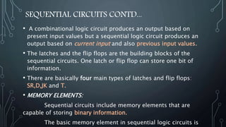
- 3. SEQUENTIAL CIRCUITS CONTD... • A combinational logic circuit produces an output based on present input values but a sequential logic circuit produces an output based on current input and also previous input values. • The latches and the flip flops are the building blocks of the sequential circuits. One latch or flip flop can store one bit of information. • There are basically four main types of latches and flip flops: SR,D,JK and T. • MEMORY ELEMENTS: Sequential circuits include memory elements that are capable of storing binary information. The basic memory element in sequential logic circuits is
- 4. TYPES OF SEQUENTIAL CIRCUITS • There are two main types of sequential circuits.Their classification depends on the timing of their signals. Synchronous sequential circuits Asynchronous sequential circuits Synchronous sequential circuits use level inputs and clock signals as the circuit inputs having limitations on the circuit propagation time and pulse width to generate the output. Asynchronous sequential circuits perform their operation without depending on the clock signals but use the input pulses and generate the output.
- 5. DIFFERENCE BETWEEN LATCHES & FLIP-FLOP LATCHES • Latches do not have a clock signal. • Works with only binary input. • Level triggered • Asynchronous • Operation is faster in latches. FLIP –FLOPS • Flip flop always has a clock signal. • Works with binary input as well as the clock signal. • Edge triggered. • Synchronous • Operation is comparatively slower due to clock signal.
- 6. APPLICATIONS OF SEQUENTIAL CIRCUITS • Shift registers • Flip Flops • Analog to digital and digital to analog converters • Counters • Clocks • Used as registers inside microprocessors and controllers to store temporary information.
- 7. TABLE OF CONTENTS • SR latch (Active high) • SR latch (Active low) • SR Flip-flop(Active high) • SR Flip-flop(Active low) • D Flip-flop • Master slave flip-flop • JK Flip-flop • T Flip-flop THIS INDICATES THAT THE KEY IS IN “ ON” CONDITION . i.e 1 THIS INDICATES THAT THE KEY IS IN “OFF” CONDITION. i.e 0 IMPORTANT POINT:
- 8. SR LATCH ACTIVE HIGH This SR latch is sometimes referred as direct coupled RS flipflop. • In an active high SR Latch two cross coupled NOR gates are used. • When the SET input goes high , the output also goes high.[SET] • When the SET input returns to low , however the output remains High.[HOLD] • The output stays High until the RESET input goes High. MAJOR PROBLEM: In an S-R Latch ,activation of S input sets the circuit, while activation of R input resets the circuit. If both S and R inputs are activated simultaneously , the circuit will be in an invalid condition. KEY POINT: Active high is S based when S and R are contrary to each other.
- 9. ACTIVE HIGH SET ACTIVE HIGH RESET From the truth table , we infer that for SET condition , input of S should be 1 and input of R is 0 then the Q value will be 1 and the LED of Q will glow. From the truth table , we infer that for RESET condition , input of S value is 0 and input of R is 1.Here the complement of Q will be 1 and LED of Q complement glows.
- 10. SR LATCH ACTIVE LOW • In an active low SR Latch two cross coupled NAND gates are used. • When the RESET input goes high , the output Q also goes high.[SET] • When the RESET input returns to low, the output Q also returns to low.[RESET] • When both the inputs are high , then the output Q will remains same.[HOLD] MAJOR PROBLEM: If both S and R inputs are low , then the circuit will be in an invalid condition. KEY POINT: Active low is R based when S and R are contrary to each other.
- 11. ACTIVE LOW SET ACTIVE LOW RESET From the truth table , we infer that for SET condition , input of S is 0 and input of R is 1 then the Q value will be 1 and LED of output Q glows. From the truth table , we infer that for RESET condition , input of S is 1 and input of R is 0 then the Q complement will be 1 and LED of Q complement glows.
- 12. SR FLIP-FLOP • The basic flipflop as it stands is an asynchronous sequential circuit . By addig gates to the inputs of the basic circuit , the flipflop can be made to respond to input levels during the occurrence of a clock pulse. • It consists of: • Two NOR gates and two AND gates along with a clock for ACTIVE HIGH SR • Four NAND gates along with a clock for ACTIVE LOW SR • The inputs are S ,R , and the clock .The outputs are Q and Q complement.
- 13. ACTIVE HIGH SR FLIP-FLOP • The circuit is formed by adding two AND gates to NOR based SR flipflop. • A clock pulse is given as input to both the extra AND gates.
- 14. ACTIVE HIGH SET ACTIVE HIGH RESET For SET condition , input of S should be 0 , input of R is 1 and clock pulse is 1 then the Q value will be 1 and the LED of Q will glow. For RESET condition , input of S value is 1, input of R is 0 and the clock pulse is 1.Here the complement of Q will be 1 and LED of Q complement glows.
- 15. ACTIVE LOW SR FLIP-FLOP • The circuit is formed by adding two NAND gates to NAND based SR flipflop. • A clock pulse is given as input to both the extra NAND gates.
- 16. ACTIVE LOW SET ACTIVE LOW RESET For SET condition , input of S is 1 , input of R is 0 and clock is set to 1 then the Q value will be 1 and LED of output Q glows. For RESET condition , input of S is 0 , input of R is 1 and clock is 1 then the Q complement will be 1 and LED of Q complement glows.
- 17. D FLIP-FLOP • A D flip flop is by far the most important of all the clocked flip-flops. • It is used to create a delay in the circuit. • It is a modification of SR clocked flipflop with the addition of an inverter to prevent S and R inputs from being at the same logic level. • The next state of the flip flop is the same as the D input and is independent of the present state. • if the data input is held HIGH the flip flop would be “SET” and when it is low the flipflop would change and become “RESET”.[Clock is 1 for both the conditions].
- 18. D FLIP-FLOP ACTIVE HIGH • For Active High D flipflop , two AND gates and two NOR gates are being used along with an inverter and a clock. • The D input directly goes to the AND gate(U11) and its complement goes to the other AND gate(U12).
- 19. ACTIVE HIGH 0-I/P ACTIVE HIGH 1-I/P Here the data input is given as 0 and the clock input is 1 .The output value 1 is received at Q and so the LED of Q glows. Here both the clock input and the data input is 1.The output value 1 is received at the Q complement and so the LED of Q complement glows here NOTE: I/P-
- 20. D FLIP-FLOP ACTIVE LOW • For Active Low D Flip-Flop, four NAND gates along with an inverter and a clock is being used. • The first two NAND gates (i.e U2 and U3) form a basic flip flop and gates U8 and U9 modify it into a clocked RS FLIPFLOP. • Here the D input goes to the NAND gate (U8) and its complement to the other NAND gate(U9).
- 21. ACTIVE LOW 0-I/P ACTIVE LOW 1-I/P Here the data input is given as 0 and the clock input is 1 .The output value 1 is received at Q complement and so the LED of Q complement glows. Here the data input is given as 1 and the clock input is 1 .The output value 1 is received at Q and so the LED of Q glows. NOTE: I/P- Input
- 22. MASTER SLAVE FLIP-FLOP • A master slave flipflop is constructed from two separate flipflops. • One circuit serves as a master and the other as a slave. • A clock and an inverter is present in the circuit. • The output from the master flipflop is connected to the two inputs of the slave flipflop. • Each flipflop is connected to a clock pulse complementary to each other. • If the clock pulse is in high state , the master flip flop is in ENABLE state and the slave flipflop is in DISABLE state. • If the clock pulse is in low state , the master flipflop is in DISABLE state and the slave flipflop is ENABLE state. • The types of Master Slave flipflop are listed below: • Master slave SR flipflop • Master slave JK flipflop The above diagram is Master slave SR flipflop.
- 23. JK FLIP-FLOP • A JK flipflop is a refinement of the RS flipflop. • Inputs J and K behave like S and R J-SET and K-CLEAR • It is one of the most useful and versatile flipflop. • The unique features are: If the J and K inputs are both at 1 and the clock pulse is applied , then the output will change state ,regardless of its previous condition. If both J and K inputs are at 0 and the clock pulse is applied there will be no change in the output. There is no indeterminate condition in the operation of JK flipflop.
- 24. JK FLIP-FLOP SET JK FLIP-FLOP RESET Here J input is 1 and K input is 0 and the clock pulse is 1 and so the output 1 is received at Q hence LED of Q glows. Here J is 0 , K is 1 and the clock pulse is also 1.The output 1 is received at Q complement and so LED of Q complement glows.
- 25. JK FLIP-FLOP PGT AND NGT • PGT is Positive Going Transition when clock pulse goes from 0 to 1 • NGT is Negative Going Transition when clock pulse goes from 1 to 0 • NGT is represented using a BUBBLE. • Transitions are also called Edges
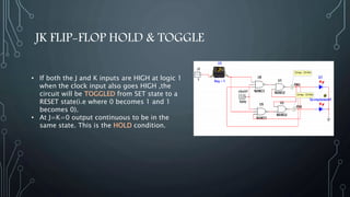
- 26. JK FLIP-FLOP HOLD & TOGGLE • If both the J and K inputs are HIGH at logic 1 when the clock input also goes HIGH ,the circuit will be TOGGLED from SET state to a RESET state(i.e where 0 becomes 1 and 1 becomes 0). • At J=K=0 output continuous to be in the same state. This is the HOLD condition.
- 27. T FLIP-FLOP • The T flipflop is a single input version of JK flipflop. • The T flipflop is obtained from a JK type if both the inputs are tied together. • The designation T comes from the ability of the flipflop to “TOGGLE” . • Regardless of the present state of the flipflop , it assumes the complement state when the clock pulse occurs while input T is logic 1. • T flipflop can be designed from SR ,JK and D flipflop because T flipflop is not available as ICs. • But mostly we use JK flipflop to get T flipflop. • Hence it is also referred as single input JK flipflop and it is considered to be the simplest construction among all other flipflops. • T is TOGGLE INPUT
- 28. SUMMARY:
- 29. 1) C.MURALIDHARAN Assistant Professor , Biomedical Engineering , Rajalakshmi Engineering College 2) A.SUBHA SHREE Student , Biomedical Engineering , Rajalakshmi Engineering College 3) V.A.SAIRAM Student , Biomedical Engineering , Rajalakshmi Engineering College
- 30. THANK YOU