SlideShare a Scribd company logo
UNIT-III
I/O interface with 8255-PPI, 8255-various modes of
operation and interfacing to 8086, interrupt structure
of 8086, serial communication standards, 8251
USART architectures and its interfacing to 8086, RS-
232C. 8257 DMA controller and its interfacing to
8086, memory interfacing to 8086.
1
I/O Interface
INTRO TO I/O INTERFACE
• I/O instructions are IN, INS, OUT, and OUTS
• Also isolated (direct I/O or mapped I/O) and
memory-mapped I/O, the basic input and output
interfaces, and handshaking.
• Knowledge of these topics makes it easier to
understand the connection and operation of the
programmable interface components
and I/O techniques.
The I/O Instructions
• One type of instruction transfers information
to an I/O device (OUT).
• Another reads from an I/O device (IN).
• Instructions are also provided to transfer strings of
data between memory and I/O.
– INS and OUTS, found except the 8086/8088
Input port: Output port:
Personal Computer I/O Map
– the PC uses part of I/O map for
dedicated functions, as shown here
– I/O space between ports 0000H and 03FFH is
normally reserved for the system and ISA bus
(Industry Standard Architecture bus)
– ports at 0400H–FFFFH are generally available
for user applications, main-board functions, and
the PCI bus (Peripheral Controller Interconnect)
PROGRAMMABLE
PERIPHERAL
INTERFACE -8255
Introduction
• It is a programmable device.
• It is an I/O port chip used for interfacing I/O
devices with microprocessor
• Very commonly used peripheral chip
• Knowledge of 8255 essential for students in the
Microprocessors lab for Interfacing experiments
8255 Ports
• 8255 PPI has three 8-bit ports.
• Port A (PA)
• Port B (PB)
• Port C (PC)
• Port C composed of two independent 4-bit ports: PC7-4
(PC Upper) and PC3-0 (PC Lower)
• Port A, Port B, Port C and Control port will have the
addresses as 7CH, 7DH, 7EH, and 7FH respectively.
Block Diagram
Data Bus buffer:
• It is a 8-bit bidirectional Data bus.
• Used to interface between 8255 data bus with
system bus.
• The internal data bus and Outer pins D0-D7 pins
are connected in internally.
• The direction of data buffer is decided by
Read/Control Logic.
Read/Write Control Logic:
• This is getting the input signals from control bus
and Address bus
• Control signal are RD and WR.
• Address signals are A0,A1,and CS.
• 8255 operation is enabled or disabled by CS.
Group A and Group B control:
• Group A and B get the Control Signal from
CPU and send the command to the individual
control blocks.
• Group A send the control signal to port A and
Port C (Upper) PC7-PC4.
• Group B send the control signal to port B and
Port C (Lower) PC3-PC0.
PORT A:
• This is a 8-bit buffered I/O latch.
• It can be programmed by mode 0 , mode 1,
mode 2 .
PORT B:
• This is a 8-bit buffer I/O latch.
• It can be programmed by mode 0 and mode 1.
PORT C:
• This is a 8-bit Unlatched buffer Input and an
Output latch.
• It is spitted into two parts.
• It can be programmed by bit set/reset operation.
Pin Diagram
Pin Description
• PA7-PA0 : These are eight port A lines that acts as either
latched output or buffered input lines
depending upon the control word loaded into the
control word register.
• PC7-PC4 : Upper nibble of port C lines. They may act as
either output latches or input buffers lines.
This port also can be used for generation of
handshake lines in mode 1 or mode 2.
• PC3-PC0 : These are the lower port C lines, other details
are the same as PC7-PC4 lines.
• PB0-PB7 : These are the eight port B lines which are used
as latched output lines or buffered input lines in the
same way as port A.
Pin Description(Contd…)
• RD : This is the input line driven by the
microprocessor and should be low to indicate read
operation to 8255.
• WR : This is an input line driven by the
microprocessor. A low on this line indicates write
operation.
• CS : This is a chip select line. If this line goes low, it
enables the 8255 to respond to RD and WR
signals, otherwise RD and WR signal are
neglected.
• A1-A0: These are the address input lines and are driven
by the microprocessor.
• RESET : The 8255 is placed into its reset state if this
input line is a logical 1. All peripheral ports are set to
8255 Operations
• The lines A1-A0 with RD, WR and CS form the
following operations for 8255.
Programming 8255
• 8255 has three operation modes: mode 0, mode 1,
and mode 2
Mode 0 - Simple Input or Output mode
Mode 1 - Input or Output with Handshake mode
Mode 2 - Bidirectional Data Transfer mode
Mode 0 - Simple Input or Output
• In this mode, ports A, B are used as two simple 8-
bit I/O ports & port C as two independent 4-bit
ports.
• Each port can be programmed to function as simply
an input port or an output port.
• The input/output features in Mode 0 are as follows.
1. Outputs are latched.
2. Inputs are not latched.
3. Ports don’t have handshake or interrupt capability.
• Many I/O devices accept or release information
slower than the microprocessor.
• A method of I/O control called handshaking or
polling, synchronizes the I/O device with the
microprocessor.
• An example is a parallel printer that prints a few
hundred characters per second (CPS).
Handshaking
Mode 1 - Input or Output with Handshake
• In this mode, handshake signals are exchanged
between the MPU and peripherals prior to data
transfer.
• The features of the mode include the following:
1. Two ports (A and B) function as 8-bit I/O ports.
They can be configured as either as input or output ports.
2. Each port uses three lines from port C as handshake
signals.
The remaining two lines of Port C can be used for simple I/O
operations.
3. Input and Output data are latched.
4. Interrupt logic is supported.
Example:
• The computer send the data to the printer large
speed compared to the printer.
• When computer send the data according to the
printer speed at the time only, printer can accept.
• If printer is not ready to accept the data then after
sending the data bus , computer uses another
handshaking signal to tell printer that valid data is
available on the data bus.
• Each port uses three lines from port C as
handshake signals
Mode 1 - Input or Output with Handshake
Mode 2 - Bidirectional Data Transfer
• This mode is used primarily in applications such as
data transfer between two computers.
• In this mode, Port A can be configured as the
bidirectional port, Port B either in Mode 0 or Mode 1.
• Port A uses five signals from Port C as
handshake signals for data transfer.
• The remaining three signals from Port C can be
used either as simple I/O or as handshake for port B.
8255 Modes Summary
• Port A can work in Mode 0, Mode 1, or Mode 2
• Port B can work in Mode 0, or Mode 1
• Port C can work in Mode 0 only, if at all
• Port A, Port B and Port C can work in Mode 0
• Port A and Port B can work in Mode 1
• Only Port A can work in Mode 2
8255 Control Words
• There are 2 control words in 8255.
1. Mode Definition (MD) Control word and
2. Bit Set / Reset (BSR) Control Word
• MD control word configures the ports of 8255 as input or
output in Mode 0, 1, or 2.
• PCBSR control word is used to set to 1 or reset to 0 any one
selected bit of Port C
8255 Control words
1.Mode Definition (MD) Control word
2. Bit Set / Reset (BSR) Control Word
Interfacing with
Advanced Devices
Interrupts
• Definition: The meaning of ‘interrupts’ is to break the
sequence of operation. While the CPU is executing a
program, on ‘interrupt’ breaks the normal sequence of
execution of instructions, diverts its execution to some other
program called Interrupt Service Routine (ISR).After
executing ISR , the control is transferred back again to the
main program. Interrupt processing is an alternative to
polling.
• Need for Interrupt: Interrupts are particularly useful when
interfacing I/O devices that provide or require data at
relatively low data transfer rate.
Different Types of Interrupts
INTERRUPTS
HARDWARE INTERRUPTS SOFTWARE INTERRUPTS
EXTERNAL INTERNAL SYSTEM USER-DEFINED
MASKABLE NON-MASKABLE
DOS INTERRUPTS BIOS INTERRUPTS
Classification 8086 INTERRUPTS
256 INTERRUPTS OF 8086 ARE DIVIDED IN TO 3 GROUPS
1. TYPE 0 TO TYPE 4 INTERRUPTS-
THESE ARE USED FOR FIXED OPERATIONS AND
HENCE ARE CALLED DEDICATED INTERRUPTS
2. TYPE 5 TO TYPE 31 INTERRUPTS
NOT USED BY 8086,RESERVED FOR HIGHER PROCESSORS LIKE
80286 ,80386 ETC
3. TYPE 32 TO 255 INTERRUPTS
AVAILABLE FOR USER,CALLED USER DEFINED INTERRUPTS
THESE CAN BE H/W INTERRUPTS AND ACTIVATED THROUGH
INTR
LINE OR CAN BE S/W INTERRUPTS
TYPE – 0 DIVIDE ERROR INTERRUPT
QUOTIENT IS LARGE CANT BE FIT IN AL/AX OR DIVIDE BY ZERO
TYPE –1 SINGLE STEP INTERRUPT
USED FOR EXECUTING THE PROGRAM IN SINGLE STEP MODE BY
SETTING TRAP FLAG
TO SET TRAP FLAG PUSHF
MOV BP,SP
OR [BP+0],0100H;SET BIT8
POPF
TYPE – 2 NON MASKABLE INTERRUPT
THIS INTERRUPT IS USED FOR EXECUTING ISR OF NMI PIN
(POSITIVE EGDE SIGNAL). NMI CANT BE MASKED BY S/W
TYPE – 3 BREAK POINT INTERRUPT
USED FOR PROVIDING BREAK POINTS IN THE PROGRAM
TYPE – 4 OVER FLOW INTERRUPT
USED TO HANDLE ANY OVERFLOW ERROR AFTER SIGNED ARITHMETIC
PRIORITY OF INTERRUPTS
INTERRUPT TYPE PRIORITY
INT0,INT3-INT 255,INTO
HIGHEST
NMI(INT2)
INTR
SINGLE STEP
LOWEST
Interrupt Vector Table – IVT (in memory)
• x86 has 256 interrupts, specified by Type Number or Vector
• 1 byte of data must accompany each interrupt; specifies Type
Vector is a pointer (address) into Interrupt Vector Table, IVT
– IVT is stored in memory from 0000:0000 to 0000:03ffh
• IVT contains 256 far pointer values (addresses)
– Far pointer is CS:IP values
• Each far pointer is address of Interrupt Service Routine, ISR
– Also referred to as Interrupt Handler
IVT Format
Offset
Offset
Offset
Segment
Segment
Segment
Interrupt 0
Interrupt 1
Interrupt 255
0000:0000
0000:0001
0000:0002
0000:0003
0000:0004
0000:0005
0000:0006
0000:0007
0000:03fc
0000:03fd
0000:03fe
0000:03ff
IP LSB
IP MSB
CS LSB
CS MSB
Given a Vector, where is the
ISR address stored in memory ?
4
Offset Type
 
Example: int 36h
Offset = (544) = 216
= 00d8h
Structure of Interrupt Vector Table 8086/88
Interrupt Service Routine (ISR)
• Similar to a subroutine
• Attends to the request of an interrupting source
– Clears the interrupt flag
– Should save register contents that may be affected by
the code in the ISR
– Must be terminated with the instruction RETFIE
• When an interrupt occurs, the MPU:
– Completes the instruction being executed
– Disables global interrupt enable
– Places the return address on the stack
Interrupt Service Routine (ISR)
• High-priority interrupts
– The contents of W, STATUS, and BSR registers are
automatically saved into respective shadow registers.
• Low-priority interrupts
– These registers must be saved as a part of the ISR
• If they are affected
• RETFIE [s] ;Return from interrupt
• RETFIE FAST ;FAST equivalent to s = 1
– If s =1: MPU also retrieves the contents of W,
BSR, and
STATUS registers
DOS & BIOS Introduction
•INT10 Video services
•INT13 Disk Services
•INT16 Keyboard functions
•INT17 Parallel printer functions
BIOS
functions
(Basic
Input/
Output
System)
DOS
functions
(Disk
Operating
System)
•INT21
•keyboard
•display
•printer
•disk
•date/time
•memory management
•program control
Reserved
INTs
DOS INT 21, function 01H: Wait for Keyboard Input
Specification: waits for the user to press a key on the keyboard and
returns the ASCII code.
Input: AH = 01 (function code)
Output: AL = ASCII code of the pressed key. The character is echoed to
the video display
Constrain: doesn’t return the control to the main program until a key is
pressed.
If the key correspond to an extended ASCII code, AL returns 00. The next
INT 21, function 01 returns in AL the extended ASCII code.
DOS INT 21, function 08H: Console Input without Echo
Specification: similar to function 01 but no echo on video display.
DOS Functions-Using the Keyboard
Ex:
MOV ah, 01H; Request keyboard input
INT 21h
DOS INT 21, function 02H: Display Output
Specification: writes a single character to the display screen, at the current
cursor position.
Input: AH = 02 (function code), DL = ASCII character to be sent to display.
Control characters perform their specific action (0DH = Carriage Return,
0AH = Line Feed, 08H = Backspace, etc.).
DOS INT 21, function 09H: Display A CHARACTER String
Specification: Send to display a string in the current data segment. The
string ends with ’$’ character (not displayed).
Input: AH = 09 (function code), DX = The offset of the first character in the
string.
Controlling the Video Display
Ex:
String DB “Enter your name: $”
MOV AH, 09h; request display
LEA DX, String; load address
INT 21h
Ex: MOV AH, 02h;request character display
MOV DL, ‘S’
INT 21h
BIOS INT 16, function 00H: Read keyboard Input
Specification: similar to INT21 function 01 but if the pressed key
correspond to an extended ASCII code, AL returns 00 and AH returns the
extended ASCII code. No echo to display.
BIOS INT 16, function 01H: Read keyboard status
Specification: doesn’t wait. If the keyboard buffer is empty, ZF is set to 1. If
not, returns the first ASCII code from buffer in the same way like function 00,
and clear ZF.
BIOS Functions: Using the Keyboard
BIOS INT 16, function 02H: Return Shift Flag Status
Specification: waits for the user to press a key on the keyboard and
returns the ASCII code.
Input: AH = 02 (function code)
Output: AL = Status of the special function keys:
B7=Insert, B6=Caps Lock, B5=Num Lock, B4=Scroll Lock (active bit=1
=> function active)
B3=Alt, B2=Ctrl, B1=Left Shift, B0=Right Shift (active bit=1 => button
pressed )
Using the Keyboard(Contd…)
BIOS INT 10, function 00H: Set Video Mode
Specification: set video mode of the display (ex: mode 1 = 25
linesX40 characters,
mode 3 = 25 linesX80 characters).
Input: AH = 00 (function code), AL = The desired video mode .
BIOS INT 10, function 0FH: Read Current Video Mode
Specification: returns video mode of the display.
Input: AH = 0F (function code)
Output: AL = The current video mode.
Controlling the Video Display(Contd…)
BIOS INT 10, function 02H: Set Cursor Position
Specification: moves the cursor to specified position (in text mode).
Input: AH = 02 (function code), DH = the row (0-24), DL column (0-79), BH
= page (0)
BIOS INT 10, function 03H: Read the Current Cursor Position
Input: AH = 02 (function code), BH = page (0)
Output: DH = the row (0-24), DL column (0-79)
Controlling the Video Display(Contd…)
BIOS INT 10, function 0AH: Write Character to Screen
Specification: write multiple times a character to screen at current cursor
position.
Input: AH = 0A (function code), AL = ASCII code, BH = page number, CX =
repeat value.
BIOS INT 10, function 09H: Write Character/Attribute to
Screen
Specification: write multiple times a character to screen at current cursor
position. Specify the video attribute of the character: B7 = blink, (B6 = red, B5
= green, B4 = blue)=background, B3 = intensity, (B2 = red, B1 = green, B0 =
blue)=foreground
Input: AH = 09 (function code), AL = ASCII code, BH = page number,
BL = character’s attribute, CX = repeat value.
Controlling the Video Display(Contd…)
BIOS INT 10, function 08H: Read Character/Attribute from
Screen
Input: AH = 08 (function code), BH = display page (0)
Output: AL = The Character code at the current cursor position, AH = the
attribute byte.
BIOS INT 10, function 06H: Scroll Current Page Up
Input: AH = 06 (function code)
AL = Number of rows to scroll up (0 for entire region)
BH = attribute for scrolled region
CH = Row number at top of region
CL = Column number at left of the region
DH = Row number at bottom of region
DL = Column number at right of the region
Controlling the Video Display(Contd…)
Examples: in the textbook!
Unit-3 IO Interfacing-1.pptximportant questions to be noted
Serial Vs Parallel Data Transfer
Synchronous Vs Asynchronous
• Asynchronous transfer does not require clock signal.
• However, it transfers extra bits(start bits and stop bits) during data
communication.
• Synchronous does not transfer extra bits. However, it requires
clock signal.
Synchronous Data Communication
Asynchronous Data Communication
8251 USART
• The 8251 USART (Universal Synchronous Asynchronous
Receiver Transmitter) is capable of implementing either
an asynchronous or synchronous serial data
communication.
• As a peripheral device of a microcomputer system, the
8251 receives parallel data from the CPU and transmits
serial data after conversion.
• This device also receives serial data from the outside and
transmits parallel data to the CPU after conversion.
8251 Pin Diagram
8251 Block Diagram
Pin Description
• D0 - D7 - This is bidirectional data bus which receive control words
and transmits data from the CPU and sends status words and
received data to CPU.
• RESET - A "High" on this input forces the 8251 into "reset status”.
The min. reset width is six clock inputs during the operating status
of CLK.
• CLK - CLK signal is used to generate internal device timing. CLK
signal is independent of RXC or TXC.
• WR - This is the "active low" input terminal which receives a signal
for writing transmit data and control words from the CPU into the
8251.
Pin Description
• RD - This is the "active low" input terminal which receives a signal
for reading receive data and status words from the 8251.
• C/D - This is an input terminal which receives a signal for selecting
data or command words and status words when the 8251 is
accessed by the CPU.
• CS - This is the "active low" input terminal which selects the 8251 at
low level when the CPU accesses.
Pin Description
• TXD - This is an output terminal for transmitting data from which
serial-converted data is sent out.
• TXRDY - This is an output terminal which indicates that the 8251 is
ready to accept a transmitted data character.
• TXEMPTY - This is an output terminal which indicates that the 8251
has transmitted all the characters and had no data character.
• TXC - This is a clock input signal (Active Low) which determines the
transfer speed of transmitted data.
– In "synchronous mode," the baud rate will be the same as the frequency of
TXC. In "asynchronous mode", it is possible to select the baud rate factor by
mode instruction. It can be 1, 1/16 or 1/64 the TXC.
Pin Description
• RXD - This is a terminal which receives serial data.
• RXRDY - This is a terminal which indicates that the 8251 contains a
character that is ready to READ.
– If the CPU reads a data character, RXRDY will be reset by the leading edge of
RD signal. Unless the CPU reads a data character before the next one is
received completely, the preceding data will be lost. In such a case, an
overrun error flag status word will be set.
• RXC - This is a clock input signal which determines the transfer
speed of received data.
– In "synchronous mode," the baud rate is the same as the frequency of RXC. In
"asynchronous mode," it is possible to select the baud rate factor by mode
instruction. It can be 1, 1/16, 1/64 the RXC.
Pin Description
• SYNDET/BD - This is a terminal whose function changes according to
mode.
– In “internal synchronous mode“, this terminal is at high level, if sync
characters are received and synchronized.
– If a status word is read, the terminal will be reset.
– In “external synchronous mode”, this is an input terminal. A "High" on
this input forces the 8251 to start receiving data characters.
– In “asynchronous mode”, this is an output terminal which generates
"high level“ output upon the detection of a "break" character if
receiver data contains a "low-level" space between the stop bits of two
continuous characters.
– The terminal will be reset, if RXD is at high level. After Reset is active,
the terminal will be output at low level.
Pin Description
• DSR - This is an input port for MODEM interface. The input status of
the terminal can be recognized by the CPU reading status words.
• DTR - This is an output port for MODEM interface. It is possible to
set the status of DTR by a command.
• CTS - This is an input terminal for MODEM interface which is used
for controlling a transmit circuit.
– The terminal controls data transmission if the device is set in "TX Enable"
status by a command. Data is transmittable if the terminal is at low level.
• RTS - This is an output port for MODEM interface. It is possible to
set the status RTS by a command.
8251 functional configuration
• The 8251 functional configuration is programmed by software.
• Operation between the 8251 and a CPU is executed by program
control.
• Table 1 shows the operation between a CPU and the device.
Simple Serial I/O Procedures
8251 Control Words
• There are two types of control word.
1. Mode instruction (setting of function)
2. Command (setting of operation)
• Apart from the control words, a Status Word is present in
8251 to see the internal status.
1. Mode instruction word
• Mode instruction is used for setting the function of the 8251.
• Mode instruction will be in "wait for write" at either internal reset
or external reset.
• That is, the writing of a control word after resetting will be
recognized as a "mode instruction.“
• Items set by mode instruction are as follows:
– Synchronous/asynchronous mode
– Stop bit length (asynchronous mode)
– Character length
– Parity bit
– Baud rate factor (asynchronous mode)
– Internal/external synchronization (synchronous mode)
– Number of synchronous characters (Synchronous mode)
Mode Instruction - Asynchronous
Mode Instruction - Synchronous
2. Command Word
• Command is used for setting the operation of the 8251.
• It is possible to write a command whenever necessary
after writing a mode instruction and sync characters.
• Items to be set by command are as follows:
– Transmit Enable/Disable
– Receive Enable/Disable
– DTR, RTS Output of data.
– Resetting of error flag.
– Sending to break characters
– Internal resetting
– Hunt mode (synchronous mode)
Bit
Configurable
Command
Word Format
Status Word Format
RS232
• RS-232 (Recommended standard-232) is a standard
interface approved by the Electronic Industries
Association (EIA) for connecting serial devices.
• In other words, RS-232 is a long established standard
that describes the physical interface and protocol for
relatively low-speed serial data communication between
computers and related devices.
Limitations of RS-232
 Firstly, the interface presupposes a common ground between the DTE and DCE.
 Secondly, a signal on a single line is impossible to screen effectively for noise
 Low capacitance cable can reduce crosstalk.
 Higher frequency that are the problem, control of slew rate in the signal (i.e.,
making the signal more rounded, rather than square) also decreases the
crosstalk.
 Voltage levels with respect to ground represent the RS 232 signals.
 Interface is useful for point-to-point communication at slow speeds.
 Port COM1 in a PC can be used for a mouse, port COM2 for a modem, etc.
 Implies limited cable length - about 30 to 60 meters maximum. (Main problems
are interference and resistance of the cable.)
 Shortly, RS 232 was designed for communication of local devices, and supports
one transmitter and one receiver.
Unit-3 IO Interfacing-1.pptximportant questions to be noted
Direct memory access
• Direct memory access (DMA) is a process in which
an external device takes over the control of system
bus from the CPU.
• DMA is for high-speed data transfer from/to mass
storage peripherals, e.g. hard disk drive, magnetic
tape, CD-ROM, and sometimes video controllers.
• The basic idea of DMA is to transfer blocks of data
directly between memory and peripherals.
• The data don’t go through the microprocessor but
the data bus is occupied.
Basic process of DMA – Minimum Mode
• The HOLD and HLDA pins are used to receive and
acknowledge the hold request respectively.
• Normally the CPU has full control of the system bus.
• In a DMA operation, the peripheral takes over bus control
temporarily.
Basic process of DMA – Maximum Mode
• The RQ/GT1 and RQ/GT0 pins are used to issue
DMA request and receive acknowledge signals.
• Sequence of events of a typical DMA process:
1. Peripheral asserts one of the request pins, e.g. RQ/GT1
or RQ/GT0 (RQ/GT0 has higher priority)
2. 8086 completes its current bus cycle and enters into a
HOLD state.
3. 8086 grants the right of bus control by asserting a grant
signal via the same pin as the request signal.
4. DMA operation starts.
5. Upon completion of the DMA operation, the peripheral
asserts the request/grant pin again to relinquish bus
control.
DMA controller
• A DMA controller interfaces with several peripherals that
may request DMA.
• The controller decides the priority of simultaneous DMA
requests communicates with the peripheral and the CPU,
and provides memory addresses for data transfer.
• DMA controller commonly used with 8086 is the
8257/8237 programmable device.
• The 8257/8237 is a 4-channel device.
• Each channel is dedicated to a specific peripheral
device and capable of addressing 64 K bytes section of
memory.
8237 - DMA Controller
Unit-3 IO Interfacing-1.pptximportant questions to be noted
8237 Registers
1. Current address register
2. Current word register
3. Command register
4. Mode register
5. Request register
6. Mask register
7. Status register
8. Temporary register
8237 Registers
1.Current address register
• One 16-bit register for each channel
• Holds address for the current DMA transfer
2.Current word register
• Keeps the byte count
• Generates terminal count (TC) signal when the count
goes from zero to FFFFH
3.Command register
• Used to program 8257
8237 Registers
4.Mode register
• Each channel can be programmed to
– Read or write
– Autoincrement or autodecrement the address
– Autoinitialize the channel
5.Request register
• For software-initiated DMA
6.Mask register
• Used to disable a specific channel
7.Status register
8.Temporary register
• Used for memory-to-memory transfers
Keyboard Interface
• In most keyboards, the key switches are connected
in a matrix of Rows and Columns.
• Getting meaningful data from a keyboard requires
three major tasks:
1. Detect a key press
2. Debounce the key press.
3. Encode the key press (produce a standard code
for the pressed key).
• Logic ‘0’ is read by the microprocessor when the
key is pressed.
Keyboard Interface(Contd…)
Key Debounce:
Whenever a mechanical push-bottom is pressed or
released once, the mechanical components of the
key do not change the position smoothly; rather it
generates a transient response. These may be
interpreted as the multiple pressures and responded
accordingly.
Keyboard Interface(Contd…)
– the 82C55 is decoded at I/O ports 50H–53H for
an 8086
– port A is programmed as an input port to read the
rows
– port B is programmed as an output port to select
a column
– a flowchart of the software required to read a key
from the keyboard matrix and debounce the key
is illustrated in Fig.
Keyboard Interface(Contd…)
Flow Chart
Keyboard Interface(Contd…)
– keys must be debounced, normally with a time delay of
10–20 ms
– the software uses a procedure called SCAN to scan the
keys and another called DELAY10 to waste 10 ms of time
for debouncing
– the main keyboard procedure is called KEY and appears
in Example.
– the KEY procedure is generic, and can handle any
configuration from a 1  1 matrix to an 8  8 matrix.
8 Digit LED Display
7 segment display
a
b
c
g
d
e
f
Digit-abcdefg-hex
0-1111110-7E 1-0110000-30
2-1101101-6D 3-1111001-79
4-0110011-33 5-1011011-5B
6-1011111-5F 7-1110000-70
8-1111111-7F 9-1111011-7B
A-1110111-77 B-0011111-1F
C-1001110-4E D-0111101-3D
E-1001111-4F F-1000111-47
Stepper Motor Interface
Fig.1 Internal schematic of a four
winding stepper motor
Fig.2 Winding arrangement of a stepper
motor.
Contd…
Stepper Motor Interface
•A simple scheme for rotating the shaft of a stepper motor
is called a wave scheme
•In this scheme, windings Wa,Wb, Wc and Wd are applied
with the required voltage pulses, in a cyclic fashion.
•By reversing the sequence of excitation, the direction of
rotation of the stepper motor shaft may be reversed. Table
below shows the excitation sequences for clockwise and
anticlockwise rotations.
Example:
•Design a stepper motor controller and write an ALP to
rotate shaft of a 4-phase stepper motor
•(i) in clockwise 5 rotations
•(ii) in anticlockwise 5 rotations
•The 8255 port A address is 0740h. The stepper has 200
rotor teeth
•The port A bit PA0 drives winding Wa, PA1 drives Wb and so
on.
•The stepper motor has an initial delay of 10 msec. Assume
that the routine for this delay is already available
Assembly Code
For anticlockwise direction
Clockwise:
MOV DX,0FFE6
MOV AL,80
OUT DX,AL
MOV CX,0FFFF
MOV DX,OFFE0
MOV AL,11
X:OUT DX,AL
CALL DELAY
ROR AL,1
LOOP X
DELAY:MOV BX,0FFF
Y:DEC BX
JNZ Y
RET
ANTICLOCKWISE:
MOV DX,0FFE6
MOV AL,80
OUT DX,AL
MOV CX,0FFFF
MOV DX,OFFE0
MOV AL,11
X:OUT DX,AL
CALL DELAY
ROL AL,1
LOOP X
DELAY:MOV BX,0FFF
Y:DEC BX
JNZ Y
RET
Interfacing Analog to Digital Data Converters
General algorithm for ADC interfacing contains the following
steps:
• Ensure the stability of analog input, applied to the ADC.
• Issue start of conversion pulse to ADC
• Read end of conversion signal to mark the end of conversion
processes.
• Read digital data output of the ADC as equivalent digital
output.
• Analog input voltage must be constant at the input of the ADC
right from the start of conversion till the end of the conversion
to get correct results. This may be ensured by a sample and
hold circuit which samples the analog signal and holds it
constant for specific time duration. The microprocessor may
issue a hold signal to the sample and hold circuit.
• If the applied input changes before the complete conversion
process is over, the digital equivalent of the analog input
calculated by the ADC may not be correct.
Interfacing Analog to Digital Data Converters
Fig.1 Block Diagram of ADC 0808/0809
Contd…
Interfacing Analog to Digital Data Converters
Fig.2 Pin Diagram of ADC 0808/0809
Fig.3 Timing Diagram Of ADC 0808.
Contd…
Interfacing Analog to Digital Data Converters
Fig: Interfacing ADC0808 with 8086
Contd…
Interfacing Digital To Analog Converters
Pin Diagram of DAC 0800
Contd…
Interfacing Digital To Analog Converters
Fig:Interfacing DAC0800 with 8086
Square Wave
A 3000 // (starting address)
MOV AL,80
MOV DX,0FFE6
OUT DX,AL
MOV DX,0FFE0
XX: MOV AL,00
OUT DX,AL
CALL 5000 //(delay address) MOV
DX,0FFE0
MOV AL,0FF
OUT DX,AL
CALL 5000 // (delay address) JMP
XX
INT 03
DELAY PROGRAM
A 5000 //( delay address)
MOV CX,00FF
YY: LOOP
YY RET
Triangle Wave
A 3000 //(starting address)
MOV AL,80
MOV DX,0FFE6
OUT DX,AL
XX:MOV AL,0FF
YY:MOV DX,0FFE0
OUT DX,AL
MOV DX,0FFE2
OUT DX,AL
DEC AL
JNZ YY
ZZ:MOV DX,0FFE2
OUT DX,AL
MOV DX,0FFE0
OUT DX,AL
INC AL
CMP AL,0FF
JNZ ZZ
JMP XX
INT 03
Memory Interfacing
Design an 8086 based system with the following specifications with
each chip of 32kb i) 64kb EPROM II) 64kb Ram. Draw the complete
schematic of the design indicating address map.
A) 32Kb requires-16 address lines
Unit-3 IO Interfacing-1.pptximportant questions to be noted
2) Design an 8086 based system with the following specifications i) 8
Kb EPROM ii) 8KB Ram Draw the complete schematic of the design
indicating address map.
A) 8Kb requires 13 address lines
Unit-3 IO Interfacing-1.pptximportant questions to be noted
Thank You

More Related Content

Similar to Unit-3 IO Interfacing-1.pptximportant questions to be noted (20)

PPTX
8255_Ppi new
Monica Gunjal
 
PPTX
MPMC UNIT 3 MPMC UNIT 3 MPMC UNIT 3 MPMC UNIT 3
AnbazhaganSelvanatha
 
PPTX
MPMC UNIT 3 MPMC UNIT 3 MPMC UNIT 3 MPMC UNIT 3
AnbazhaganSelvanatha
 
PPTX
8255 ppi.pptx
zahid235639
 
PDF
Unit 3 mpmc
tamilnesaner
 
PPTX
8086 microprocessor -Input/Output INTERFACING
C.Helen Sulochana
 
PDF
8255.pdf
someshdash1
 
PPT
KTU_8255_Programmable Peripheral Interface
roshi4781
 
PDF
8255 & IO Interfacing.pdf
Ilavarasan Tamizh
 
PDF
Unit 3-PROGRAMMABLE PERIPERAL INTERFACE.pdf- MECHATRONICS-ENGGINERING
Chandra Kumar S
 
PPT
MECHATRONICS-Unit 3-PROGRAMMABLE PERIPERAL INTERFACE.ppt
CHANDRA KUMAR S
 
PPTX
8255 Programmble Peripheral Interface
Amit Kumer Podder
 
PPTX
1.ppi 8255
MdFazleRabbi18
 
PPTX
Unit-IV.pptx
ssuser47c811
 
PDF
unit-3-8255.pdf
ShanmukhSaiR
 
PPT
PPI-MECHATRONICS
selvakumar948
 
PPTX
Programmable peripheral interface 8255
Marajulislam3
 
PPTX
Mod-2 M&M.pptx
TechCook1
 
PPT
Programmableperipheralinterface 8255 ppt
sharan Kumar
 
PPT
UNIT III PROGRAMMABLE PERIPHERAL INTERFACE
ravis205084
 
8255_Ppi new
Monica Gunjal
 
MPMC UNIT 3 MPMC UNIT 3 MPMC UNIT 3 MPMC UNIT 3
AnbazhaganSelvanatha
 
MPMC UNIT 3 MPMC UNIT 3 MPMC UNIT 3 MPMC UNIT 3
AnbazhaganSelvanatha
 
8255 ppi.pptx
zahid235639
 
Unit 3 mpmc
tamilnesaner
 
8086 microprocessor -Input/Output INTERFACING
C.Helen Sulochana
 
8255.pdf
someshdash1
 
KTU_8255_Programmable Peripheral Interface
roshi4781
 
8255 & IO Interfacing.pdf
Ilavarasan Tamizh
 
Unit 3-PROGRAMMABLE PERIPERAL INTERFACE.pdf- MECHATRONICS-ENGGINERING
Chandra Kumar S
 
MECHATRONICS-Unit 3-PROGRAMMABLE PERIPERAL INTERFACE.ppt
CHANDRA KUMAR S
 
8255 Programmble Peripheral Interface
Amit Kumer Podder
 
1.ppi 8255
MdFazleRabbi18
 
Unit-IV.pptx
ssuser47c811
 
unit-3-8255.pdf
ShanmukhSaiR
 
PPI-MECHATRONICS
selvakumar948
 
Programmable peripheral interface 8255
Marajulislam3
 
Mod-2 M&M.pptx
TechCook1
 
Programmableperipheralinterface 8255 ppt
sharan Kumar
 
UNIT III PROGRAMMABLE PERIPHERAL INTERFACE
ravis205084
 

Recently uploaded (20)

PDF
The X-Press God-WPS Office.pdf hdhdhdhdhd
ramifatoh4
 
PPT
Lecture 2-1.ppt at a higher learning institution such as the university of Za...
rachealhantukumane52
 
PPTX
things that used in cleaning of the things
drkaran1421
 
PPTX
materials that are required to used.pptx
drkaran1421
 
PPTX
Spark with anjbnn hfkkjn hbkjbu h jhbk.pptx
nreddyjanga
 
PPTX
Pre-Interrogation_Assessment_Presentation.pptx
anjukumari94314
 
PDF
Introduction to Data Science_Washington_
StarToon1
 
PDF
Incident Response and Digital Forensics Certificate
VICTOR MAESTRE RAMIREZ
 
PDF
apidays Munich 2025 - Let’s build, debug and test a magic MCP server in Postm...
apidays
 
PPTX
Enterprise Architecture and TOGAF Presn
starksolutionsindia
 
PPTX
Lecture_9_EPROM_Flash univeristy lecture fall 2022
ssuser5047c5
 
PPTX
This PowerPoint presentation titled "Data Visualization: Turning Data into In...
HemaDivyaKantamaneni
 
PPTX
apidays Munich 2025 - Effectively incorporating API Security into the overall...
apidays
 
PPTX
SRIJAN_Projecttttt_Report_Cover_PPT.pptx
SakshiLodhi9
 
PPTX
recruitment Presentation.pptxhdhshhshshhehh
devraj40467
 
PPTX
Green Vintage Notebook Science Subject for Middle School Climate and Weather ...
RiddhimaVarshney1
 
DOCX
AI/ML Applications in Financial domain projects
Rituparna De
 
PPT
Data base management system Transactions.ppt
gandhamcharan2006
 
PPTX
Introduction to Artificial Intelligence.pptx
StarToon1
 
PPTX
DATA-COLLECTION METHODS, TYPES AND SOURCES
biggdaad011
 
The X-Press God-WPS Office.pdf hdhdhdhdhd
ramifatoh4
 
Lecture 2-1.ppt at a higher learning institution such as the university of Za...
rachealhantukumane52
 
things that used in cleaning of the things
drkaran1421
 
materials that are required to used.pptx
drkaran1421
 
Spark with anjbnn hfkkjn hbkjbu h jhbk.pptx
nreddyjanga
 
Pre-Interrogation_Assessment_Presentation.pptx
anjukumari94314
 
Introduction to Data Science_Washington_
StarToon1
 
Incident Response and Digital Forensics Certificate
VICTOR MAESTRE RAMIREZ
 
apidays Munich 2025 - Let’s build, debug and test a magic MCP server in Postm...
apidays
 
Enterprise Architecture and TOGAF Presn
starksolutionsindia
 
Lecture_9_EPROM_Flash univeristy lecture fall 2022
ssuser5047c5
 
This PowerPoint presentation titled "Data Visualization: Turning Data into In...
HemaDivyaKantamaneni
 
apidays Munich 2025 - Effectively incorporating API Security into the overall...
apidays
 
SRIJAN_Projecttttt_Report_Cover_PPT.pptx
SakshiLodhi9
 
recruitment Presentation.pptxhdhshhshshhehh
devraj40467
 
Green Vintage Notebook Science Subject for Middle School Climate and Weather ...
RiddhimaVarshney1
 
AI/ML Applications in Financial domain projects
Rituparna De
 
Data base management system Transactions.ppt
gandhamcharan2006
 
Introduction to Artificial Intelligence.pptx
StarToon1
 
DATA-COLLECTION METHODS, TYPES AND SOURCES
biggdaad011
 
Ad

Unit-3 IO Interfacing-1.pptximportant questions to be noted

  • 1. UNIT-III I/O interface with 8255-PPI, 8255-various modes of operation and interfacing to 8086, interrupt structure of 8086, serial communication standards, 8251 USART architectures and its interfacing to 8086, RS- 232C. 8257 DMA controller and its interfacing to 8086, memory interfacing to 8086. 1
  • 3. INTRO TO I/O INTERFACE • I/O instructions are IN, INS, OUT, and OUTS • Also isolated (direct I/O or mapped I/O) and memory-mapped I/O, the basic input and output interfaces, and handshaking. • Knowledge of these topics makes it easier to understand the connection and operation of the programmable interface components and I/O techniques.
  • 4. The I/O Instructions • One type of instruction transfers information to an I/O device (OUT). • Another reads from an I/O device (IN). • Instructions are also provided to transfer strings of data between memory and I/O. – INS and OUTS, found except the 8086/8088
  • 6. Personal Computer I/O Map – the PC uses part of I/O map for dedicated functions, as shown here – I/O space between ports 0000H and 03FFH is normally reserved for the system and ISA bus (Industry Standard Architecture bus) – ports at 0400H–FFFFH are generally available for user applications, main-board functions, and the PCI bus (Peripheral Controller Interconnect)
  • 8. Introduction • It is a programmable device. • It is an I/O port chip used for interfacing I/O devices with microprocessor • Very commonly used peripheral chip • Knowledge of 8255 essential for students in the Microprocessors lab for Interfacing experiments
  • 9. 8255 Ports • 8255 PPI has three 8-bit ports. • Port A (PA) • Port B (PB) • Port C (PC) • Port C composed of two independent 4-bit ports: PC7-4 (PC Upper) and PC3-0 (PC Lower) • Port A, Port B, Port C and Control port will have the addresses as 7CH, 7DH, 7EH, and 7FH respectively.
  • 11. Data Bus buffer: • It is a 8-bit bidirectional Data bus. • Used to interface between 8255 data bus with system bus. • The internal data bus and Outer pins D0-D7 pins are connected in internally. • The direction of data buffer is decided by Read/Control Logic.
  • 12. Read/Write Control Logic: • This is getting the input signals from control bus and Address bus • Control signal are RD and WR. • Address signals are A0,A1,and CS. • 8255 operation is enabled or disabled by CS.
  • 13. Group A and Group B control: • Group A and B get the Control Signal from CPU and send the command to the individual control blocks. • Group A send the control signal to port A and Port C (Upper) PC7-PC4. • Group B send the control signal to port B and Port C (Lower) PC3-PC0. PORT A: • This is a 8-bit buffered I/O latch. • It can be programmed by mode 0 , mode 1, mode 2 .
  • 14. PORT B: • This is a 8-bit buffer I/O latch. • It can be programmed by mode 0 and mode 1. PORT C: • This is a 8-bit Unlatched buffer Input and an Output latch. • It is spitted into two parts. • It can be programmed by bit set/reset operation.
  • 16. Pin Description • PA7-PA0 : These are eight port A lines that acts as either latched output or buffered input lines depending upon the control word loaded into the control word register. • PC7-PC4 : Upper nibble of port C lines. They may act as either output latches or input buffers lines. This port also can be used for generation of handshake lines in mode 1 or mode 2. • PC3-PC0 : These are the lower port C lines, other details are the same as PC7-PC4 lines. • PB0-PB7 : These are the eight port B lines which are used as latched output lines or buffered input lines in the same way as port A.
  • 17. Pin Description(Contd…) • RD : This is the input line driven by the microprocessor and should be low to indicate read operation to 8255. • WR : This is an input line driven by the microprocessor. A low on this line indicates write operation. • CS : This is a chip select line. If this line goes low, it enables the 8255 to respond to RD and WR signals, otherwise RD and WR signal are neglected. • A1-A0: These are the address input lines and are driven by the microprocessor. • RESET : The 8255 is placed into its reset state if this input line is a logical 1. All peripheral ports are set to
  • 18. 8255 Operations • The lines A1-A0 with RD, WR and CS form the following operations for 8255.
  • 19. Programming 8255 • 8255 has three operation modes: mode 0, mode 1, and mode 2 Mode 0 - Simple Input or Output mode Mode 1 - Input or Output with Handshake mode Mode 2 - Bidirectional Data Transfer mode
  • 20. Mode 0 - Simple Input or Output • In this mode, ports A, B are used as two simple 8- bit I/O ports & port C as two independent 4-bit ports. • Each port can be programmed to function as simply an input port or an output port. • The input/output features in Mode 0 are as follows. 1. Outputs are latched. 2. Inputs are not latched. 3. Ports don’t have handshake or interrupt capability.
  • 21. • Many I/O devices accept or release information slower than the microprocessor. • A method of I/O control called handshaking or polling, synchronizes the I/O device with the microprocessor. • An example is a parallel printer that prints a few hundred characters per second (CPS). Handshaking
  • 22. Mode 1 - Input or Output with Handshake • In this mode, handshake signals are exchanged between the MPU and peripherals prior to data transfer. • The features of the mode include the following: 1. Two ports (A and B) function as 8-bit I/O ports. They can be configured as either as input or output ports. 2. Each port uses three lines from port C as handshake signals. The remaining two lines of Port C can be used for simple I/O operations. 3. Input and Output data are latched. 4. Interrupt logic is supported.
  • 23. Example: • The computer send the data to the printer large speed compared to the printer. • When computer send the data according to the printer speed at the time only, printer can accept. • If printer is not ready to accept the data then after sending the data bus , computer uses another handshaking signal to tell printer that valid data is available on the data bus. • Each port uses three lines from port C as handshake signals
  • 24. Mode 1 - Input or Output with Handshake
  • 25. Mode 2 - Bidirectional Data Transfer • This mode is used primarily in applications such as data transfer between two computers. • In this mode, Port A can be configured as the bidirectional port, Port B either in Mode 0 or Mode 1. • Port A uses five signals from Port C as handshake signals for data transfer. • The remaining three signals from Port C can be used either as simple I/O or as handshake for port B.
  • 26. 8255 Modes Summary • Port A can work in Mode 0, Mode 1, or Mode 2 • Port B can work in Mode 0, or Mode 1 • Port C can work in Mode 0 only, if at all • Port A, Port B and Port C can work in Mode 0 • Port A and Port B can work in Mode 1 • Only Port A can work in Mode 2
  • 27. 8255 Control Words • There are 2 control words in 8255. 1. Mode Definition (MD) Control word and 2. Bit Set / Reset (BSR) Control Word • MD control word configures the ports of 8255 as input or output in Mode 0, 1, or 2. • PCBSR control word is used to set to 1 or reset to 0 any one selected bit of Port C
  • 28. 8255 Control words 1.Mode Definition (MD) Control word 2. Bit Set / Reset (BSR) Control Word
  • 30. Interrupts • Definition: The meaning of ‘interrupts’ is to break the sequence of operation. While the CPU is executing a program, on ‘interrupt’ breaks the normal sequence of execution of instructions, diverts its execution to some other program called Interrupt Service Routine (ISR).After executing ISR , the control is transferred back again to the main program. Interrupt processing is an alternative to polling. • Need for Interrupt: Interrupts are particularly useful when interfacing I/O devices that provide or require data at relatively low data transfer rate.
  • 31. Different Types of Interrupts INTERRUPTS HARDWARE INTERRUPTS SOFTWARE INTERRUPTS EXTERNAL INTERNAL SYSTEM USER-DEFINED MASKABLE NON-MASKABLE DOS INTERRUPTS BIOS INTERRUPTS
  • 32. Classification 8086 INTERRUPTS 256 INTERRUPTS OF 8086 ARE DIVIDED IN TO 3 GROUPS 1. TYPE 0 TO TYPE 4 INTERRUPTS- THESE ARE USED FOR FIXED OPERATIONS AND HENCE ARE CALLED DEDICATED INTERRUPTS 2. TYPE 5 TO TYPE 31 INTERRUPTS NOT USED BY 8086,RESERVED FOR HIGHER PROCESSORS LIKE 80286 ,80386 ETC 3. TYPE 32 TO 255 INTERRUPTS AVAILABLE FOR USER,CALLED USER DEFINED INTERRUPTS THESE CAN BE H/W INTERRUPTS AND ACTIVATED THROUGH INTR LINE OR CAN BE S/W INTERRUPTS
  • 33. TYPE – 0 DIVIDE ERROR INTERRUPT QUOTIENT IS LARGE CANT BE FIT IN AL/AX OR DIVIDE BY ZERO TYPE –1 SINGLE STEP INTERRUPT USED FOR EXECUTING THE PROGRAM IN SINGLE STEP MODE BY SETTING TRAP FLAG TO SET TRAP FLAG PUSHF MOV BP,SP OR [BP+0],0100H;SET BIT8 POPF TYPE – 2 NON MASKABLE INTERRUPT THIS INTERRUPT IS USED FOR EXECUTING ISR OF NMI PIN (POSITIVE EGDE SIGNAL). NMI CANT BE MASKED BY S/W TYPE – 3 BREAK POINT INTERRUPT USED FOR PROVIDING BREAK POINTS IN THE PROGRAM TYPE – 4 OVER FLOW INTERRUPT USED TO HANDLE ANY OVERFLOW ERROR AFTER SIGNED ARITHMETIC
  • 34. PRIORITY OF INTERRUPTS INTERRUPT TYPE PRIORITY INT0,INT3-INT 255,INTO HIGHEST NMI(INT2) INTR SINGLE STEP LOWEST
  • 35. Interrupt Vector Table – IVT (in memory) • x86 has 256 interrupts, specified by Type Number or Vector • 1 byte of data must accompany each interrupt; specifies Type Vector is a pointer (address) into Interrupt Vector Table, IVT – IVT is stored in memory from 0000:0000 to 0000:03ffh • IVT contains 256 far pointer values (addresses) – Far pointer is CS:IP values • Each far pointer is address of Interrupt Service Routine, ISR – Also referred to as Interrupt Handler
  • 36. IVT Format Offset Offset Offset Segment Segment Segment Interrupt 0 Interrupt 1 Interrupt 255 0000:0000 0000:0001 0000:0002 0000:0003 0000:0004 0000:0005 0000:0006 0000:0007 0000:03fc 0000:03fd 0000:03fe 0000:03ff IP LSB IP MSB CS LSB CS MSB Given a Vector, where is the ISR address stored in memory ? 4 Offset Type   Example: int 36h Offset = (544) = 216 = 00d8h
  • 37. Structure of Interrupt Vector Table 8086/88
  • 38. Interrupt Service Routine (ISR) • Similar to a subroutine • Attends to the request of an interrupting source – Clears the interrupt flag – Should save register contents that may be affected by the code in the ISR – Must be terminated with the instruction RETFIE • When an interrupt occurs, the MPU: – Completes the instruction being executed – Disables global interrupt enable – Places the return address on the stack
  • 39. Interrupt Service Routine (ISR) • High-priority interrupts – The contents of W, STATUS, and BSR registers are automatically saved into respective shadow registers. • Low-priority interrupts – These registers must be saved as a part of the ISR • If they are affected • RETFIE [s] ;Return from interrupt • RETFIE FAST ;FAST equivalent to s = 1 – If s =1: MPU also retrieves the contents of W, BSR, and STATUS registers
  • 40. DOS & BIOS Introduction •INT10 Video services •INT13 Disk Services •INT16 Keyboard functions •INT17 Parallel printer functions BIOS functions (Basic Input/ Output System) DOS functions (Disk Operating System) •INT21 •keyboard •display •printer •disk •date/time •memory management •program control Reserved INTs
  • 41. DOS INT 21, function 01H: Wait for Keyboard Input Specification: waits for the user to press a key on the keyboard and returns the ASCII code. Input: AH = 01 (function code) Output: AL = ASCII code of the pressed key. The character is echoed to the video display Constrain: doesn’t return the control to the main program until a key is pressed. If the key correspond to an extended ASCII code, AL returns 00. The next INT 21, function 01 returns in AL the extended ASCII code. DOS INT 21, function 08H: Console Input without Echo Specification: similar to function 01 but no echo on video display. DOS Functions-Using the Keyboard Ex: MOV ah, 01H; Request keyboard input INT 21h
  • 42. DOS INT 21, function 02H: Display Output Specification: writes a single character to the display screen, at the current cursor position. Input: AH = 02 (function code), DL = ASCII character to be sent to display. Control characters perform their specific action (0DH = Carriage Return, 0AH = Line Feed, 08H = Backspace, etc.). DOS INT 21, function 09H: Display A CHARACTER String Specification: Send to display a string in the current data segment. The string ends with ’$’ character (not displayed). Input: AH = 09 (function code), DX = The offset of the first character in the string. Controlling the Video Display Ex: String DB “Enter your name: $” MOV AH, 09h; request display LEA DX, String; load address INT 21h Ex: MOV AH, 02h;request character display MOV DL, ‘S’ INT 21h
  • 43. BIOS INT 16, function 00H: Read keyboard Input Specification: similar to INT21 function 01 but if the pressed key correspond to an extended ASCII code, AL returns 00 and AH returns the extended ASCII code. No echo to display. BIOS INT 16, function 01H: Read keyboard status Specification: doesn’t wait. If the keyboard buffer is empty, ZF is set to 1. If not, returns the first ASCII code from buffer in the same way like function 00, and clear ZF. BIOS Functions: Using the Keyboard
  • 44. BIOS INT 16, function 02H: Return Shift Flag Status Specification: waits for the user to press a key on the keyboard and returns the ASCII code. Input: AH = 02 (function code) Output: AL = Status of the special function keys: B7=Insert, B6=Caps Lock, B5=Num Lock, B4=Scroll Lock (active bit=1 => function active) B3=Alt, B2=Ctrl, B1=Left Shift, B0=Right Shift (active bit=1 => button pressed ) Using the Keyboard(Contd…)
  • 45. BIOS INT 10, function 00H: Set Video Mode Specification: set video mode of the display (ex: mode 1 = 25 linesX40 characters, mode 3 = 25 linesX80 characters). Input: AH = 00 (function code), AL = The desired video mode . BIOS INT 10, function 0FH: Read Current Video Mode Specification: returns video mode of the display. Input: AH = 0F (function code) Output: AL = The current video mode. Controlling the Video Display(Contd…)
  • 46. BIOS INT 10, function 02H: Set Cursor Position Specification: moves the cursor to specified position (in text mode). Input: AH = 02 (function code), DH = the row (0-24), DL column (0-79), BH = page (0) BIOS INT 10, function 03H: Read the Current Cursor Position Input: AH = 02 (function code), BH = page (0) Output: DH = the row (0-24), DL column (0-79) Controlling the Video Display(Contd…)
  • 47. BIOS INT 10, function 0AH: Write Character to Screen Specification: write multiple times a character to screen at current cursor position. Input: AH = 0A (function code), AL = ASCII code, BH = page number, CX = repeat value. BIOS INT 10, function 09H: Write Character/Attribute to Screen Specification: write multiple times a character to screen at current cursor position. Specify the video attribute of the character: B7 = blink, (B6 = red, B5 = green, B4 = blue)=background, B3 = intensity, (B2 = red, B1 = green, B0 = blue)=foreground Input: AH = 09 (function code), AL = ASCII code, BH = page number, BL = character’s attribute, CX = repeat value. Controlling the Video Display(Contd…)
  • 48. BIOS INT 10, function 08H: Read Character/Attribute from Screen Input: AH = 08 (function code), BH = display page (0) Output: AL = The Character code at the current cursor position, AH = the attribute byte. BIOS INT 10, function 06H: Scroll Current Page Up Input: AH = 06 (function code) AL = Number of rows to scroll up (0 for entire region) BH = attribute for scrolled region CH = Row number at top of region CL = Column number at left of the region DH = Row number at bottom of region DL = Column number at right of the region Controlling the Video Display(Contd…) Examples: in the textbook!
  • 50. Serial Vs Parallel Data Transfer
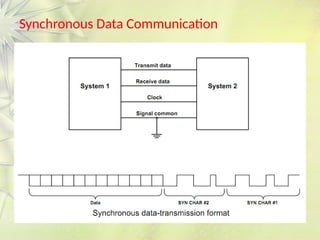
  • 51. Synchronous Vs Asynchronous • Asynchronous transfer does not require clock signal. • However, it transfers extra bits(start bits and stop bits) during data communication. • Synchronous does not transfer extra bits. However, it requires clock signal.
  • 54. 8251 USART • The 8251 USART (Universal Synchronous Asynchronous Receiver Transmitter) is capable of implementing either an asynchronous or synchronous serial data communication. • As a peripheral device of a microcomputer system, the 8251 receives parallel data from the CPU and transmits serial data after conversion. • This device also receives serial data from the outside and transmits parallel data to the CPU after conversion.
  • 57. Pin Description • D0 - D7 - This is bidirectional data bus which receive control words and transmits data from the CPU and sends status words and received data to CPU. • RESET - A "High" on this input forces the 8251 into "reset status”. The min. reset width is six clock inputs during the operating status of CLK. • CLK - CLK signal is used to generate internal device timing. CLK signal is independent of RXC or TXC. • WR - This is the "active low" input terminal which receives a signal for writing transmit data and control words from the CPU into the 8251.
  • 58. Pin Description • RD - This is the "active low" input terminal which receives a signal for reading receive data and status words from the 8251. • C/D - This is an input terminal which receives a signal for selecting data or command words and status words when the 8251 is accessed by the CPU. • CS - This is the "active low" input terminal which selects the 8251 at low level when the CPU accesses.
  • 59. Pin Description • TXD - This is an output terminal for transmitting data from which serial-converted data is sent out. • TXRDY - This is an output terminal which indicates that the 8251 is ready to accept a transmitted data character. • TXEMPTY - This is an output terminal which indicates that the 8251 has transmitted all the characters and had no data character. • TXC - This is a clock input signal (Active Low) which determines the transfer speed of transmitted data. – In "synchronous mode," the baud rate will be the same as the frequency of TXC. In "asynchronous mode", it is possible to select the baud rate factor by mode instruction. It can be 1, 1/16 or 1/64 the TXC.
  • 60. Pin Description • RXD - This is a terminal which receives serial data. • RXRDY - This is a terminal which indicates that the 8251 contains a character that is ready to READ. – If the CPU reads a data character, RXRDY will be reset by the leading edge of RD signal. Unless the CPU reads a data character before the next one is received completely, the preceding data will be lost. In such a case, an overrun error flag status word will be set. • RXC - This is a clock input signal which determines the transfer speed of received data. – In "synchronous mode," the baud rate is the same as the frequency of RXC. In "asynchronous mode," it is possible to select the baud rate factor by mode instruction. It can be 1, 1/16, 1/64 the RXC.
  • 61. Pin Description • SYNDET/BD - This is a terminal whose function changes according to mode. – In “internal synchronous mode“, this terminal is at high level, if sync characters are received and synchronized. – If a status word is read, the terminal will be reset. – In “external synchronous mode”, this is an input terminal. A "High" on this input forces the 8251 to start receiving data characters. – In “asynchronous mode”, this is an output terminal which generates "high level“ output upon the detection of a "break" character if receiver data contains a "low-level" space between the stop bits of two continuous characters. – The terminal will be reset, if RXD is at high level. After Reset is active, the terminal will be output at low level.
  • 62. Pin Description • DSR - This is an input port for MODEM interface. The input status of the terminal can be recognized by the CPU reading status words. • DTR - This is an output port for MODEM interface. It is possible to set the status of DTR by a command. • CTS - This is an input terminal for MODEM interface which is used for controlling a transmit circuit. – The terminal controls data transmission if the device is set in "TX Enable" status by a command. Data is transmittable if the terminal is at low level. • RTS - This is an output port for MODEM interface. It is possible to set the status RTS by a command.
  • 63. 8251 functional configuration • The 8251 functional configuration is programmed by software. • Operation between the 8251 and a CPU is executed by program control. • Table 1 shows the operation between a CPU and the device.
  • 64. Simple Serial I/O Procedures
  • 65. 8251 Control Words • There are two types of control word. 1. Mode instruction (setting of function) 2. Command (setting of operation) • Apart from the control words, a Status Word is present in 8251 to see the internal status.
  • 66. 1. Mode instruction word • Mode instruction is used for setting the function of the 8251. • Mode instruction will be in "wait for write" at either internal reset or external reset. • That is, the writing of a control word after resetting will be recognized as a "mode instruction.“ • Items set by mode instruction are as follows: – Synchronous/asynchronous mode – Stop bit length (asynchronous mode) – Character length – Parity bit – Baud rate factor (asynchronous mode) – Internal/external synchronization (synchronous mode) – Number of synchronous characters (Synchronous mode)
  • 67. Mode Instruction - Asynchronous
  • 68. Mode Instruction - Synchronous
  • 69. 2. Command Word • Command is used for setting the operation of the 8251. • It is possible to write a command whenever necessary after writing a mode instruction and sync characters. • Items to be set by command are as follows: – Transmit Enable/Disable – Receive Enable/Disable – DTR, RTS Output of data. – Resetting of error flag. – Sending to break characters – Internal resetting – Hunt mode (synchronous mode)
  • 72. RS232 • RS-232 (Recommended standard-232) is a standard interface approved by the Electronic Industries Association (EIA) for connecting serial devices. • In other words, RS-232 is a long established standard that describes the physical interface and protocol for relatively low-speed serial data communication between computers and related devices.
  • 73. Limitations of RS-232  Firstly, the interface presupposes a common ground between the DTE and DCE.  Secondly, a signal on a single line is impossible to screen effectively for noise  Low capacitance cable can reduce crosstalk.  Higher frequency that are the problem, control of slew rate in the signal (i.e., making the signal more rounded, rather than square) also decreases the crosstalk.  Voltage levels with respect to ground represent the RS 232 signals.  Interface is useful for point-to-point communication at slow speeds.  Port COM1 in a PC can be used for a mouse, port COM2 for a modem, etc.  Implies limited cable length - about 30 to 60 meters maximum. (Main problems are interference and resistance of the cable.)  Shortly, RS 232 was designed for communication of local devices, and supports one transmitter and one receiver.
  • 75. Direct memory access • Direct memory access (DMA) is a process in which an external device takes over the control of system bus from the CPU. • DMA is for high-speed data transfer from/to mass storage peripherals, e.g. hard disk drive, magnetic tape, CD-ROM, and sometimes video controllers. • The basic idea of DMA is to transfer blocks of data directly between memory and peripherals. • The data don’t go through the microprocessor but the data bus is occupied.
  • 76. Basic process of DMA – Minimum Mode • The HOLD and HLDA pins are used to receive and acknowledge the hold request respectively. • Normally the CPU has full control of the system bus. • In a DMA operation, the peripheral takes over bus control temporarily.
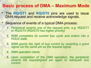
  • 77. Basic process of DMA – Maximum Mode • The RQ/GT1 and RQ/GT0 pins are used to issue DMA request and receive acknowledge signals. • Sequence of events of a typical DMA process: 1. Peripheral asserts one of the request pins, e.g. RQ/GT1 or RQ/GT0 (RQ/GT0 has higher priority) 2. 8086 completes its current bus cycle and enters into a HOLD state. 3. 8086 grants the right of bus control by asserting a grant signal via the same pin as the request signal. 4. DMA operation starts. 5. Upon completion of the DMA operation, the peripheral asserts the request/grant pin again to relinquish bus control.
  • 78. DMA controller • A DMA controller interfaces with several peripherals that may request DMA. • The controller decides the priority of simultaneous DMA requests communicates with the peripheral and the CPU, and provides memory addresses for data transfer. • DMA controller commonly used with 8086 is the 8257/8237 programmable device. • The 8257/8237 is a 4-channel device. • Each channel is dedicated to a specific peripheral device and capable of addressing 64 K bytes section of memory.
  • 79. 8237 - DMA Controller
  • 81. 8237 Registers 1. Current address register 2. Current word register 3. Command register 4. Mode register 5. Request register 6. Mask register 7. Status register 8. Temporary register
  • 82. 8237 Registers 1.Current address register • One 16-bit register for each channel • Holds address for the current DMA transfer 2.Current word register • Keeps the byte count • Generates terminal count (TC) signal when the count goes from zero to FFFFH 3.Command register • Used to program 8257
  • 83. 8237 Registers 4.Mode register • Each channel can be programmed to – Read or write – Autoincrement or autodecrement the address – Autoinitialize the channel 5.Request register • For software-initiated DMA 6.Mask register • Used to disable a specific channel 7.Status register 8.Temporary register • Used for memory-to-memory transfers
  • 84. Keyboard Interface • In most keyboards, the key switches are connected in a matrix of Rows and Columns. • Getting meaningful data from a keyboard requires three major tasks: 1. Detect a key press 2. Debounce the key press. 3. Encode the key press (produce a standard code for the pressed key). • Logic ‘0’ is read by the microprocessor when the key is pressed.
  • 85. Keyboard Interface(Contd…) Key Debounce: Whenever a mechanical push-bottom is pressed or released once, the mechanical components of the key do not change the position smoothly; rather it generates a transient response. These may be interpreted as the multiple pressures and responded accordingly.
  • 88. Keyboard Interface(Contd…) – the 82C55 is decoded at I/O ports 50H–53H for an 8086 – port A is programmed as an input port to read the rows – port B is programmed as an output port to select a column – a flowchart of the software required to read a key from the keyboard matrix and debounce the key is illustrated in Fig.
  • 90. Keyboard Interface(Contd…) – keys must be debounced, normally with a time delay of 10–20 ms – the software uses a procedure called SCAN to scan the keys and another called DELAY10 to waste 10 ms of time for debouncing – the main keyboard procedure is called KEY and appears in Example. – the KEY procedure is generic, and can handle any configuration from a 1  1 matrix to an 8  8 matrix.
  • 91. 8 Digit LED Display
  • 92. 7 segment display a b c g d e f Digit-abcdefg-hex 0-1111110-7E 1-0110000-30 2-1101101-6D 3-1111001-79 4-0110011-33 5-1011011-5B 6-1011111-5F 7-1110000-70 8-1111111-7F 9-1111011-7B A-1110111-77 B-0011111-1F C-1001110-4E D-0111101-3D E-1001111-4F F-1000111-47
  • 93. Stepper Motor Interface Fig.1 Internal schematic of a four winding stepper motor Fig.2 Winding arrangement of a stepper motor. Contd…
  • 95. •A simple scheme for rotating the shaft of a stepper motor is called a wave scheme •In this scheme, windings Wa,Wb, Wc and Wd are applied with the required voltage pulses, in a cyclic fashion. •By reversing the sequence of excitation, the direction of rotation of the stepper motor shaft may be reversed. Table below shows the excitation sequences for clockwise and anticlockwise rotations.
  • 96. Example: •Design a stepper motor controller and write an ALP to rotate shaft of a 4-phase stepper motor •(i) in clockwise 5 rotations •(ii) in anticlockwise 5 rotations •The 8255 port A address is 0740h. The stepper has 200 rotor teeth •The port A bit PA0 drives winding Wa, PA1 drives Wb and so on. •The stepper motor has an initial delay of 10 msec. Assume that the routine for this delay is already available
  • 99. Clockwise: MOV DX,0FFE6 MOV AL,80 OUT DX,AL MOV CX,0FFFF MOV DX,OFFE0 MOV AL,11 X:OUT DX,AL CALL DELAY ROR AL,1 LOOP X DELAY:MOV BX,0FFF Y:DEC BX JNZ Y RET ANTICLOCKWISE: MOV DX,0FFE6 MOV AL,80 OUT DX,AL MOV CX,0FFFF MOV DX,OFFE0 MOV AL,11 X:OUT DX,AL CALL DELAY ROL AL,1 LOOP X DELAY:MOV BX,0FFF Y:DEC BX JNZ Y RET
  • 100. Interfacing Analog to Digital Data Converters General algorithm for ADC interfacing contains the following steps: • Ensure the stability of analog input, applied to the ADC. • Issue start of conversion pulse to ADC • Read end of conversion signal to mark the end of conversion processes. • Read digital data output of the ADC as equivalent digital output. • Analog input voltage must be constant at the input of the ADC right from the start of conversion till the end of the conversion to get correct results. This may be ensured by a sample and hold circuit which samples the analog signal and holds it constant for specific time duration. The microprocessor may issue a hold signal to the sample and hold circuit. • If the applied input changes before the complete conversion process is over, the digital equivalent of the analog input calculated by the ADC may not be correct.
  • 101. Interfacing Analog to Digital Data Converters Fig.1 Block Diagram of ADC 0808/0809 Contd…
  • 102. Interfacing Analog to Digital Data Converters Fig.2 Pin Diagram of ADC 0808/0809 Fig.3 Timing Diagram Of ADC 0808. Contd…
  • 103. Interfacing Analog to Digital Data Converters Fig: Interfacing ADC0808 with 8086 Contd…
  • 104. Interfacing Digital To Analog Converters Pin Diagram of DAC 0800 Contd…
  • 105. Interfacing Digital To Analog Converters Fig:Interfacing DAC0800 with 8086
  • 106. Square Wave A 3000 // (starting address) MOV AL,80 MOV DX,0FFE6 OUT DX,AL MOV DX,0FFE0 XX: MOV AL,00 OUT DX,AL CALL 5000 //(delay address) MOV DX,0FFE0 MOV AL,0FF OUT DX,AL CALL 5000 // (delay address) JMP XX INT 03 DELAY PROGRAM A 5000 //( delay address) MOV CX,00FF YY: LOOP YY RET Triangle Wave A 3000 //(starting address) MOV AL,80 MOV DX,0FFE6 OUT DX,AL XX:MOV AL,0FF YY:MOV DX,0FFE0 OUT DX,AL MOV DX,0FFE2 OUT DX,AL DEC AL JNZ YY ZZ:MOV DX,0FFE2 OUT DX,AL MOV DX,0FFE0 OUT DX,AL INC AL CMP AL,0FF JNZ ZZ JMP XX INT 03
  • 107. Memory Interfacing Design an 8086 based system with the following specifications with each chip of 32kb i) 64kb EPROM II) 64kb Ram. Draw the complete schematic of the design indicating address map. A) 32Kb requires-16 address lines
  • 109. 2) Design an 8086 based system with the following specifications i) 8 Kb EPROM ii) 8KB Ram Draw the complete schematic of the design indicating address map. A) 8Kb requires 13 address lines