1. CS8351 DIGITAL PRINCIPLES AND
SYSTEM DESIGN
UNIT V
MEMORY AND PROGRAMMABLE LOGIC
Prof G ELANGOVAN
Professor and Head
Department of Electrical and Electronics Engineering
NPR College of Engineering and Technology
Natham, Dindigul Dist. 624 401
[email protected]
2. 2
UNIT V
MEMORY AND PROGRAMMABLE
LOGIC
• RAM
• Memory Decoding
• Error Detection and Correction
• ROM
• Programmable Logic Array
• Programmable Array Logic
• Sequential Programmable Devices
3. 3
Introduction
• A memory unit is a collection of storage
cells with associated circuits needed to
transfer information in and out of the device.
• The binary information is transferred for storage
and from which information is available when
needed for processing.
• When data processing takes place, information
from the memory is transferred to selected
registers in the processing unit.
• Intermediate and final results obtained in the
processing unit are transferred back to be stored
in memory.
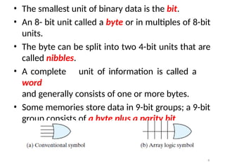
4. • The smallest unit of binary data is the bit.
• An 8- bit unit called a byte or in multiples of 8-bit
units.
• The byte can be split into two 4-bit units that are
called nibbles.
• A complete unit of information is called a
word
and generally consists of one or more bytes.
• Some memories store data in 9-bit groups; a 9-bit
group consists of a byte plus a parity bit.
4
5. Basic Semiconductor Memory Array
• Each storage element in a memory can retain either a 1
or a 0 and is called a cell.
• Memories are made up of arrays of cells,
• Each block in the memory array represents one storage cell,
and its location can be identified by specifying a row and a
column.
5
6. Memory Address and Capacity
• The location of a unit of data in a memory array is called its
address.
• The capacity of a memory is the total number of data units
that can be stored.
6
7. 7
Basic Memory Operations
• Since a memory stores binary data, data must be put
into the memory and data must be copied from the
memory when needed.
• The write operation puts data into a specified address
in the memory, and the read operation copies data out
of a specified address in the memory.
• The addressing operation, which is part of both the
write and the read operations, selects the specified
memory address.
• Data units go into the memory during a write operation
and come out of the memory during a read operation
on a set of lines called the data bus.
• For a write or a read operation, an address is selected
by placing a binary code representing the desired
address on a set of lines called the address bus.
8. • A 15- bit address code can select 32,768 locations (215)
in the memory; a 16-bit address code can select 65,536
locations (216) in the memory and so on.
• In personal computers a 32-bit address bus can select
4,294,967,296 locations (232), expressed as 4GB
Block diagram of memory operation
8
11. 11
Classification of Memories
• Random-Access Memory (RAM)
• RAM (random-access memory) is a type of memory in
which all addresses are accessible in an equal amount
of time and can be selected in any order for a read or
write operation. All RAMs have both read and write
capability. Because RAMs lose stored data when the
power is turned off, they are volatile memories.
• Read-Only Memory (ROM)
• ROM (read-only memory) is a type of memory in which
data are stored permanently or semi permanently.
Data can be read from a ROM, but there is no write
operation as in the RAM. The ROM, like the RAM, is a
random-access memory but the term RAM traditionally
means a random-access read/write memory. Because
ROMs retain stored data even if power is turned off,
they are nonvolatile memories.
13. 13
RAM
• RAMs are read/write memories
• When a data unit is written into a given address,
previously stored data is replaced by the new data unit.
• When a data unit is read from a given address in the
RAM, the data unit remains stored and is not erased by
the read operation.
• This nondestructive read operation can be viewed as
copying the content of an address while leaving the
content intact.
• A RAM is typically used for short-term data storage
because it cannot retain stored data when power is
turned off.
14. 14
• Static RAM (SRAM)
Flip-flops as storage elements and can therefore store
data indefinitely as long as dc power is applied.
• Dynamic RAM (DRAM).
Capacitors as storage elements and cannot retain data
very long without the capacitors being recharged by a
process called refreshing.
• Both SRAMs and DRAMs will lose stored data when dc
power is removed and, therefore, are classified as
volatile memories.
• Data can be read much faster from SRAMs than from
DRAMs.
• However, DRAMs can store much more data than
SRAMs for a given physical size and cost because the
DRAM cell is much simpler, and more cells can be
crammed into a given chip area than in the SRAM.
15. 15
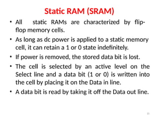
Static RAM (SRAM)
• All static RAMs are characterized by flip-
flop memory cells.
• As long as dc power is applied to a static memory
cell, it can retain a 1 or 0 state indefinitely.
• If power is removed, the stored data bit is lost.
• The cell is selected by an active level on the
Select line and a data bit (1 or 0) is written into
the cell by placing it on the Data in line.
• A data bit is read by taking it off the Data out line.
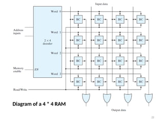
16. Basic Static Memory Cell Array
• The memory cells in a SRAM are organized in rows and
columns.
• All the cells in a row share the same Row Select line.
• Each set of Data in and Data out lines go to each cell in a
given column and are connected to a single data line that
serves as both an input and output (Data I/O) through the
data input and data output buffers.
• SRAM chips can be organized in single bits, nibbles (4 bits),
bytes (8 bits), or multiple bytes (16, 24, 32 bits, etc.).
• 256 rows and 128 columns, each with
8 bits.
16
• There are
actually
215 = 32,768
addresses and each address contains
8 bits.
• The capacity is 32,768 bytes (typically
expressed as 32 Kbytes).
18. 18
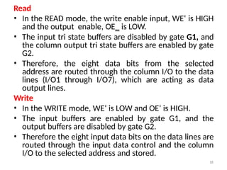
Read
• In the READ mode, the write enable input, WE‘ is HIGH
and the output enable, OE‗ is LOW.
• The input tri state buffers are disabled by gate G1, and
the column output tri state buffers are enabled by gate
G2.
• Therefore, the eight data bits from the selected
address are routed through the column I/O to the data
lines (I/O1 through I/O7), which are acting as data
output lines.
Write
• In the WRITE mode, WE‘ is LOW and OE‘ is HIGH.
• The input buffers are enabled by gate G1, and the
output buffers are disabled by gate G2.
• Therefore the eight input data bits on the data lines are
routed through the input data control and the column
I/O to the selected address and stored.
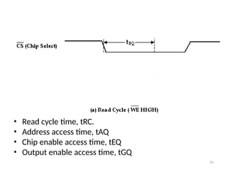
19. • Read cycle time, tRC.
• Address access time, tAQ
• Chip enable access time, tEQ
• Output enable access time, tGQ
19
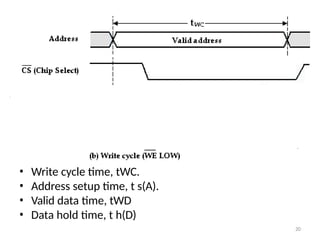
20. • Write cycle time, tWC.
• Address setup time, t s(A).
• Valid data time, tWD
• Data hold time, t h(D)
20
21. Memory Decoding
• Decoding circuits are needed to select the
memory word specified by the input address.
Internal Construction
• A RAM of m words and n bits per word consists of
m * n binary storage cells and associated
decoding circuits for selecting individual words
21
23. 23
• A memory with 2k words of n bits per word requires k
address lines that go into a k * 2k decoder.
• Each one of the decoder outputs selects one word of n bits
for reading or writing.
Coincident Decoding
• A decoder with k inputs and 2k outputs requires 2k AND
gates with k inputs per gate.
• The total number of gates and the number of inputs per
gate can be reduced by employing two decoders in a
two dimensional
‐ selection scheme.
• The basic idea in two dimensional
‐ decoding is to arrange
the memory cells in an array that is close as possible to
square.
• In this configuration, two k /2 input
‐ decoders are used
instead of one k input
‐ decoder.
• One decoder performs the row selection and the other the
column selection in a two dimensional
‐ matrix
configuration.
25. 25
Address Multiplexing
• DRAMs typically have four times the density of SRAMs.
• This allows four times as much memory capacity to be
placed on a given size of chip.
• Because of their large capacity, the address decoding of
DRAMs is arranged in a two dimensional
‐ array, and
larger memories often have multiple arrays.
• To reduce the number of pins in the IC package,
designers utilize address multiplexing whereby one set
of address input pins accommodates the address
components.
• In a two dimensional
‐ array, the address is applied in
two parts at different times, with the row address first
and the column address second.
• Since the same set of pins is used for both parts of the
address, the size of the package is decreased
significantly.
27. Error Detection and Correction
• The most common error detection scheme is the parity bit.
• A parity bit is generated and stored along with the data word
in memory.
• The parity of the word is checked after reading it
from memory.
• The data word is accepted if the parity of the bits read out is
correct.
• If not, an error is detected, but it cannot be corrected.
• An error correcting
‐ code generates multiple parity check
bits that are stored with the data word in memory.
• When the word is read back from memory, the
associated parity bits are also read from memory and
compared with a new set of check bits generated from the
data that have been read.
• If the check bits are correct, no error has occurred.
• If the check bits do not match the stored parity, they
generate a unique pattern, called a syndrome, that can be
used to
identify the bit that is in error. 27
28. 28
Hamming Code
• k parity bits are added to an n bit
‐ data word,
forming a new word of n + k bits.
• The bit positions are numbered in
sequence from 1 to n + k.
• Those positions numbered as a power of 2 are
reserved for the parity bits.
• The remaining bits are the data bits.
• The code can be used with words of
any length
29. Consider, for example, the 8 bit
‐ data word
11000100. We include 4 parity bits with the
8 bit
‐ word and arrange the 12 bits as follows
11
Bit position: 1 2 3 4 5 6 7 8 9 10 11
12
P1 P2 1 P4 1 0 0
P8 0 1 0 0
Each parity bit is calculated as follows
241 0101001
010101
29
65
011001
7 0111
1
9
2
1
1
1
0
01
1010
353
8
1000
9 1001
10 1010
11 1011
12 1100
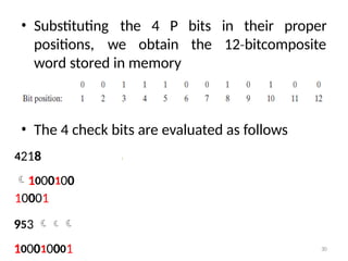
30. • Substituting proper
positions, we obtain
the 4 P bits in their
the 12 bitcomposite
‐
word stored in memory
• The 4 check bits are evaluated as follows
30
4218
1000100
10001
953
100010001
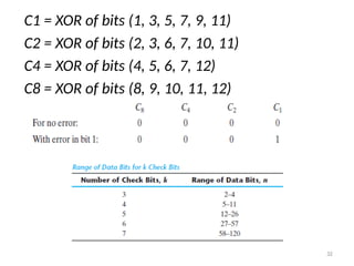
31. • IF result, C = C8C4C2C1 = 0000, indicates that
no error has occurred.
• However, if C ≠ 0, then the 4 bit
‐ binary
number formed by the check bits gives
the position of the erroneous bit.
• For example, consider the following three
cases:
31
33. • The Hamming code is received as 101101101. Correct it if any
errors. There are four parity bits and odd parity is used.
Received data is 101101101
1 2 3 4 5 6 7 8 9
1 0 1 1 0 1 1 0 1
P1 P2 P4 P8
Odd parity is used
C1= XOR of bits (1, 3, 5, 7, 9) = 1, 1, 0, 1, 1 error since even 1s
1
C2= XOR of bits (2, 3, 6, 7) = 0, 1, 1, 1 odd No of 1s 0
C4= XOR of bits (4, 5, 6, 7) = 1, 0, 1, 1 odd No of 1s 0
C8= XOR of bits (8, 9) = 0, 1 odd No of 1s 0
C= C8 C4 C2 C1 = 0001 Bit no 1 has
error
Correct code is 0 0 11 0 1 101 33
34. 34
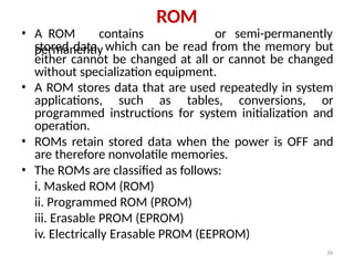
ROM
• A ROM contains
permanently
or semi-permanently
stored data, which can be read from the memory but
either cannot be changed at all or cannot be changed
without specialization equipment.
• A ROM stores data that are used repeatedly in system
applications, such as tables, conversions, or
programmed instructions for system initialization and
operation.
• ROMs retain stored data when the power is OFF and
are therefore nonvolatile memories.
• The ROMs are classified as follows:
i. Masked ROM (ROM)
ii. Programmed ROM (PROM)
iii. Erasable PROM (EPROM)
iv. Electrically Erasable PROM (EEPROM)
35. Masked ROM
• The mask ROM is usually referred to simply as a ROM.
• It is permanently programmed during the manufacturing
process to provide widely used standard functions, such as
popular conversions, or to provide user-specified functions.
• Once the memory is programmed, it cannot be changed.
• Most IC ROMs utilize the presence or absence of a
to
transistor connection at a row/column junction
represent a 1 or a 0.
ROM Cells
35
36. 36
PROM (Programmable Read-Only Memory)
• It comes from the manufacturer unprogrammed and
are custom programmed in the field to meet the user‘s
needs.
• A PROM uses some type of fusing process to store bits,
in which a memory link is burned open or left intact to
represent a 0 or a 1. The fusing process is irreversible;
once a PROM is programmed, it cannot be changed.
• The fusible links are manufactured into the PROM
between the source of each cell's transistor and its
column line. In the programming process, a sufficient
current is injected through the fusible link to bum it
open to create a stored 0. The link is left intact for a
stored 1.
nichrome
polycrystalline silicon
Metal links
Silicon links
Shorted junction
38. 38
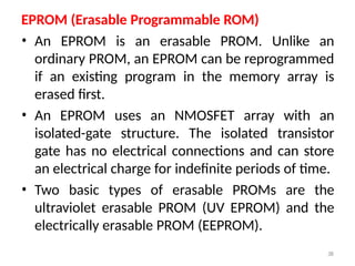
EPROM (Erasable Programmable ROM)
• An EPROM is an erasable PROM. Unlike an
ordinary PROM, an EPROM can be reprogrammed
if an existing program in the memory array is
erased first.
• An EPROM uses an NMOSFET array with an
isolated-gate structure. The isolated transistor
gate has no electrical connections and can store
an electrical charge for indefinite periods of time.
• Two basic types of erasable PROMs are the
ultraviolet erasable PROM (UV EPROM) and the
electrically erasable PROM (EEPROM).
39. 39
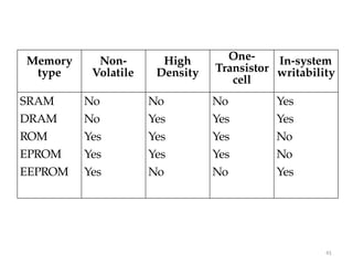
S.No RAM ROM
1
RAMs have both read
and write
capability.
ROMs have only
read operation.
2 RAMs are volatile
memories.
ROMs are non-volatile
memories.
3
They lose stored data
when the
power is turned OFF.
They retain stored data
even if power is
turned off.
4
RAMs are available in
both
bipolar and
MOS technologies.
RAMs are available in both
bipolar and
MOS technologies.
5 Types: SRAM, DRAM,
EEPROM
Types: PROM, EPROM.
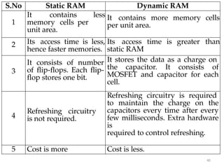
40. 40
S.No Static RAM Dynamic RAM
1
It contains less
memory cells per
unit area.
It contains more memory cells
per unit area.
2 Its access time is less,
hence faster memories.
Its access time is greater than
static RAM
3
It consists of number
of flip-flops. Each flip-
flop stores one bit.
It stores the data as a charge on
the capacitor. It consists of
MOSFET and capacitor for each
cell.
4
Refreshing circuitry
is not required.
Refreshing circuitry is required
to maintain the charge on the
capacitors every time after every
few milliseconds. Extra hardware
is
required to control refreshing.
5 Cost is more Cost is less.
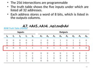
42. ROM block diagram
Internal logic of a 32 : 8 ROM
32 words
of 8 bits each
32 * 8 = 256
internal
connections
42
43. • The 256 intersections are programmable
• The truth table shows the five inputs under which are
listed all 32 addresses.
• Each address stores a word of 8 bits, which is listed in
the outputs columns.
A7, AA65,,AA34, ,Aa2,nadnAd
1A0arFeusmesatrokbeedBwLOitWh Na X
43
45. 45
Combinational Circuit Implementation
2k
• A decoder generates the minterms of the k
input
variables.
• By inserting OR gates to sum the minterms of Boolean
functions, we were able to generate any desired
combinational circuit.
• The ROM is essentially a device that includes both the
decoder and the OR gates within a single device to form a
minterm generator.
• By choosing connections for those minterms which are
included in the function, the ROM outputs can be
programmed to represent the Boolean functions of the
output variables in a combinational circuit.
• The internal operation of a ROM can be interpreted in two
ways.
• The first interpretation is that of a memory unit that
contains a fixed pattern of stored words.
• The second interpretation is that of a unit which
implements a combinational circuit.
46. • Design a combinational circuit using a ROM,
that accepts a 3-bit number and generates
an output binary number equal to the
square of
the given input number
Truth Table for square of the given input number
46
B0 is always equal to input A0
B1 is always 0
47. The minimum size of ROM needed must have
three inputs and four outputs.
Three inputs specify eight words, so the ROM
must be of size 8 * 4.
47
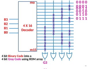
49. 4 bit Binary Code into a
4 bit Gray Code using ROM array
G3
49
B3
B2
B1
B0
mo
m15
4 X 16
Decoder
X
X
X
X
X
X
X
X
X
X
X
X
X
X
X
X
X
X
X
X
X
X
X X
X
X
X
X
X
X
X
0 0 0 0
0 0 0 1
0 0 1 1
0 0 1 0
0 1 1 0
0 1 1 1
50. Implement the following function with ROM.
F1 (A,B,C)=∑m(0,3,7) and f2 (A,B,C)=∑m(1,5,7)
A2 A1 A0 f1
f2
0 0 0 1 0
0 0 1 0 1
0 1 0 0 0
0 1 1 1 0
1 0 0 0 0
1 0 1 0 1
1 1 0 0 0
1 1 1 1 1
ROM truth table and Block
diagram 50
52. 52
Programmable Logic Devices - PLDs
• PLD is an integrated circuit with programmable gates divided into
an AND array and an OR array to provide an AND-OR sum of
product implementation.
• The PLD‘s can be reprogrammed in few seconds and hence gives
more flexibility to experiment with designs.
• Reprogramming feature of PLDs also makes it possible to accept
changes/modifications in the previously design circuits.
• The advantages of using programmable logic devices are:
1. Reduced space requirements.
2. Reduced power requirements.
3. Design security.
4. Compact circuitry.
5. Short design cycle.
6. Low development cost.
7. Higher switching speed.
8. Low production cost for large-quantity production.
53. 53
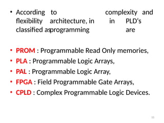
• According
flexibility
to
architecture, in
programming
complexity and
in PLD‘s
are
classified as
• PROM : Programmable Read Only memories,
• PLA : Programmable Logic Arrays,
• PAL : Programmable Logic Array,
• FPGA : Field Programmable Gate Arrays,
• CPLD : Complex Programmable Logic Devices.
55. 55
Programmable Arrays
• All PLDs consists of programmable arrays.
• A programmable array is essentially a grid of
conductors that form rows and columns with a
fusible link at each cross point.
• Arrays can be either fixed or programmable.
The OR Array
It consists of an array of OR gates connected to a
programmable matrix with fusible links at each
cross point of a row and column
The AND Array
This type of array consists of AND gates
connected to a programmable matrix with fusible
links at each cross points
56. An example
of a basic
programmable
OR array
56
An example
of a basic
programmable
AND array
57. 57
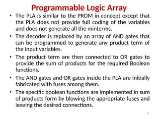
Programmable Logic Array
• The PLA is similar to the PROM in concept except that
the PLA does not provide full coding of the variables
and does not generate all the minterms.
• The decoder is replaced by an array of AND gates that
can be programmed to generate any product term of
the input variables.
• The product term are then connected to OR gates to
provide the sum of products for the required Boolean
functions.
• The AND gates and OR gates inside the PLA are initially
fabricated with fuses among them.
• The specific boolean functions are implemented in sum
of products form by blowing the appropriate fuses and
leaving the desired connections.
59. 59
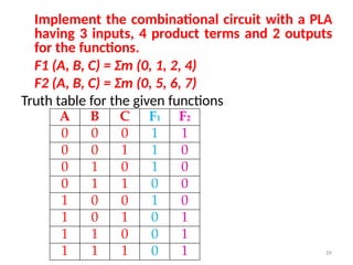
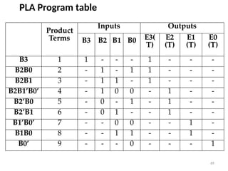
Implement the combinational circuit with a PLA
having 3 inputs, 4 product terms and 2 outputs
for the functions.
F1 (A, B, C) = Σm (0, 1, 2, 4)
F2 (A, B, C) = Σm (0, 5, 6, 7)
Truth table for the given functions
A B C F1 F2
0 0 0 1 1
0 0 1 1 0
0 1 0 1 0
0 1 1 0 0
1 0 0 1 0
1 0 1 0 1
1 1 0 0 1
1 1 1 0 1
60. K-map Simplification
With this simplification, total number of product
term is 6. But we require only 4 product terms.
Therefore find out F1‘ and F2‘.
Now select, F1‘ and F2, the product terms are AC,
AB, BC and A‘B‘C‘ 60
63. 63
Implement the combinational circuit with a PLA
having 3 inputs, 4 product terms and 2 outputs
for the functions.
F1 (A, B, C) = Σm (3, 5, 6, 7)
F2 (A, B, C) = Σm (0, 2, 4, 7)
Truth table for the given functions
A B C F1 F2
0 0 0 0 1
0 0 1 0 0
0 1 0 0 1
0 1 1 1 0
1 0 0 0 1
1 0 1 1 0
1 1 0 1 0
1 1 1 1 1
64. K-map Simplification
With this simplification, total number of product term is
6. But we require only 4 product terms. Therefore find
out F1‘ and F2‘.
Now select, F1‘ and F2, the product terms are B’C’,
A’C’, A’B’ and ABC.
64
71. 71
Programmable Array Logic
• The PAL is a programmable logic device with a
fixed OR array and a programmable AND array.
• Because only the AND gates are programmable,
the PAL is easier to program than, but is not as
flexible as, the PLA.
• A typical PAL with four inputs and four outputs.
• Each input has a buffer–inverter gate, and each
output is generated by a fixed OR gate.
• There are four sections in the unit, each
composed of an AND–OR array that is three
wide, the term used to indicate that there are
three programmable AND gates in each section
and one fixed OR gate.
73. 73
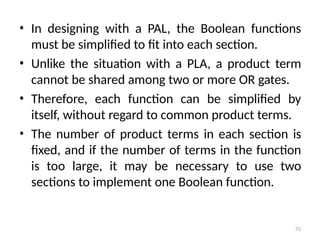
• In designing with a PAL, the Boolean functions
must be simplified to fit into each section.
• Unlike the situation with a PLA, a product term
cannot be shared among two or more OR gates.
• Therefore, each function can be simplified by
itself, without regard to common product terms.
• The number of product terms in each section is
fixed, and if the number of terms in the function
is too large, it may be necessary to use two
sections to implement one Boolean function.
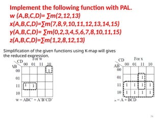
74. Implement the following function with PAL.
w (A,B,C,D)= ∑m(2,12,13)
x(A,B,C,D)=∑m(7,8,9,10,11,12,13,14,15)
y(A,B,C,D)= ∑m(0,2,3,4,5,6,7,8,10,11,15)
z(A,B,C,D)=∑m(1,2,8,12,13)
Simplification of the given functions using K-map will gives
the reduced expression.
74
77. 77
S.No PROM PLA PAL
1
AND array is fixed
and OR array
is programmable
Both AND and
OR n arrays
are programmable
OR array is fixed and
AND array
is programmable
2 Cheaper and simpler
to use
Costliest and
complex
Cheaper and simpler
3
All minterms are
decoded
AND array can be
programmed to
get
desired minterms
AND array can be
programmed to
get desired minterms
4
Only Boolean
functions
in standard SOP
form can be
implemented using
PROM
Any Boolean
functionsinSOP
form can
be implemented
using PLA
Any Boolean
functions in SOP
form can be
implemented using
PLA
Comparison between PROM, PLA, and PAL
78. 78
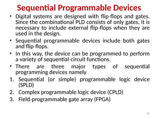
Sequential Programmable Devices
• Digital systems are designed with flip flops
‐ and gates.
Since the combinational PLD consists of only gates, it is
necessary to include external flip flops
‐ when they are
used in the design.
• Sequential programmable devices include both gates
and flip flops.
‐
• In this way, the device can be programmed to perform
a variety of sequential circuit
‐ functions.
• There are three major types of sequential
programming devices namely
1. Sequential (or simple) programmable logic device
(SPLD)
2. Complex programmable logic device (CPLD)
3. Field programmable
‐ gate array (FPGA)
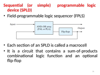
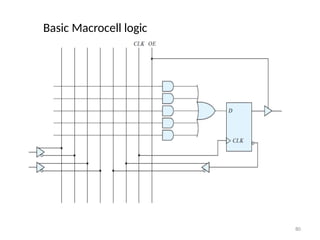
79. Sequential (or simple) programmable logic
device (SPLD)
• Field programmable
‐ logic sequencer (FPLS)
• Each section of an SPLD is called a macrocell
• It is a circuit that contains a sum of products
‐ ‐
combinational logic function and an optional
flip flop
‐
79