SlideShare a Scribd company logo
4
Most read
6
Most read
10
Most read
Unit-6: Introduction to Semiconductor
Manufacturing Process
INTRODUCTION
Objective
The objective of this Unit is:
1.) Introduce the fabrication of integrated circuits
2.) Describe the basic fabrication process steps by which an integrated
circuit is made
Outline
• Integrated circuit fabrication
• Basic processing steps
INTEGRATED CIRCUIT FABRICATION
Classification of Silicon Technology
Silicon IC Technologies
Bipolar Bipolar/MOS MOS
Junction
Isolated
Dielectric
Isolated
Oxide
isolated
CMOS
PMOS
(Aluminum
Gate)
NMOS
Aluminum
gate
Silicon
gate
Aluminum
gate
Silicon
gate
Comparison of Bipolar and CMOS Technologies
Comparison of BJT and MOSFET technology from an analog viewpoint:
Feature BJT MOSFET
Cutoff Frequency(fT) 100 GHz 50 GHz (0.25µm)
Noise (thermal about the same) Less 1/f More 1/f
DC Range of Operation 9 decades of exponential
current versus vBE
2-3 decades of square law
behavior
Small Signal Output Resistance Slightly larger Smaller for short channel
Switch Implementation Poor Good
Capacitor Implementation Voltage dependent Reasonably good
Which is best?
• Almost every comparison favors the BJT, however a similar comparison made from a digital viewpoint
would come up on the side of CMOS.
• Therefore, since large-volume technology will be driven by digital demands, CMOS is an obvious
result as the technology of availability.
Other factors:
• The potential for technology improvement for CMOS is greater than for BJT
• Performance generally increases with decreasing channel length
BiCMOS may be the best compromise for the mixed signal system on a chip.
0.5-0.8mm
n-type: 3-5 -cm
p-type: 14-16 -cm Fig. 2.1-1r
BASIC FABRICATION PROCESSES
Basic steps
• Wafer Cleaning
• Oxide growth
• Thermal diffusion
• Ion implantation
• Deposition
• Etching
• Epitaxy
Photolithography
Photolithography is the means by which the above steps are applied to selected areas
of the silicon wafer.
Silicon wafer
125-200 mm
(5"-8")
For Silicon substrate:-
RCA-1 cleaning has been done to remove the organic contaminants from the wafer. 5 parts
of DI water is mixed with 1 part of ammonia solution and 1 part of hydrogen peroxide [a].
RCA-2 cleaning, in which metal ions or thin oxide layer can be removed from it. 6 parts of
DI water along with 1 part of hydrochloric acid and 1 part of hydro peroxide has been used
for this process [a].
[a] Kern, FW. "Cleaning solutions based on hydrogen peroxide for use in silicon semiconductor technology." RCA
Rev. 31 (1970): 187.
Wafer Cleaning
Oxidation
Description:
Oxidation is the process by which a layer of silicon dioxide is grown on the surface of a
silicon wafer.
Original silicon surface
0.44 tox
tox
Silicon substrate
Silicon dioxide
Fig. 2.1-2
Uses:
• Protect the underlying material from contamination
• Provide isolation between two layers.
Very thin oxides (100Å to 1000Å) are grown using dry oxidation techniques. Thicker oxides (>1000Å)
are grown using wet oxidation techniques.
Diffusion
Diffusion is the movement of impurity atoms at the surface of the silicon into the bulk of the silicon.
Always in the direction from higher concentration to lower concentration.
High
Concentration
Low
Concentration
Fig. 2.1-3
Diffusion is typically done at high temperatures: 800 to 1400°C
ERFC Gaussian
t1 < t2 < t3
t1
t2
t3
Depth (x)
(b) a finite source of impurities at the surface.)
NB
N(x)
t
N(x)
3
NB
t1 < t2 < t3
t1 t2
Depth (x)
(a) Infinite source of impurities at the surface.
N0 N0
Ion Implantation
Ion implantation is the process by which impurity ions are accelerated to a high velocity and
physically lodged into the target material.
Path of
impurity
atom
FixedAtom
FixedAtom
FixedAtom
Impurity Atom
final resting place
Fig. 2.1-5
• Anneal is required to activate the impurity atoms and repair the physical damage to the crystal
lattice. This step is done at 500 to 800°C.
• Ion implantation is a lower temperature process compared to diffusion.
• Can implant through surface layers, thus it is useful for field-
threshold adjustment.
• Can achieve unique doping profile such as buried
concentration peak.
N(
x)
N
B
0 Depth (x)
Concentration peak
Fig. 2.1-
6
Deposition
Deposition is the means by which various materials are deposited on the silicon wafer.
Examples:
• Silicon nitride (Si3N4)
• Silicon dioxide (SiO2)
• Aluminum
• Polysilicon
There are various ways to deposit a material on a substrate:
• Chemical-vapor deposition (CVD)
• Low-pressure chemical-vapor deposition (LPCVD)
• Plasma-assisted chemical-vapor deposition (PECVD)
• Sputter deposition
Material that is being deposited using these techniques cover the entire wafer.
Etching
Etching is the process of selectively removing a layer of material. When etching is
performed, the etchant may remove portions or all of:
• The desired material
• The underlying layer
• The masking layer
Important considerations:
• Anisotropy of the etch is defined as,
A = 1-(lateral etch rate/vertical etch rate)
• Selectivity of the etch (film to mask and film to substrate) is defined as,
Sfilm-mask
=
film etch rate
mask etch rate
Mask
Film
b
a
c
Mask
Film
Underlying layer
(a) Portion of the top layer ready for etching. (b) Horizontal etching and etching of underlying layer.
A = 1 and Sfilm-mask =  are desired.
There are basically two types of etches:
• Wet etch which uses chemicals
• Dry etch which uses chemically active ionized gases.
Fig. 2.1-7 Selectivity
Anisotropy
Underlying layer
Selectivity
Si Si
Si Si Si Si Si Si Si Si Si Si Si Si
Si Si Si Si
Si
+ Si
Si
Si Si Si
Si Si - Si
Si Si Si
Si Si Si
Si Si Si
Si Si
- Si
Si Si Si
Si Si Si
- Si
Si Si Si Si
Si Si Si Si Si Si
- -
-
+
+
Si Si Si Si Si Si
+
Si Si Si Si Si
Si Si
Epitaxy
Epitaxial growth consists of the formation of a layer of single-crystal silicon on the surface of the
silicon material so that the crystal structure of the silicon is continuous across the interfaces.
• It is done externally to the material as opposed to diffusion which is internal
• The epitaxial layer (epi) can be doped differently, even oppositely, of the material on which it
grown
• It accomplished at high temperatures using a chemical reaction at the surface
• The epi layer can be any thickness, typically 1-20 microns
Gaseous cloud containing SiCL4 or SiH4
Si Si Si
Si+
Si Si Si
Fig. 2.1-7.5
Similar results can be obtained through bottom-up and top-down processes
• Top-down approach
• Bottom-up approach
Fabrication Approach
Top Down Process
Clean wafer
Deposit barrier layer
SiO2
Coat with photoresist
Soft bake
Align masks
Expose pattern
Develop photoresist
Hard bake
Etch windows in barrier layer
Remove photoresist
Source: Jaeger, Richard C. (2002). Introduction to Microelectronic
Fabrication (2nd ed.). Prentice Hall. ISBN 0-201-44494-1.
Photolithography
Components
• Photoresist material
• Mask
• Material to be patterned (e.g., oxide)
Positive photoresist
Areas exposed to UV light are soluble in the developer
Negative photoresist
Areas not exposed to UV light are soluble in the developer
Steps
1. Apply photoresist
2. Soft bake (drives off solvents in the photoresist)
3. Expose the photoresist to UV light through a mask
4. Develop (remove unwanted photoresist using solvents)
5. Hard bake (  100°C)
6. Remove photoresist (solvents)
Illustration of Photolithography -
Exposure
The process of exposing selective
areas to light through a photo- mask is
called printing.
Types of printing include:
• Contact printing
• Proximity printing
• Projection printing
Photoresist
Polysilicon
Photomask
UV Light
Photomask
Fig. 2.1-8
Illustration of Photolithography - Positive Photoresist
Photoresist
Photoresist
Polysilicon
Polysilicon
Develop
Polysilicon
Etch
Remove
photoresist
Fig. 2.1-9
Underlying Layer
SiO2
Underlying Layer
Photoresist
Underlying Layer
SiO2
SiO2
Illustration of Photolithography - Negative Photoresist
(Not used much any more)
Photoresist
Fig. 2.1-10
Start with bulk wafer
Alter area of wafer where
structure is to be created
by adding polymer or seed
crystals or other
techniques.
Grow or assemble the
structure on the area
determined by the seed
crystals or polymer.
(self assembly)
Bottom Up Process
 Allows smaller geometries than photolithography.
 Certain structures such as Carbon Nanotubes and Si nanowires are
grown through a bottom-up process.
 New technologies such as organic semiconductors employ bottom-up
processes to pattern them.
 Can make formation of films and structures much easier.
 Is more economical than top-down in that it does not waste material to
etching.
Why is Bottom-Up Processing Needed?
SUMMARY
Fabrication is the means by which the circuit components, both active and
passive, are built as an integrated circuit.
Basic process steps include:
• Oxide growth
• Thermal diffusion
• Ion implantation
• Deposition
• Etching
• Epitaxy
These steps are restricted to a physical area by the use of photolithography.
The use of photolithography to apply a process to a certain area is called a
masking step.
The complexity of a process can be measured in the terms of the number of
masking steps or masks required to implement the process.

More Related Content

PPTX
Wafer processing-1.pptx
PDF
Wafer cleaning
PPT
Wafer manufacturing process
PPTX
Oxidation
PDF
IC Fabrication Process
PPTX
Lecture 8
PPTX
Fabrication process flow
PPTX
Fabrication of Semiconductors
Wafer processing-1.pptx
Wafer cleaning
Wafer manufacturing process
Oxidation
IC Fabrication Process
Lecture 8
Fabrication process flow
Fabrication of Semiconductors

What's hot (20)

PPTX
Oxidation--ABU SYED KUET
PPTX
Dry and wet etching
PPT
Lect5 Diffusion
PPTX
Epitaxy techniques
PPTX
Wafer Fabrication, CZ Method--ABU SYED KUET
PPT
Vlsi design and fabrication ppt
PPTX
Low Pressure Chemical Vapour Deposition
PPTX
VLSI Design(Fabrication)
PDF
Crystal Growth
PPT
Silicon Manufacturing
PPTX
Float Zone, Bridgman Techniques--ABU SYED KUET
PDF
Lecture 2 ic fabrication processing & wafer preparation
PPT
3. crystal growth and wafer fabrication
PPTX
MOSFET fabrication 12
PPTX
New microsoft power point presentation
PPTX
Ion implantation
PPTX
Device isolation Techniques
PDF
Etching
PPTX
Photolithography
Oxidation--ABU SYED KUET
Dry and wet etching
Lect5 Diffusion
Epitaxy techniques
Wafer Fabrication, CZ Method--ABU SYED KUET
Vlsi design and fabrication ppt
Low Pressure Chemical Vapour Deposition
VLSI Design(Fabrication)
Crystal Growth
Silicon Manufacturing
Float Zone, Bridgman Techniques--ABU SYED KUET
Lecture 2 ic fabrication processing & wafer preparation
3. crystal growth and wafer fabrication
MOSFET fabrication 12
New microsoft power point presentation
Ion implantation
Device isolation Techniques
Etching
Photolithography
Ad

Similar to Unit-6 Semiconductor Manufacturing Process.pptx (20)

PPTX
MONOLITHIC IC PROCESSES ppt.pptx
PPTX
Mems unit 1-lec_2
PPT
CMOS Topic 2 -manufacturing_process
PPT
Epitaxial growth
PPTX
Micro Electromechanical system introduction .pptx
PPTX
Planar fabrication technology
PPTX
IC design: Microelectronic Technology.pptx
PPTX
integrated circuit febrication
PPTX
Microsystems Technologies: Basic concepts and terminology
PDF
Electronic Devices - Integrated Circuit.pdf
PPTX
Module-1.pptx
DOCX
Vlsi assembly technology
PPTX
vlsi fabrication
PDF
2.ic fabrication
PDF
Fabrication
PPTX
Chapter 1-IC Fabrication.pptx
PPTX
Lithography, Photolithography--ABU SYED KUET
PPT
Enmater Final Ppt
PPTX
processes involved in the preparation of semiconductor wafers
MONOLITHIC IC PROCESSES ppt.pptx
Mems unit 1-lec_2
CMOS Topic 2 -manufacturing_process
Epitaxial growth
Micro Electromechanical system introduction .pptx
Planar fabrication technology
IC design: Microelectronic Technology.pptx
integrated circuit febrication
Microsystems Technologies: Basic concepts and terminology
Electronic Devices - Integrated Circuit.pdf
Module-1.pptx
Vlsi assembly technology
vlsi fabrication
2.ic fabrication
Fabrication
Chapter 1-IC Fabrication.pptx
Lithography, Photolithography--ABU SYED KUET
Enmater Final Ppt
processes involved in the preparation of semiconductor wafers
Ad

Recently uploaded (20)

PPTX
Infosys Presentation by1.Riyan Bagwan 2.Samadhan Naiknavare 3.Gaurav Shinde 4...
PPT
Mechanical Engineering MATERIALS Selection
PPTX
Sustainable Sites - Green Building Construction
PPTX
Safety Seminar civil to be ensured for safe working.
PDF
Mohammad Mahdi Farshadian CV - Prospective PhD Student 2026
PDF
Unit I ESSENTIAL OF DIGITAL MARKETING.pdf
PPT
introduction to datamining and warehousing
PDF
Embodied AI: Ushering in the Next Era of Intelligent Systems
PPT
Total quality management ppt for engineering students
PPT
Introduction, IoT Design Methodology, Case Study on IoT System for Weather Mo...
PPTX
Engineering Ethics, Safety and Environment [Autosaved] (1).pptx
PDF
Level 2 – IBM Data and AI Fundamentals (1)_v1.1.PDF
DOCX
ASol_English-Language-Literature-Set-1-27-02-2023-converted.docx
PPTX
CYBER-CRIMES AND SECURITY A guide to understanding
PPTX
Fundamentals of safety and accident prevention -final (1).pptx
PDF
BMEC211 - INTRODUCTION TO MECHATRONICS-1.pdf
PPTX
UNIT 4 Total Quality Management .pptx
PDF
III.4.1.2_The_Space_Environment.p pdffdf
PDF
A SYSTEMATIC REVIEW OF APPLICATIONS IN FRAUD DETECTION
PPTX
Foundation to blockchain - A guide to Blockchain Tech
Infosys Presentation by1.Riyan Bagwan 2.Samadhan Naiknavare 3.Gaurav Shinde 4...
Mechanical Engineering MATERIALS Selection
Sustainable Sites - Green Building Construction
Safety Seminar civil to be ensured for safe working.
Mohammad Mahdi Farshadian CV - Prospective PhD Student 2026
Unit I ESSENTIAL OF DIGITAL MARKETING.pdf
introduction to datamining and warehousing
Embodied AI: Ushering in the Next Era of Intelligent Systems
Total quality management ppt for engineering students
Introduction, IoT Design Methodology, Case Study on IoT System for Weather Mo...
Engineering Ethics, Safety and Environment [Autosaved] (1).pptx
Level 2 – IBM Data and AI Fundamentals (1)_v1.1.PDF
ASol_English-Language-Literature-Set-1-27-02-2023-converted.docx
CYBER-CRIMES AND SECURITY A guide to understanding
Fundamentals of safety and accident prevention -final (1).pptx
BMEC211 - INTRODUCTION TO MECHATRONICS-1.pdf
UNIT 4 Total Quality Management .pptx
III.4.1.2_The_Space_Environment.p pdffdf
A SYSTEMATIC REVIEW OF APPLICATIONS IN FRAUD DETECTION
Foundation to blockchain - A guide to Blockchain Tech

Unit-6 Semiconductor Manufacturing Process.pptx

  • 1. Unit-6: Introduction to Semiconductor Manufacturing Process INTRODUCTION Objective The objective of this Unit is: 1.) Introduce the fabrication of integrated circuits 2.) Describe the basic fabrication process steps by which an integrated circuit is made Outline • Integrated circuit fabrication • Basic processing steps
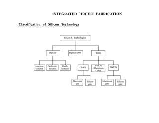
  • 2. INTEGRATED CIRCUIT FABRICATION Classification of Silicon Technology Silicon IC Technologies Bipolar Bipolar/MOS MOS Junction Isolated Dielectric Isolated Oxide isolated CMOS PMOS (Aluminum Gate) NMOS Aluminum gate Silicon gate Aluminum gate Silicon gate
  • 3. Comparison of Bipolar and CMOS Technologies Comparison of BJT and MOSFET technology from an analog viewpoint: Feature BJT MOSFET Cutoff Frequency(fT) 100 GHz 50 GHz (0.25µm) Noise (thermal about the same) Less 1/f More 1/f DC Range of Operation 9 decades of exponential current versus vBE 2-3 decades of square law behavior Small Signal Output Resistance Slightly larger Smaller for short channel Switch Implementation Poor Good Capacitor Implementation Voltage dependent Reasonably good Which is best? • Almost every comparison favors the BJT, however a similar comparison made from a digital viewpoint would come up on the side of CMOS. • Therefore, since large-volume technology will be driven by digital demands, CMOS is an obvious result as the technology of availability. Other factors: • The potential for technology improvement for CMOS is greater than for BJT • Performance generally increases with decreasing channel length BiCMOS may be the best compromise for the mixed signal system on a chip.
  • 4. 0.5-0.8mm n-type: 3-5 -cm p-type: 14-16 -cm Fig. 2.1-1r BASIC FABRICATION PROCESSES Basic steps • Wafer Cleaning • Oxide growth • Thermal diffusion • Ion implantation • Deposition • Etching • Epitaxy Photolithography Photolithography is the means by which the above steps are applied to selected areas of the silicon wafer. Silicon wafer 125-200 mm (5"-8")
  • 5. For Silicon substrate:- RCA-1 cleaning has been done to remove the organic contaminants from the wafer. 5 parts of DI water is mixed with 1 part of ammonia solution and 1 part of hydrogen peroxide [a]. RCA-2 cleaning, in which metal ions or thin oxide layer can be removed from it. 6 parts of DI water along with 1 part of hydrochloric acid and 1 part of hydro peroxide has been used for this process [a]. [a] Kern, FW. "Cleaning solutions based on hydrogen peroxide for use in silicon semiconductor technology." RCA Rev. 31 (1970): 187. Wafer Cleaning
  • 6. Oxidation Description: Oxidation is the process by which a layer of silicon dioxide is grown on the surface of a silicon wafer. Original silicon surface 0.44 tox tox Silicon substrate Silicon dioxide Fig. 2.1-2 Uses: • Protect the underlying material from contamination • Provide isolation between two layers. Very thin oxides (100Å to 1000Å) are grown using dry oxidation techniques. Thicker oxides (>1000Å) are grown using wet oxidation techniques.
  • 7. Diffusion Diffusion is the movement of impurity atoms at the surface of the silicon into the bulk of the silicon. Always in the direction from higher concentration to lower concentration. High Concentration Low Concentration Fig. 2.1-3 Diffusion is typically done at high temperatures: 800 to 1400°C ERFC Gaussian t1 < t2 < t3 t1 t2 t3 Depth (x) (b) a finite source of impurities at the surface.) NB N(x) t N(x) 3 NB t1 < t2 < t3 t1 t2 Depth (x) (a) Infinite source of impurities at the surface. N0 N0
  • 8. Ion Implantation Ion implantation is the process by which impurity ions are accelerated to a high velocity and physically lodged into the target material. Path of impurity atom FixedAtom FixedAtom FixedAtom Impurity Atom final resting place Fig. 2.1-5 • Anneal is required to activate the impurity atoms and repair the physical damage to the crystal lattice. This step is done at 500 to 800°C. • Ion implantation is a lower temperature process compared to diffusion. • Can implant through surface layers, thus it is useful for field- threshold adjustment. • Can achieve unique doping profile such as buried concentration peak. N( x) N B 0 Depth (x) Concentration peak Fig. 2.1- 6
  • 9. Deposition Deposition is the means by which various materials are deposited on the silicon wafer. Examples: • Silicon nitride (Si3N4) • Silicon dioxide (SiO2) • Aluminum • Polysilicon There are various ways to deposit a material on a substrate: • Chemical-vapor deposition (CVD) • Low-pressure chemical-vapor deposition (LPCVD) • Plasma-assisted chemical-vapor deposition (PECVD) • Sputter deposition Material that is being deposited using these techniques cover the entire wafer.
  • 10. Etching Etching is the process of selectively removing a layer of material. When etching is performed, the etchant may remove portions or all of: • The desired material • The underlying layer • The masking layer Important considerations: • Anisotropy of the etch is defined as, A = 1-(lateral etch rate/vertical etch rate) • Selectivity of the etch (film to mask and film to substrate) is defined as, Sfilm-mask = film etch rate mask etch rate Mask Film b a c Mask Film Underlying layer (a) Portion of the top layer ready for etching. (b) Horizontal etching and etching of underlying layer. A = 1 and Sfilm-mask =  are desired. There are basically two types of etches: • Wet etch which uses chemicals • Dry etch which uses chemically active ionized gases. Fig. 2.1-7 Selectivity Anisotropy Underlying layer Selectivity
  • 11. Si Si Si Si Si Si Si Si Si Si Si Si Si Si Si Si Si Si Si + Si Si Si Si Si Si Si - Si Si Si Si Si Si Si Si Si Si Si Si - Si Si Si Si Si Si Si - Si Si Si Si Si Si Si Si Si Si Si - - - + + Si Si Si Si Si Si + Si Si Si Si Si Si Si Epitaxy Epitaxial growth consists of the formation of a layer of single-crystal silicon on the surface of the silicon material so that the crystal structure of the silicon is continuous across the interfaces. • It is done externally to the material as opposed to diffusion which is internal • The epitaxial layer (epi) can be doped differently, even oppositely, of the material on which it grown • It accomplished at high temperatures using a chemical reaction at the surface • The epi layer can be any thickness, typically 1-20 microns Gaseous cloud containing SiCL4 or SiH4 Si Si Si Si+ Si Si Si Fig. 2.1-7.5
  • 12. Similar results can be obtained through bottom-up and top-down processes • Top-down approach • Bottom-up approach Fabrication Approach
  • 14. Clean wafer Deposit barrier layer SiO2 Coat with photoresist Soft bake Align masks Expose pattern Develop photoresist Hard bake Etch windows in barrier layer Remove photoresist Source: Jaeger, Richard C. (2002). Introduction to Microelectronic Fabrication (2nd ed.). Prentice Hall. ISBN 0-201-44494-1.
  • 15. Photolithography Components • Photoresist material • Mask • Material to be patterned (e.g., oxide) Positive photoresist Areas exposed to UV light are soluble in the developer Negative photoresist Areas not exposed to UV light are soluble in the developer Steps 1. Apply photoresist 2. Soft bake (drives off solvents in the photoresist) 3. Expose the photoresist to UV light through a mask 4. Develop (remove unwanted photoresist using solvents) 5. Hard bake (  100°C) 6. Remove photoresist (solvents)
  • 16. Illustration of Photolithography - Exposure The process of exposing selective areas to light through a photo- mask is called printing. Types of printing include: • Contact printing • Proximity printing • Projection printing Photoresist Polysilicon Photomask UV Light Photomask Fig. 2.1-8
  • 17. Illustration of Photolithography - Positive Photoresist Photoresist Photoresist Polysilicon Polysilicon Develop Polysilicon Etch Remove photoresist Fig. 2.1-9
  • 18. Underlying Layer SiO2 Underlying Layer Photoresist Underlying Layer SiO2 SiO2 Illustration of Photolithography - Negative Photoresist (Not used much any more) Photoresist Fig. 2.1-10
  • 19. Start with bulk wafer Alter area of wafer where structure is to be created by adding polymer or seed crystals or other techniques. Grow or assemble the structure on the area determined by the seed crystals or polymer. (self assembly) Bottom Up Process
  • 20.  Allows smaller geometries than photolithography.  Certain structures such as Carbon Nanotubes and Si nanowires are grown through a bottom-up process.  New technologies such as organic semiconductors employ bottom-up processes to pattern them.  Can make formation of films and structures much easier.  Is more economical than top-down in that it does not waste material to etching. Why is Bottom-Up Processing Needed?
  • 21. SUMMARY Fabrication is the means by which the circuit components, both active and passive, are built as an integrated circuit. Basic process steps include: • Oxide growth • Thermal diffusion • Ion implantation • Deposition • Etching • Epitaxy These steps are restricted to a physical area by the use of photolithography. The use of photolithography to apply a process to a certain area is called a masking step. The complexity of a process can be measured in the terms of the number of masking steps or masks required to implement the process.

Editor's Notes

  • #15: Positive Photoresist AZ5214E. Developer:- Alkali solution (whose pH is greater than 7). Resist Removel:- +ve:-Trichloroethylene (TCE), -ve:- Methylethyl Ketone.