


![Four-State VCD fileFour-State VCD file
VCD file format:
20
$date
Fri Sep 05 17:32:13 2014
$end
$version
ModelSim Version 10.1c
$end
$timescale
1ps
$end
$scope module adder_nbit_vcd_tb $end
$scope module UUT $end
$var wire 1 ! sum [3] $end
$var wire 1 " sum [2] $end
$var wire 1 # sum [1] $end
$var wire 1 $ sum [0] $end
$var wire 1 % c_out $end
$var wire 1 & x [3] $end
$var wire 1 ' x [2] $end
$var wire 1 ( x [1] $end
$var wire 1 ) x [0] $end
$var wire 1 * y [3] $end
$var wire 1 + y [2] $end
$var wire 1 , y [1] $end
$var wire 1 - y [0] $end
$var wire 1 . c_in $end
$upscope $end
$upscope $end
$enddefinitions $end
#0
$dumpvars
0$
0#
0"
0!
0%
0.
0)
0(
0'
0&
0-
0,
0+
0*
$end
#5000
1-
1$
#10000
0-
1,
0$
1#
#15000
1-
1$
#20000
$dumpoff
x$
x#
x"
x!
x%
x.
x)
x(
x'
x&
x-
x,
x+
x*
$end](https://image.slidesharecdn.com/verification-141009053122-conversion-gate01/85/Verilog-HDL-Verification-20-320.jpg)


Verilog HDL Verification
- 1. VerificationVerification Gookyi Dennis A. N.Gookyi Dennis A. N. October.07.2014
- 2. ContentsContents Static Timing Analysis 2
- 3. Static Timing AnalysisStatic Timing Analysis Problems with DTA: Poses a bottleneck for large complex designs because simulation requires a lot of time execute Relies on the quality and coverage of testbenches Difficult to figure out critical paths simulations 3
- 4. Fundamentals of STAFundamentals of STA STA determines if a circuit meets timing constraints without having to simulate the design in a cycle to cycle manner It computes the delay for each path of the design and therefore the critical path can easily be found To perform STA, here are some assumptions made: No combinational feedback loops are allowed All register feedback paths must be broken STA is used to verify timing specification but not the functionality of the design 4
- 5. Fundamentals of STAFundamentals of STA In STA, designs are broken into sets of signal paths where each path has a start and an endpoint 4 paths are defined in STA: 5 Path Description Entry Starts at an input port and ends at the data input of a register Stage Starts at the clock input to a register and ends at the data input to another register Exit Starts at the clock input to a register and ends at an output port Pad-to-pad Starts at an input port and ends at an output port D Q D Q Combinational logic Combinational logic Combinational logic Combinational logic Clock Entry path Pad-to-pad path Stage path Exit path
- 6. Timing SpecificationsTiming Specifications The most used timing constraints are divided into: Port related constraints: Input delay (offset-in) Output delay (offset-out) Input-output (pad to pad) Clock related constraints: Clock period Setup time Hold time 6
- 7. Port-Related ConstraintsPort-Related Constraints The various port related constraints include: 7 Delay Description Input Specifies the arrival time of the input signal relative to active edge of the clock Output Specifies the latest time that a signal from the output of a register may reach may reach the output port Input-Output Applies to the path from an input port to an output port without passing through any register D Q D Q Combinational logic Combinational logic Combinational logic Combinational logic Clock Input delay Offset in Offset out Output delay
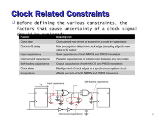
- 8. Clock Related ConstraintsClock Related Constraints Before defining the various constraints, the factors that cause uncertainty of a clock signal should be explored: 8 Factor Description Clock jitter Clock period may shrink or expand on a cycle-by-cycle basis Clock-to-Q delay Max propagation delay from clock edge (sampling edge) to new value of Q output Input capacitance Gate capacitance of both NMOS and PMOS transistors Interconnect capacitance Parasitic capacitances of interconnect between any two nodes Self-loading capacitance Output capacitance of both NMOS and PMOS transistors Clock skew Misalignment of clock edges in a synchronous system circuit temperature Affects currents of both NMOS and PMOS transistors D Q D Q Input capacitance Self-loading capacitance interconnect capacitance Tq
- 9. Clock Related ConstraintsClock Related Constraints The clock related constraints include; Clock period: applies to the path between regs and specifies the max period of the clock of a synchronous circuit Setup time: amount of time that data must be stable before the active clock transition Hold time: amount of time data must remain stable after the active clock transition 9
- 10. Timing AnalysisTiming Analysis After timing specification is given, STA can proceed to measure the critical path Critical path is the path with the longest propagation delay in the design Formally, critical path has a negative or smallest slack time slack time = required time – arrival time Critical path limits system performance 10
- 11. Timing ExceptionsTiming Exceptions Timing analysis tools usually treat all paths in the design as single cycle by default before performing STA In most designs, there are paths that exhibit timing exceptions Two common timing exceptions include False paths Multi-cycle paths 11
- 12. False PathFalse Path A false path is identified as a timing path that does not actually propagate a signal As shown in the diagram below, the path indicated is never activated 12 1 0 1 0 50 ns 100 ns 100 ns 50 ns False path
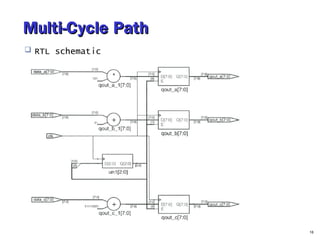
- 13. Multi-Cycle pathMulti-Cycle path In multi-cycle path, data may take more than one clock cycle to reach their destination It is required to indicate which paths are multi- cycle paths in other to avoid false results from the STA 13
- 14. Multi-Cycle pathMulti-Cycle path Example of multi-cycle path (code and testbench) Variable qout_a is updated every clk cycle Variable qout_b is updated every two clk cycles Variable qout_c is updated every three clk cycles 14
- 15. Multi-Cycle PathMulti-Cycle Path Testbench and waveform: 15
- 16. Multi-Cycle PathMulti-Cycle Path RTL schematic 16
- 17. Value Change Dump (VCD) FilesValue Change Dump (VCD) Files A VCD file is a text file that contains information about value changes on selected variables in a design The main purpose is to provide information for debug tools Two types of VCD files include: Four-state VCD file: selected variable changes in {0,1,x,z} without any strength information Extended VCD file: selected variable changes in all states and strength information 17
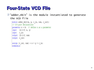
- 18. Four-State VCD FileFour-State VCD File “adder_nbit” is the module instantiated to generate the VCD file 18
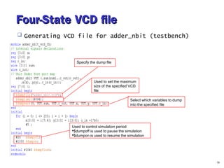
- 19. Four-State VCD fileFour-State VCD file Generating VCD file for adder_nbit (testbench) 19 Specify the dump file Select which variables to dump into the specified file Used to control simulation period $dumpoff is used to pause the simulation $dumpon is used to resume the simulation Used to set the maximum size of the specified VCD file
- 20. Four-State VCD fileFour-State VCD file VCD file format: 20 $date Fri Sep 05 17:32:13 2014 $end $version ModelSim Version 10.1c $end $timescale 1ps $end $scope module adder_nbit_vcd_tb $end $scope module UUT $end $var wire 1 ! sum [3] $end $var wire 1 " sum [2] $end $var wire 1 # sum [1] $end $var wire 1 $ sum [0] $end $var wire 1 % c_out $end $var wire 1 & x [3] $end $var wire 1 ' x [2] $end $var wire 1 ( x [1] $end $var wire 1 ) x [0] $end $var wire 1 * y [3] $end $var wire 1 + y [2] $end $var wire 1 , y [1] $end $var wire 1 - y [0] $end $var wire 1 . c_in $end $upscope $end $upscope $end $enddefinitions $end #0 $dumpvars 0$ 0# 0" 0! 0% 0. 0) 0( 0' 0& 0- 0, 0+ 0* $end #5000 1- 1$ #10000 0- 1, 0$ 1# #15000 1- 1$ #20000 $dumpoff x$ x# x" x! x% x. x) x( x' x& x- x, x+ x* $end
- 21. ISE Design FlowISE Design Flow ISE design flow can be grouped into Design entry Synthesis Implementation Configure FPGA 21
- 22. Design EntryDesign Entry Design entry is based on HDL After a design is entered into the design flow, the functional verification is followed through simulation or formal proof 22
- 23. SynthesisSynthesis Synthesis extract logic from HDL and translates it into an EDIF file (*.edf) The synthesis phase is divided into: 23 Phase Description Parsing Syntax errors are identified Synthesis Extract FSM and identify resources that can be shared Optimization Timing optimization, LUT mapping and register replication
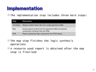
- 24. ImplementationImplementation The implementation step includes three main steps: The map step finishes the logic synthesis operations A resource used report is obtained after the map step is finalized 24 Step Description Translation Merges multiple design files into a single gate-level netlist Map Groups logical symbols from the gate-level netlist into physical components including CLBs and IOBs PAR Places synthesized logic components into FPGA fabrics
- 25. ImplementationImplementation Translation report of “adder_nbit”: 25
- 26. ImplementationImplementation Mapping: The following gives the resource used in module adder_nbit From this report, the feasibility of the design is seen 26
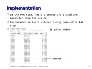
- 27. ImplementationImplementation In the PAR step, logic elements are placed and connected onto the device Implementation tools extract timing data after PAR step Post-PAR STA of adder_nbit is given below: 27 Critical path
- 28. Configure FPGAConfigure FPGA This generates a programming file (.bit) This is used to configure the specified FPGA so that it would work as expected The bit file is can be uploaded directly to the FPGA 28