![Sub: Fundamental of Microcontroller and Applications
UNIT: 1 Microcontroller
Prof. P.V.Thokal [ME- EPS]
Asst. Professor
Electrical Engineering Department
Sanjivani College of Engineering , Kopargaon](https://image.slidesharecdn.com/8051pvtupdated-191231044438/85/8051-Microcontroller-1-320.jpg)


8051 Microcontroller
- 1. Sub: Fundamental of Microcontroller and Applications UNIT: 1 Microcontroller Prof. P.V.Thokal [ME- EPS] Asst. Professor Electrical Engineering Department Sanjivani College of Engineering , Kopargaon
- 9. • Home – Appliances, intercom, telephones, security systems, garage door openers, answering machines, fax machines, home computers, TVs, cable TV tuner, VCR, camcorder, remote controls, video games, cellular phones, musical instruments, sewing machines, lighting control, camera, pinball machines, microwave ovens, Washing machines etc. • Office – Telephones, computers, security systems, fax machines, copier, laser printers, color printers etc. • Auto – Engine control, Air bag, ABS, Power window, Button start – instrumentation, security system, transmission control, music system, climate control, keyless entry, paint shop robots, welding robots, CNC ,VNC machines
- 10. Why do we need to learn Microprocessors/controllers? • The microprocessor is the core of computer systems. • Nowadays many communication, digital entertainment, portable devices, are controlled by them. • A designer should know what types of components he needs, ways to reduce production costs and product reliable.
- 11. Different aspects of a microprocessor/ Microcontroller Hardware : Interface to the real world Software : order how to deal with inputs
- 12. The necessary tools for a microprocessor/Microcontroller CPU: Central Processing Unit I/O: Input /Output Bus: Address bus & Data bus Memory: RAM & ROM Timer Interrupt Serial Port
- 13. CPU General- Purpose Micro- processor RAM ROM I/O Port Timer Serial COM Port Data Bus Address Bus Microprocessors: • CPU for Computers • No RAM, ROM, I/O on CPU chip itself • Example:Intel’s 8085, 8086 General-purpose microprocessor
- 14. RAM ROM I/O Port Timer Serial COM Port Microcontroller CPU • A smaller computer • On-chip RAM, ROM, I/O ports... • Example:Motorola’s 6811, Intel’s 8051, PIC 16X, PIC 18X A single chip Microcontroller
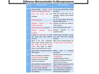
- 15. Difference Microcontroller Vs Microprocessor Sr.no . Microcontroller Microprocessor 1 Microcontroller having inbuilt RAM or ROM and inbuilt timer. Do not have inbuilt RAM or ROM and timer. 2 Input and output ports are available. Input and output ports are not available, requires extra device like 8155 3 Inbuilt serial port. Do not have inbuilt serial port, requires 8250 device. 4 Separate memory to store program and data. Program and data are stored in same memory. 5 Many functions pins on the IC. Less multifunction pins on IC. 6 Boolean operation directly possible. Boolean operation is not possible directly. 7 It takes few instructions to read and write data from external memory. It take many instruction to read and write data from external memory. 8 Most of the micro controllers have power saving modes like idle mode and power saving mode. This helps to reduce power consumption even further. Most of the microprocessors do not have power saving features 9 Used mainly in washing machine, MP3 players Mainly used in personal computers 10 Micro controllers are based on Harvard architecture where program memory and Data memory are separate Microprocessors are based on Von Neumann model/architecture where program and data are stored in same memory module 11 Since external components are low, total power consumption is less and can be used with devices running on stored power like batteries. Due to external components, the entire power consumption is high. Hence it is not suitable to used with devices running on stored power like batteries.
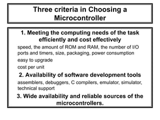
- 16. 1. Meeting the computing needs of the task efficiently and cost effectively speed, the amount of ROM and RAM, the number of I/O ports and timers, size, packaging, power consumption easy to upgrade cost per unit 2. Availability of software development tools assemblers, debuggers, C compilers, emulator, simulator, technical support 3. Wide availability and reliable sources of the microcontrollers. Three criteria in Choosing a Microcontroller
- 17. Block Diagram of Microcontroller CPU On-chip RAM On-chip ROM for program code 4 I/O Ports Timer 1 Serial PortOSC Interrupt Control External interrupts Timer 0 Timer/Counter Bus Control TxD RxDP0 P1 P2 P3 Address/Data Counter Inputs
- 18. Architecture of 8051 microcontroller P0 - - - - P7
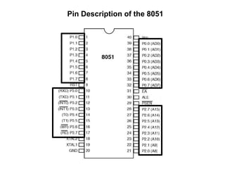
- 19. Pin Description of the 8051
- 20. Pins of 8051(1/4) • Vcc(pin 40): -Vcc provides supply voltage to the chip. -The voltage source is +5V. • GND(pin 20):ground • XTAL1 and XTAL2(pins 19,18)
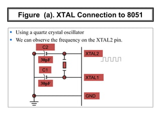
- 21. Figure (a). XTAL Connection to 8051 C2 30pF C1 30pF XTAL2 XTAL1 GND Using a quartz crystal oscillator We can observe the frequency on the XTAL2 pin.
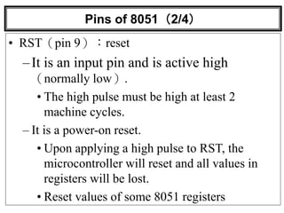
- 22. Pins of 8051(2/4) • RST(pin 9):reset –It is an input pin and is active high (normally low). • The high pulse must be high at least 2 machine cycles. – It is a power-on reset. • Upon applying a high pulse to RST, the microcontroller will reset and all values in registers will be lost. • Reset values of some 8051 registers
- 23. Pins of 8051(3/4) /EA(pin 31):external access. It can’t be left unconnected – There is no on-chip ROM in 8031 and 8032 . – The /EA pin is connected to GND to indicate the code is stored externally. – /PSEN & ALE are used for external ROM. – For 8051, /EA pin is connected to Vcc. – “/” means active low. /PSEN(pin 29):program store enable – Reads the external program memory. This is an output pin and is connected to the OE pin of the ROM.
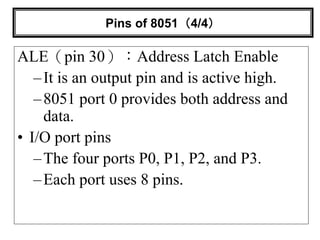
- 24. Pins of 8051(4/4) ALE(pin 30):Address Latch Enable –It is an output pin and is active high. –8051 port 0 provides both address and data. • I/O port pins –The four ports P0, P1, P2, and P3. –Each port uses 8 pins.
- 25. RAM memory space allocation in the 8051 7FH 30H 2FH 20H 1FH 17H 10H 0FH 07H 08H 18H 00H Register Bank 0 (Stack) Register Bank 1 Register Bank 2 Register Bank 3 Bit-Addressable RAM (16 bytes) Scratch pad RAM (80 bytes)
- 26. Stack in the 8051 • The register used to access the stack is called SP (stack pointer) register. • The stack pointer in the 8051 is only 8 bits wide, which means that it can take value 00 to FFH. When 8051 powered up, the SP register contains value 07. 7FH 30H 2FH 20H 1FH 17H 10H 0FH 07H 08H 18H 00H Register Bank 0 (Stack) Register Bank 1 Register Bank 2 Register Bank 3 Bit-Addressable RAM Scratch pad RAM
- 27. Registers A B R0 R1 R3 R4 R2 R5 R7 R6 DPH DPL PC DPTR PC Some 16-bit Registers Some 8-bit Registers of the 8051
- 28. 4 Register banks
- 29. RESET Value of Some 8051 Registers 0000DPTR 0007SP 0000PSW 0000B 0000ACC 0000PC Reset ValueRegister RAM are all zero.
- 30. Pins of I/O Port The 8051 has four I/O ports – Port 0 (pins 32-39):P0(P0.0~P0.7) – Port 1(pins 1-8) :P1(P1.0~P1.7) – Port 2(pins 21-28):P2(P2.0~P2.7) – Port 3(pins 10-17):P3(P3.0~P3.7) – Each port has 8 pins. • Named P0.X (X=0,1,...,7), P1.X, P2.X, P3.X • Ex:P0.0 is the bit 0(LSB)of P0 • Ex:P0.7 is the bit 7(MSB)of P0 • These 8 bits form a byte. Each port can be used as input or output (bi-direction).
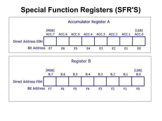
- 31. Special Function Registers (SFR'S) There are 21 Special function registers (SFR) in 8051 microcontroller and this includes Register A, Register B, Program Status Word (PSW), PCON etc. There are 21 unique locations for these 21 special function registers and each of these register is of 1 byte size. Some of these special function registers are bit addressable (which means you can access 8 individual bits inside a single byte), while some others are only byte addressable.
- 32. Special Function Registers (SFR'S)
- 33. Special Function Registers (SFR'S)
- 34. Special Function Registers (SFR'S) Stack Pointer Stack pointer is an 8 bit register, the direct address of SP is 81H and it is only byte addressable, which means you cant access individual bits of stack pointer. Usually after a system reset SP is initialized as 07H and data can be stored to stack from 08H onwards. This is usually a default case and programmer can alter values of SP to suit his needs.
- 35. Special Function Registers (SFR'S) Power Management Register (PCON)
- 36. Special Function Registers (SFR'S) Program Status Word (PSW)
- 37. Program Status Word (PSW) Continued....
- 38. SFR Addresses ( 1 of 2 )
- 39. SFR Addresses ( 2 of 2 )
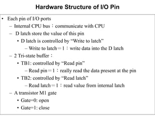
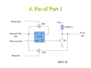
- 40. Hardware Structure of I/O Pin • Each pin of I/O ports – Internal CPU bus:communicate with CPU – D latch store the value of this pin • D latch is controlled by “Write to latch” – Write to latch=1:write data into the D latch – 2 Tri-state buffer: • TB1: controlled by “Read pin” – Read pin=1:really read the data present at the pin • TB2: controlled by “Read latch” – Read latch=1:read value from internal latch – A transistor M1 gate • Gate=0: open • Gate=1: close
- 41. A Pin of Port 1 8051 IC D Q Clk Q Vcc Load(L1) Read latch Read pin Write to latch Internal CPU bus M1 P1.X pinP1.X TB1 TB2
- 42. Writing “1” to Output Pin P1.X D Q Clk Q Vcc Load(L1) Read latch Read pin Write to latch Internal CPU bus M1 P1.X pinP1.X 2. output pin is Vcc1. write a 1 to the pin 1 0 output 1 TB1 TB2
- 43. Writing “0” to Output Pin P1.X D Q Clk Q Vcc Load(L1) Read latch Read pin Write to latch Internal CPU bus M1 P1.X pinP1.X 2. output pin is ground1. write a 0 to the pin 0 1 output 0 TB1 TB2
- 44. Reading “High” at Input Pin D Q Clk Q Vcc Load(L1) Read latch Read pin Write to latch Internal CPU bus M1 P1.X pin P1.X 8051 IC 2. MOV A,P1 external pin=High 1. write a 1 to the pin MOV P1,#0FFH 1 0 3. Read pin=1 Read latch=0 1 TB1 TB2
- 45. Reading “Low” at Input Pin D Q Clk Q Vcc Load(L1) Read latch Read pin Write to latch Internal CPU bus M1 P1.X pin P1.X 8051 IC 2. MOV A,P1 external pin=Low1. write a 1 to the pin MOV P1,#0FFH 1 0 3. Read pin=1 Read latch=0 0 TB1 TB2
- 46. Other Pins • P1, P2, and P3 have internal pull-up resisters. – P1, P2, and P3 are not open drain. • P0 has no internal pull-up resistors and does not connects to Vcc inside the 8051. – P0 is open drain(used in MOS) • However, for a programmer, it is the same to program P0, P1, P2 and P3. • All the ports upon RESET are configured as output.
- 47. A Pin of Port 0 8051 IC D Q Clk Q Read latch Read pin Write to latch Internal CPU bus M1 P0.X pinP0.X TB1 TB2 1. write a 1 to the pin 1 0 Output pin floating
- 48. Port 0 with Pull-Up Resistors P0.0 P0.1 P0.2 P0.3 P0.4 P0.5 P0.6 P0.7 Vcc 10 K Port0
- 49. Port 3 Alternate Functions
- 50. Addressing Modes Addressing modes specifies where the data (operand) is. They specify the source or destination of data (operand) in several different ways, depending upon the situation. Addressing modes are used to know where the operand located is.
- 51. There are 5 types of addressing modes: 1. Register (direct) addressing. 2. Direct addressing. 3. Register indirect addressing. 4. Immediate addressing. 5. Index addressing.
- 52. 1.Register (Direct) Addressing Mode In register addressing mode; the source and/or destination is a register. In this case; data is placed in any of the 8 registers(R0-R7); in instructions it is specified with letter Rn (where ‘n’ indicates 0 to 7). For example; 1.MOV A, Rn (This is general instruction). 2.ADD A, R5 (This instruction will add the contents of register R5 with the accumulator contents).
- 53. 2.Direct Addressing Mode In direct addressing mode; the address of memory location containing data to be read is specified in instruction. In this case; address of the data is given with the instruction itself. E.g.: MOV A, 25H (This instruction will read/move the data from internal RAM address 25H and store it in the accumulator. 25H (address) 1F To ACC. (A)
- 54. 3.Register Indirect Addressing Mode In register indirect addressing mode; the contents of the designated register are used as a pointer to memory. In this case; data is placed in memory, but address of memory location is not given directly with instruction e.g.: MOV A,@R0 This instruction moves the data from the register whose address is in the R0 register into the accumulator. R0 20H(address) 2F To ACC.(A)
- 55. 4.Immediate Addressing Mode In immediate addressing mode, the data is given with the instruction itself. In this case; the data to be stored in memory immediately follows the opcode. e.g.: MOV A, #25H (This instruction will move the data 25H to accumulator. ‘#’ means immediate 25H To ACC (A)
- 56. 5.Index Addressing Mode Offset (from accumulator) is added to the base index register( DPTR OR Program Counter) to form the effective address of the memory location. In this case; this mode is made for reading tables in the program memory. For example; MOVC A, @ A + DPTR ( This instruction moves the data from the memory to accumulator; whose address is computed by adding the contents of accumulator and DPTR)
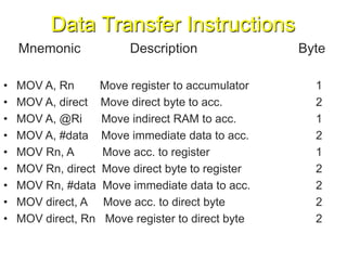
- 57. Data Transfer Instructions Mnemonic Description Byte • MOV A, Rn Move register to accumulator 1 • MOV A, direct Move direct byte to acc. 2 • MOV A, @Ri Move indirect RAM to acc. 1 • MOV A, #data Move immediate data to acc. 2 • MOV Rn, A Move acc. to register 1 • MOV Rn, direct Move direct byte to register 2 • MOV Rn, #data Move immediate data to acc. 2 • MOV direct, A Move acc. to direct byte 2 • MOV direct, Rn Move register to direct byte 2
- 58. Mnemonic Description Byte MOV direct, direct Move direct byte to direct 3 MOV direct, @ Ri Move direct RAM to direct byte 2 MOV direct, # data Move immediate data to direct byte 3 MOV @ Ri, A Move Acc. to indirect RAM 1 MOV @ Ri, direct Move direct byte to indirect RAM 2 MOV @ Ri, #data Move immediate data to indirect RAM 2 MOV DPTR, #data Move immediate data to DPTR 3 MOVC A @ A+DPTR Move code byte relative to DPTR to acc. 1 MOVC A@ A+PC Move code byte relative to PC to acc. 1
- 59. Mnemonic Description Byte MOVX A,@ Ri Move external RAM to acc. 8 bit 1 MOVX A, @ DPTR Move external RAM to acc 16 bit 1 MOVX @Ri, A Move acc. to external RAM 8 bit 1 MOVX @DPTR, A Move acc. to external RAM 16 bit 1 PUSH direct Push direct byte onto stack 2 POP direct Pop direct byte from stack 2 XCH A, Rn Exchange register with acc. 1 XCH A, direct Exchange direct byte with acc.2 XCH A, @Ri Exchange indirect RAM with acc. 1
- 60. Arithmetic Instructions Mnemonic Description Byte ADD A, Rn Add register to acc. 1 ADD A, direct Add direct byte to acc. 2 ADD A, @ Ri Add indirect RAM to acc. 1 ADD A, # data Add immediate data to acc. 2 ADDC A, Rn Add register to acc with carry 1 ADDC A , direct Add direct byte to acc with carry 2 ADDC A, @ Ri Add indirect RAM to acc with carry 1 ADDC A, # data Add immediate data to acc with carry 2 SUBB A, Rn Subtract register from acc with borrow 1
- 61. SUBB A, direct Subtract direct byte from acc with borrow 2 SUBB A, @ Ri Subtract Indirect RAM from acc with borrow 1 SUBB A, # data Subtract immediate data from acc with borrow 2 INC A Increment accumulator 1 INC Rn Increment register 1 INC direct Increment direct byte 2 INC @ Ri Increment indirect RAM 1 DEC A Decrement acc. 1 DEC Rn Decrement register 1 DEC direct Decrement direct byte 2 DEC @ Ri Decrement indirect RAM 1 INC DPTR Decrement data pointer 1 MUL AB Multiply A and B 1 DIV AB Divide A by B 1 Mnemonic Description Byte
- 62. Logical Instructions Mnemonic Description Byte ANL A, Rn AND register to acc 1 ANL A, direct AND direct byte to acc 2 ANL A,@ Ri AND indirect RAM to acc 1 ANL A, # data AND immediate data to acc 2 ANL direct, A AND acc to direct byte 2 ANL direct,# data AND immediate data to direct byte 3 ORL A, Rn OR register to acc 1 ORL A, direct OR direct byte to acc 2 ORL A, @ Ri OR indirect RAM to acc 1 ORL A, # data OR immediate data to acc 2 ORL direct, A OR acc to direct byte 2 ORL direct, #data OR immediate data to direct byte 3
- 63. Mnemonic Description Byte XRL A, Rn EX-OR register to acc 1 XORL A, direct EX-OR direct byte to acc 2 XORL A,@ Ri EX-OR indirect RAM to acc 1 XORL A, # data EX-OR immediate data to acc 2 XORL direct, A EX-OR acc to direct byte 2 XORL direct, # data EX-OR immediate data to direct byte 3 CLR A Clear accumulator 1 CPL A Complement accumulator 1 SWAP A Swap nibble within acc 1 RL A Rotate acc left 1 RLC A Rotate acc left through carry 1 RR A Rotate acc right 1 RRC A Rotate acc right through carry 1
- 64. Logical Instructions On Bits Mnemonic Description Byte CLR C Clear carry 1 CLR bit Clear direct bit 2 SETB C Set carry 1 SETB bit Set direct bit 2 CPL C Complement carry 1 CPL bit Complement direct bit 2 ANL C, bit AND direct bit to carry 2 ANL C,/bit AND complement of direct bit to carry 2 ORL C, bit OR direct bit to carry 2 ORL C,/bit OR complement direct to bit to carry 2 MOV C, bit Move direct bit to carry 2 MOV bit, C Move carry to direct bit 2
- 67. MOV instruction MOV destination, source ; copy source to destination MOV instruction copies data from one location to another. This instruction tells the CPU to copy the source operand to the destination operand. “MOV A, R0” copies the contents of register R0 to acc. After this instruction is executed, register A will have the same value as register R0. MOV A, #55H ; Load value 55H into register A (A=55H) MOV R0, A ; copy contents of A into R0 (A=R0=55H)
- 68. ADD instruction • ADD A, source ; ADD the source operand to acc MOV A, #20H ; load 20H into A MOV R0, #30H ; load 30H into R0 ADD A, R0 ; add R0 to acc ; (A=A+R0) OR MOV A, #20H ; Load one operand into A ADD A, #30H ; add the second operand 30H to A
- 69. Some important terms Machine language: “A program consists of 0s and 1s is called as machine language” Assembly language programs must be translated into machine code by a program called an “assembler” Assembly language is referred to as a “Low- level language”, it deals directly with the internal structure of CPU. To program in Assembly language, the programmer must know all the registers of the CPU and size of each, also other details.
- 70. • C, C++, Java and numerous other languages are called “High-level languages” because the programmer does not have to be concerned with internal details of CPU. • “Assembler” is used to translate an Assembly language program into machine code(sometimes also called object code or opcode or operation code) • “High level languages are translated into machine code by a program called a compiler”.
- 71. Steps to create a program Myfile.lst EDITOR PROGRAM ASSEMBLER PROGRAM LINKER PROGRAM OH PROGRAM Myfile.asm Other .obj fileMyfile.obj Myfile.abs Myfile.hex
- 72. Unconditional Jump Instructions All conditional jumps are short jumps – Target address within -128 to +127 of PC LJMP (long jump): 3-byte instruction – 2-byte target address: 0000 to FFFFH – Original 8051 has only 4KB on-chip ROM SJMP (short jump): 2-byte instruction – 1-byte relative address: -128 to +127
- 73. Call Instructions LCALL (long call): 3-byte instruction – 2-byte address – Target address within 64K-byte range ACALL (absolute call): 2-byte instruction – 11-bit address – Target address within 2K-byte range
- 74. Basics of Serial Communication • Computers transfer data in two ways: – Parallel: Often 8 or more lines (wire conductors) are used to transfer data to a device that is only a few feet away. – Serial: To transfer to a device located many meters away, the serial method is used. The data is sent one bit at a time.
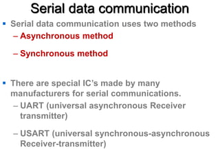
- 76. Serial data communication Serial data communication uses two methods – Asynchronous method – Synchronous method There are special IC’s made by many manufacturers for serial communications. – UART (universal asynchronous Receiver transmitter) – USART (universal synchronous-asynchronous Receiver-transmitter)
- 77. Asynchronous – Start & Stop Bit Asynchronous serial data communication is widely used for character-oriented transmissions – Each character is placed in between start and stop bits, this is called framing. – Block-oriented data transfers use the synchronous method. The start bit is always one bit, but the stop bit can be one or two bits The start bit is always a 0 (low) and the stop bit(s) is 1 (high)
- 78. Asynchronous – Start & Stop Bit 41H
- 79. Data Transfer Rate The rate of data transfer in serial data communication is stated in bps (bits per second). Another widely used terminology for bps is baud rate. – It is modem terminology and is defined as the number of signal changes per second – In modems, there are occasions when a single change of signal transfers several bits of data As far as the conductor wire is concerned, the baud rate and bps are the same.
- 80. Machine cycle calculation 1 machine cycle = 12 clock cycles
- 81. RS232 connector
- 83. MAX232 (Serial interface with PC)
- 84. Baud Rate • No. of signal changes per second is called as Baud Rate • The rate of data transfer in serial data communication is stated in BPS(Bits Per Second) • As far as conductor wire is concerned, the baud rate and bps are the same • The 8051’s serial communication UART circuitry divides the machine cycle frequency of 921.6 KHz by 32 gives 28800Hz.
- 85. PC Baud Rates
- 86. SCON (Serial control) register
- 87. SBUF Register Serial Buffer is an 8 bit register. For a byte (8 bit) of data to be transferred via the TXD line, it must be placed in the serial buffer register. Similarly SBUF register holds the byte of data when it is received by the 8051’s RXD line.
- 88. Operating Modes SM0 SM1 Trans. format Baud Rate 0 0 Serial Mode 0, , 8 bits 1/12 * 0 1 Serial Mode 1,8 bit data, variable 1 stop bit, 1 start bit(10bits) 1 0 Serial Mode 2 1/32 or 1/64 11 bits(1 start, 1 stop, 8 bit data, 9th bit programmble) 1 1 Serial Mode 3 variable 11 bits(1 start, 1 stop, 8 bit data, 9th bit programmble)
- 89. Steps to write a program 1) Load TMOD register with the value 20H, indicating the use of timer 1,mode 2 (8 bit auto - reload) to set the baud rate. 2) Then TH1 is loaded with one of the values shown in Table 10-4 3) SCON is loaded with value 50 H, indicating serial mode 1. 4) TR1 is set to 1 to start timer 1 5) Charact. To be transferred is written into SBUF 6) TI is flag is monitored with the use of the information “JNB TI ,xx” 7) TI is cleared by “CLR TI” instruction 8) Keep sending “A”
- 90. Programming the 8051 to transfer data serially
- 91. Baud rates for SMOD=0 Machine cycle freq. = 11.0592 MHz / 12 = 921.6 kHz and 921.6 kHz / 32 = 28,800 Hz since SMOD = 0
- 92. Doubling the baud rate in the 8051 By Doubling the crystal frequency By making SMOD= 1 of PCON register
- 94. Timer/Counter 8051 has two timers/Counters. They can be used either as Timer to generate time delay. Or as Counter to Count Events outside microcontroller. Timer 0 (T0) : 16 bit wide TH0(8) TL0(8) Timer 1 (T1): 16 bit wide TH1(8) TL1(8)
- 98. Mode 1 programming 1.Loaded value into TL and TH 2.”SETB TR0” for timer 0 ;”SETB TR1” for timer 1 3.If TF (timer flag) = high “CLR TR0” or “CLR TR1” 4.Reloaded TH and TL value, TF reset to 0
- 100. TCON Register
- 101. References Sr. No. Title of Book Authors Publication House 1 “8051Microcontroller” Scott Mackenzie Pearson Education. 2 “8051 microcontroller” Subrata Ghoshal, Pearsons Publishers. 3 “Microprocessor and Microcontroller” Theagrajan BS Publication Text books : Sr. No. Title of Book Authors Publication House 1 “The 8051 Microcontroller and Embedded Systems” Muhammad Ali Mazidi, J.G. Mazidi Pearsons Publishers 2 “8051 Microcontroller, Hardware, software and applications” V Udayashankara and M S MallikarjunaSwamy TATA McGraw Hill 3 “Microcontroller 8051” Ajay Deshmukh TATA McGraw Hill. 4 “The 8051 Microcontrollers- Architecture, Programming and Applications” K. J. Ayala Peram International Publications Reference books: