
 Data Structure
 Networking
 RDBMS
RDBMS Operating System
 Java
Java MS Excel
 iOS
iOS HTML
HTML CSS
CSS Android
 Python
 C Programming
 C++
C++ C#
C# MongoDB
 MySQL
MySQL Javascript
 PHP
PHP
- Selected Reading
- UPSC IAS Exams Notes
- Developer's Best Practices
- Questions and Answers
- Effective Resume Writing
- HR Interview Questions
- Computer Glossary
- Who is Who
Interfacing 8251 USART with 8085 Microprocessor
The 8251 chip is Universal Synchronous Asynchronous Receiver Transmitter (USART). It acts as a mediator between the microprocessor and peripheral devices. It converts serial data to parallel form and vice versa. This chip is 28 pin DIP.
The pin description of 8251A chip

| Pin |
Description |
|---|---|
|
D0 - D7 |
parallel data |
|
C/D |
Control register or Data buffer select |
|
RD |
Read Control |
|
WR |
Write control |
|
CS |
Chip Select |
|
CLK |
clock pulse |
|
RESET |
Reset |
|
TxC |
Transmitter Clock |
|
TxD |
transmitted data |
|
RxC |
Receiver Clock |
|
RxD |
Receiver Data |
|
RxRDY |
Receiver Ready |
|
TxRDY |
Transmitter Ready |
|
DSR |
Data Set Ready |
|
DTR |
Data Terminal Ready |
|
SYNDET/ |
Synchronous Detect/ |
|
BRKDET |
DetectBreak |
|
RTS |
Request to send Data |
|
CTS |
Clear to send Data |
|
TxEMPTY |
Transmitter Empty |
|
Vcc |
Vcc (5V) |
|
GND |
Ground(0V) |
Now let us see the functional block diagram of the 8251 chip.
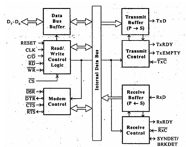
There are five different sections in this diagram. These sections are as follows −
Read/ Write control logic
Transmitter
Receiver
Data Bus Buffer
Modem Control.
Interfacing 8251 with8085
Now let us see how 8251 can be interfaced with 8085. In the diagram, we can see that eight data lines D7-0 are connected to the data bus of the microprocessor. And also the RD and WR of the 8251 are also connected with the RD and RD of 8051. The 8251 is getting the clock from the CLK OUT pin of 8085. And the RESET is also connected to the RESET OUT pin of the microprocessor.

The C/D pin is used to select either control register or data register. This pin is connected to the A0 pin of 8085. The CS pin of 8251 is attached to the output of an address decoder circuit. The address decoder uses A7 to A1 lines of the microprocessor. In this diagram the CS will be enabled when A7 and A4 is at logic 1, and all other lines are at logic 0.
From the following table, we can see how to read or write data word, read the status word and write control word.
| A0 |
RD |
WR |
Task |
Port Address |
|---|---|---|---|---|
| 0 |
0 |
1 |
Read Data Word |
90H |
| 0 |
1 |
0 |
Write Data Word |
90H |
| 1 |
0 |
1 |
Read Status Word |
91H |
| 1 |
1 |
0 |
Write Control Word |
91H |

20K+ Views
